Optimizing Designs for Alteras MAX 7000 Devices Copyright


![Executing the Jam Player n jbi or jam [-h] [-v] [-d <var=val>] [-p <port>] Executing the Jam Player n jbi or jam [-h] [-v] [-d <var=val>] [-p <port>]](https://slidetodoc.com/presentation_image/34aa1f691e49440f467bcaf796d6e3e1/image-145.jpg)
![Executing the Jam Player n jbi or jam [-h] [-v] [-d <var=val>] [-p <port>] Executing the Jam Player n jbi or jam [-h] [-v] [-d <var=val>] [-p <port>]](https://slidetodoc.com/presentation_image/34aa1f691e49440f467bcaf796d6e3e1/image-146.jpg)

- Slides: 185

Optimizing Designs for Altera’s MAX 7000 Devices Copyright © 1998 Altera Corporation

Course Outline n SECTION 1: MAX 7000 Family Overview n SECTION 2: MAX 7000 Device Architecture – Laboratory Exercise #1 n SECTION 3: Design Methodology and Guidelines for MAX 7000 Devices – Design Entry Techniques – Resolving Fitting Issues • Laboratory Exercise #2 – Resolving Performance Issues • Laboratory Exercise #3 n SECTION 4: Programming MAX 7000 Devices – Laboratory Exercise #4 Copyright © 1998 Altera Corporation

SECTION 1 MAX 7000 Family Overview Copyright © 1998 Altera Corporation

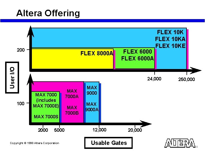
Altera Offering 200 User I/O FLEX 8000 A FLEX 6000 A FLEX 10 KA FLEX 10 KE 24, 000 100 MAX 7000 (includes MAX 7000 E) MAX 7000 S 2000 5000 Copyright © 1998 Altera Corporation MAX 7000 A MAX 7000 B MAX 9000 A 12, 000 Usable Gates 20, 000 250, 000

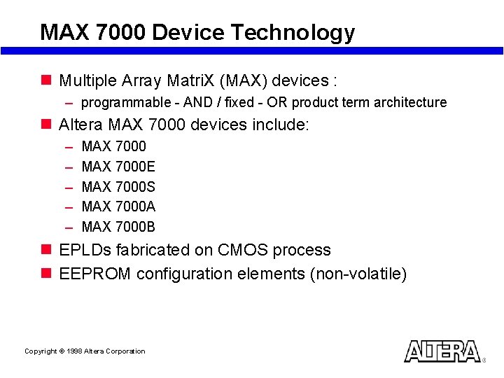
MAX 7000 Device Technology n Multiple Array Matri. X (MAX) devices : – programmable - AND / fixed - OR product term architecture n Altera MAX 7000 devices include: – – – MAX 7000 E MAX 7000 S MAX 7000 A MAX 7000 B n EPLDs fabricated on CMOS process n EEPROM configuration elements (non-volatile) Copyright © 1998 Altera Corporation

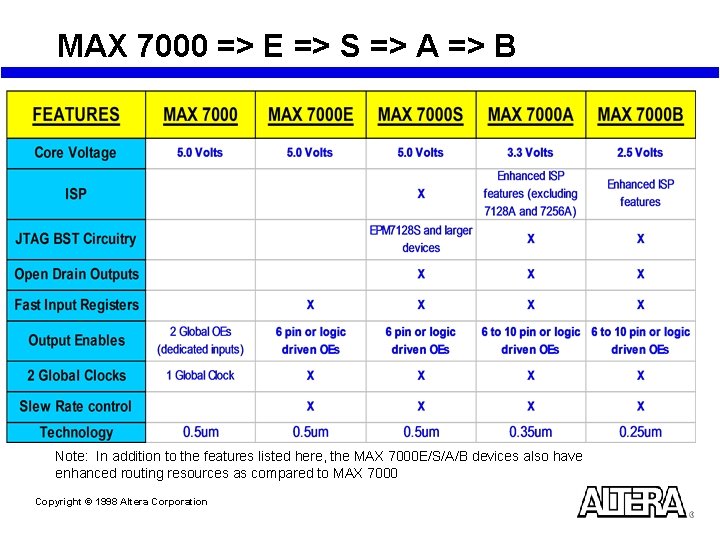
MAX 7000 => E => S => A => B Note: In addition to the features listed here, the MAX 7000 E/S/A/B devices also have enhanced routing resources as compared to MAX 7000 Copyright © 1998 Altera Corporation

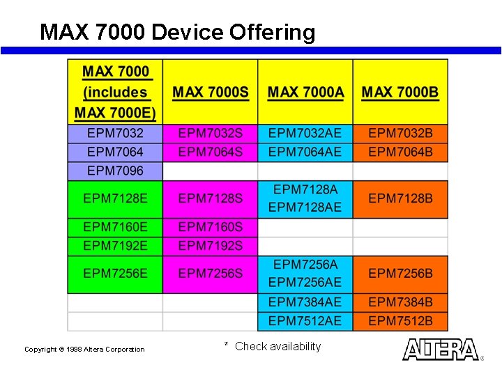
MAX 7000 Device Offering Copyright © 1998 Altera Corporation * Check availability

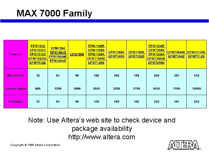
MAX 7000 Family Note: Use Altera’s web site to check device and package availability http: //www. altera. com Copyright © 1998 Altera Corporation

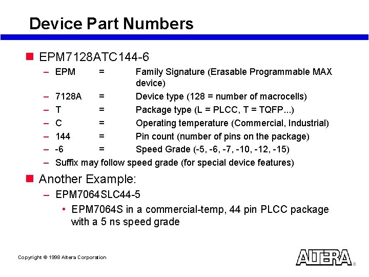
Device Part Numbers n EPM 7128 ATC 144 -6 – EPM – – – = Family Signature (Erasable Programmable MAX device) 7128 A = Device type (128 = number of macrocells) T = Package type (L = PLCC, T = TQFP. . . ) C = Operating temperature (Commercial, Industrial) 144 = Pin count (number of pins on the package) -6 = Speed Grade (-5, -6, -7, -10, -12, -15) Suffix may follow speed grade (for special device features) n Another Example: – EPM 7064 SLC 44 -5 • EPM 7064 S in a commercial-temp, 44 pin PLCC package with a 5 ns speed grade Copyright © 1998 Altera Corporation

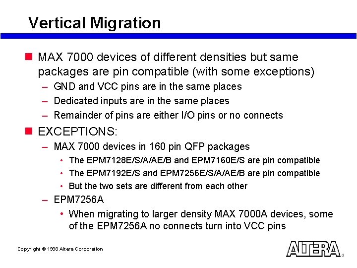
Vertical Migration n MAX 7000 devices of different densities but same packages are pin compatible (with some exceptions) – GND and VCC pins are in the same places – Dedicated inputs are in the same places – Remainder of pins are either I/O pins or no connects n EXCEPTIONS: – MAX 7000 devices in 160 pin QFP packages • The EPM 7128 E/S/A/AE/B and EPM 7160 E/S are pin compatible • The EPM 7192 E/S and EPM 7256 E/S/A/AE/B are pin compatible • But the two sets are different from each other – EPM 7256 A • When migrating to larger density MAX 7000 A devices, some of the EPM 7256 A no connects turn into VCC pins Copyright © 1998 Altera Corporation

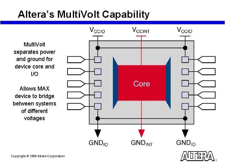
Altera’s Multi. Volt Capability Multi. Volt separates power and ground for device core and I/O Allows MAX device to bridge between systems of different voltages Copyright © 1998 Altera Corporation

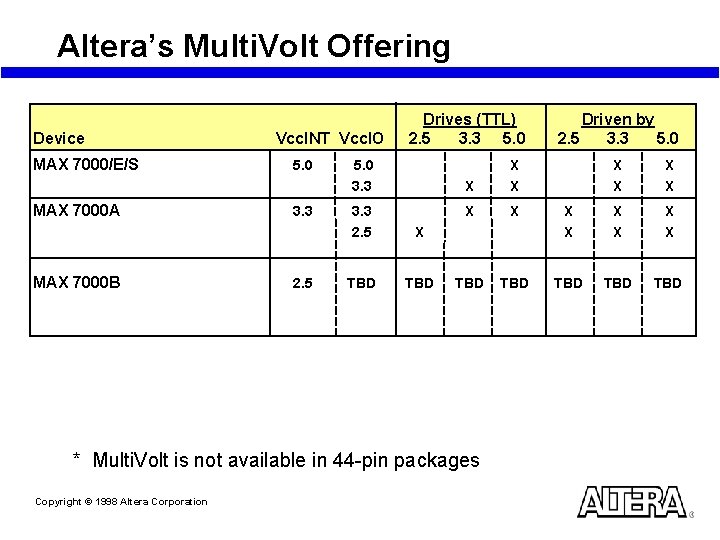
Altera’s Multi. Volt Offering Device MAX 7000/E/S MAX 7000 A MAX 7000 B Vcc. INT Vcc. IO 5. 0 3. 3 2. 5 Drives (TTL) 2. 5 3. 3 5. 0 3. 3 2. 5 X TBD X X X TBD TBD TBD * Multi. Volt is not available in 44 -pin packages Copyright © 1998 Altera Corporation Driven by 2. 5 3. 3 5. 0 X X

Turbo Bit n MAX 7000 devices offer low-power OR high speed operation n Total power dissipation can be reduced by 50% or more n This is controllable for the entire device OR on a macrocell by macrocell basis – A section of the design can operate in high performance (Turbo Bit = ON) and other sections may operate in low power (Turbo Bit = OFF) – MAX 7000 devices: macrocells running at low power (Turbo Bit = OFF) incur a delay t. LPA (8 ns for -5 speed grade) for the t. LAD , t. LAC , t. IC, t. ACL t. EN, t. SEXP parameters Copyright © 1998 Altera Corporation

SECTION 2 MAX 7000 Device Architecture Copyright © 1998 Altera Corporation

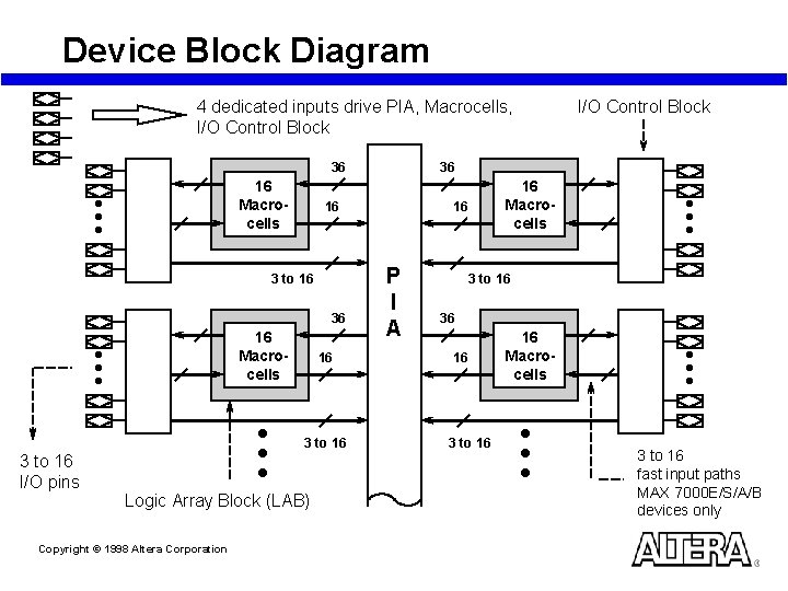
Altera MAX 7000 Device Terminology n Macrocell – The basic building block of a product term based device – Equivalent to a logic cell (term used to describe the basic building block of any Altera device) n Logic Array Block (LAB) – A group of logic cells – Each LAB in a MAX device contains 16 macrocells n Programmable Interconnect Array (PIA) – Continuous interconnect structure of a MAX 7000 device Copyright © 1998 Altera Corporation

Device Block Diagram 4 dedicated inputs drive PIA, Macrocells, I/O Control Block 36 36 16 Macrocells 16 3 to 16 I/O pins Logic Array Block (LAB) Copyright © 1998 Altera Corporation 16 Macrocells 16 16 3 to 16 I/O Control Block P I A 3 to 16 36 16 3 to 16 16 Macrocells 3 to 16 fast input paths MAX 7000 E/S/A/B devices only

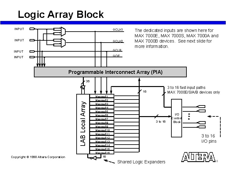
Logic Array Block INPUT GCLK 1 INPUT GCLK 2 INPUT GCLR INPUT GOE The dedicated inputs are shown here for MAX 7000 E, MAX 7000 S, MAX 7000 A and MAX 7000 B devices. See next slide for more information. Programmable Interconnect Array (PIA) 36 3 to 16 fast input paths MAX 7000 E/S/A/B devices only LAB Local Array 16 Copyright © 1998 Altera Corporation Macrocell 1 Macrocell 2 Macrocell 3 Macrocell 4 Macrocell 5 Macrocell 6 Macrocell 7 Macrocell 8 Macrocell 9 Macrocell 10 Macrocell 11 Macrocell 12 Macrocell 13 Macrocell 14 Macrocell 15 Macrocell 16 3 to 16 I/O Control Block 3 to 16 I/O pins 16 Shared Logic Expanders

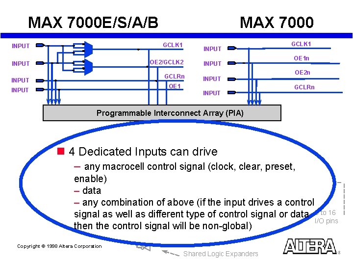
MAX 7000 E/S/A/B MAX 7000 INPUT GCLK 1 INPUT OE 2/GCLK 2 INPUT GCLRn INPUT OE 1 INPUT GCLK 1 OE 1 n OE 2 n GCLRn Programmable Interconnect Array (PIA) LAB Local Array n 4 Dedicated Inputs can drive – any macrocell control signal (clock, clear, preset, enable) – data – any combination of above (if the input drives a control signal as well as different type of control signal or data 6 to 16 I/O pins then the control signal will be non-global) Copyright © 1998 Altera Corporation Shared Logic Expanders

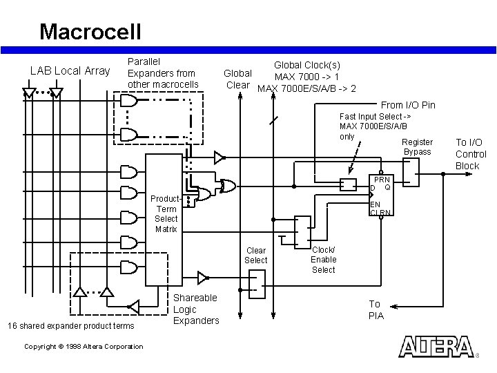
Macrocell LAB Local Array Parallel Expanders from other macrocells Global Clock(s) Global MAX 7000 -> 1 Clear MAX 7000 E/S/A/B -> 2 From I/O Pin Fast Input Select -> MAX 7000 E/S/A/B only Register Bypass PRN D Q Product. Term Select Matrix EN CLRN Clear Select 16 shared expander product terms Copyright © 1998 Altera Corporation Shareable Logic Expanders Clock/ Enable Select To PIA To I/O Control Block

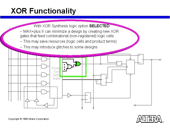
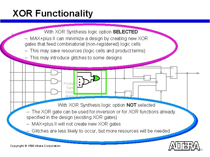
XOR Functionality With XOR Synthesis logic option SELECTED – MAX+plus II can minimize a design by creating new XOR gates that feed combinatorial (non-registered) logic cells – This may save resources (logic cells and product terms) – This may introduce glitches to some designs Product. Term Select Matrix Copyright © 1998 Altera Corporation

XOR Functionality With XOR Synthesis logic option SELECTED – MAX+plus II can minimize a design by creating new XOR gates that feed combinatorial (non-registered) logic cells – This may save resources (logic cells and product terms) – This may introduce glitches to some designs Product. Term Select Matrix With XOR Synthesis logic option NOT selected – The XOR gate can be used for inversion or for XOR functions already specified in the design (existing XOR gates) – MAX+plus II will not create new XOR gates – Glitches are less likely to occur, but more resources will be needed Copyright © 1998 Altera Corporation

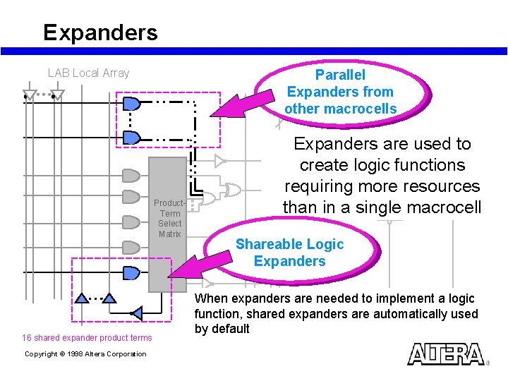
Expanders LAB Local Array Parallel Expanders from other macrocells Product. Term Select Matrix 16 shared expander product terms Copyright © 1998 Altera Corporation Expanders are used to create logic functions requiring more resources than in a single macrocell Shareable Logic Expanders When expanders are needed to implement a logic function, shared expanders are automatically used by default

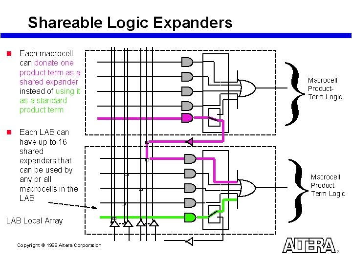
Shareable Logic Expanders n Each macrocell can donate one product term as a shared expander instead of using it as a standard product term n Each LAB can have up to 16 shared expanders that can be used by any or all macrocells in the LAB Local Array Copyright © 1998 Altera Corporation } } Macrocell Product. Term Logic ù ù ù Macrocell Product. Term Logic

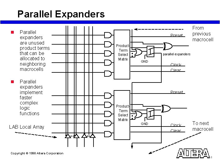
Parallel Expanders n n Parallel expanders are unused product terms that can be allocated to neighboring macrocells Parallel expanders implement faster complex logic functions LAB Local Array Copyright © 1998 Altera Corporation Preset Product. Term Select Matrix From previous macrocell parallel expanders GND Clock Clear Preset Product. Term Select Matrix GND Clock Clear To next macrocell

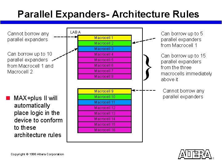
Parallel Expanders- Architecture Rules Cannot borrow any parallel expanders Can borrow up to 10 parallel expanders from Macrocell 1 and Macrocell 2 n MAX+plus II will automatically place logic in the device to conform to these architecture rules Copyright © 1998 Altera Corporation LAB A Can borrow up to 5 parallel expanders from Macrocell 1 Macrocell 2 Macrocell 3 Macrocell 4 Macrocell 5 Macrocell 6 Macrocell 7 Macrocell 8 Macrocell 9 Macrocell 10 Macrocell 11 Macrocell 12 Macrocell 13 Macrocell 14 Macrocell 15 Macrocell 16 } Can borrow up to 15 parallel expanders from the three macrocells immediately above it Cannot borrow any parallel expanders

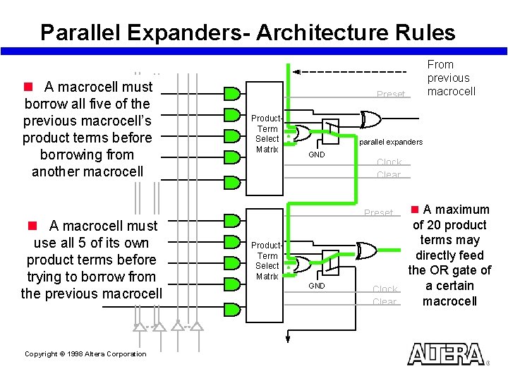
Parallel Expanders- Architecture Rules n A macrocell must borrow all five of the previous macrocell’s product terms before borrowing from another macrocell n A macrocell must use all 5 of its own product terms before trying to borrow from the previous macrocell Copyright © 1998 Altera Corporation From previous macrocell Preset Product. Term Select Matrix parallel expanders GND Clock Clear Preset Product. Term Select Matrix GND Clock Clear n A maximum of 20 product terms may directly feed the OR gate of a certain macrocell

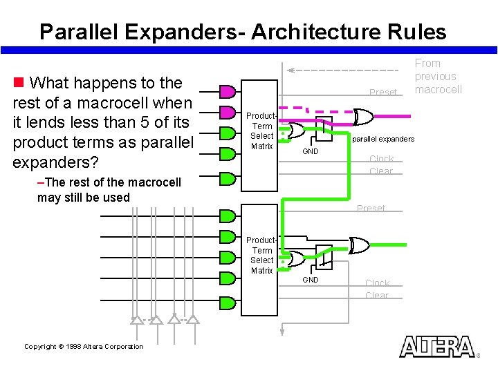
Parallel Expanders- Architecture Rules n What happens to the rest of a macrocell when it lends less than 5 of its product terms as parallel expanders? Preset Product. Term Select Matrix parallel expanders GND –The rest of the macrocell may still be used Clock Clear Preset Product. Term Select Matrix GND Copyright © 1998 Altera Corporation Clock Clear From previous macrocell

Parallel Expanders vs. Shareable Expanders Copyright © 1998 Altera Corporation

Logic Option Assignments n Logic options are “switches” that can be set in n n MAX+plus II that control the way MAX+plus II will implement your design in the MAX device A single logic option controls a single feature of the MAX device For example, enabling the Turbo Bit is controlled through a logic option The set of available logic options varies from device family to device family There are many features in MAX devices that are controllable; use logic options to get the most control over the MAX design Copyright © 1998 Altera Corporation

Logic Option Assignments - Examples n Parallel Expanders: Controls the use of parallel expanders to n n n implement the design Turbo Bit: Controls the use of the turbo bit either on a device-wide or macrocell-by-macrocell basis XOR Synthesis: Allows MAX+plus II to create new XOR gates from a given design to map to the XOR gate in the macrocell Fast I/O: Applied to input pins to enable the fast input path from an input pin directly to a macrocell register Slow Slew Rate: Applied to output pins in MAX 7000 E/S/A/B devices to slow down the output transitions Power-up High: Applied to an individual register in a MAX 7000 AE or MAX 7000 B device, that will cause the register to power up high (1) Global Signal: Applied to input pins to implement them on a dedicated input and make use of the global signal Copyright © 1998 Altera Corporation

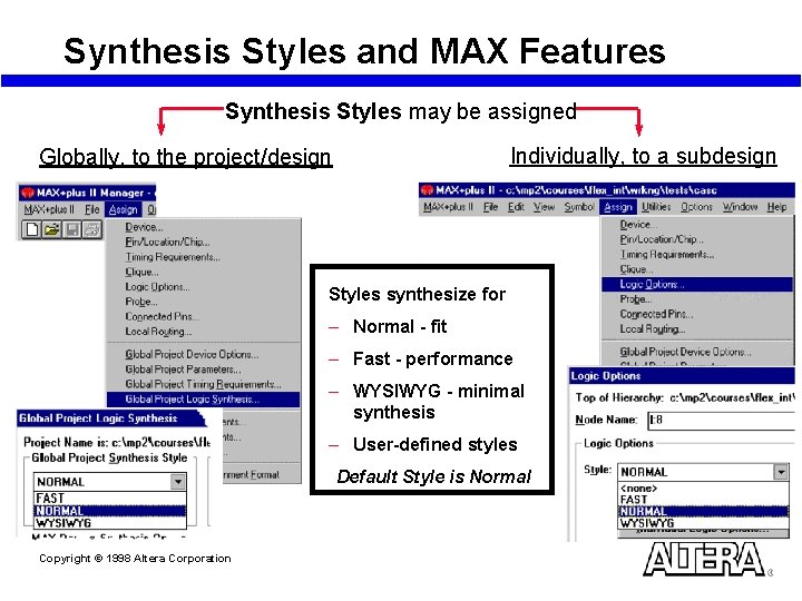
Synthesis Styles and MAX Features Synthesis Styles may be assigned Individually, to a subdesign Globally, to the project/design Styles synthesize for – Normal - fit – Fast - performance – WYSIWYG - minimal synthesis – User-defined styles Default Style is Normal Copyright © 1998 Altera Corporation

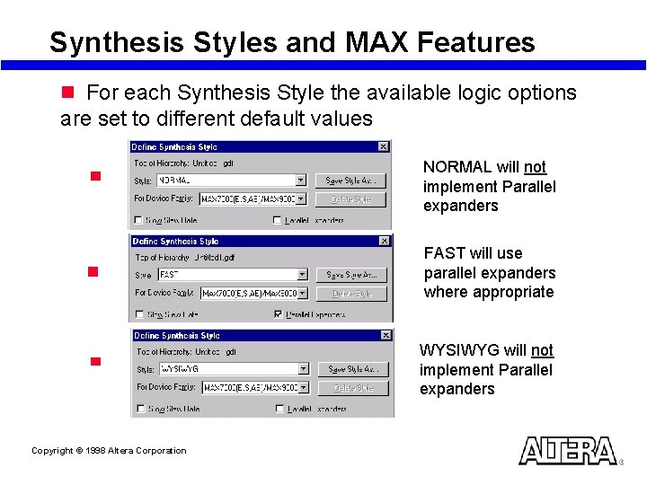
Synthesis Styles and MAX Features n For each Synthesis Style the available logic options are set to different default values NORMAL will not implement Parallel expanders FAST will use parallel expanders where appropriate WYSIWYG will not implement Parallel expanders Copyright © 1998 Altera Corporation

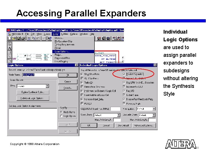
Accessing Parallel Expanders Individual Logic Options are used to assign parallel expanders to subdesigns without altering the Synthesis Style Copyright © 1998 Altera Corporation

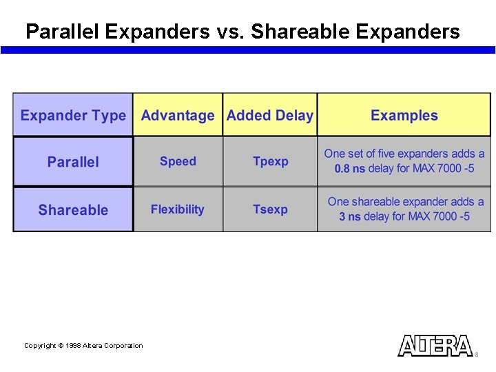
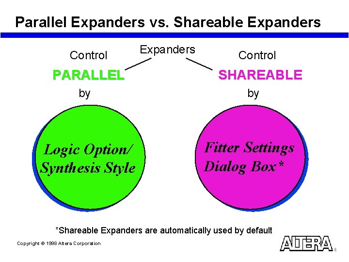
Parallel Expanders vs. Shareable Expanders Control PARALLEL by Logic Option/ Synthesis Style Expanders Control SHAREABLE by Fitter Settings Dialog Box* *Shareable Expanders are automatically used by default Copyright © 1998 Altera Corporation

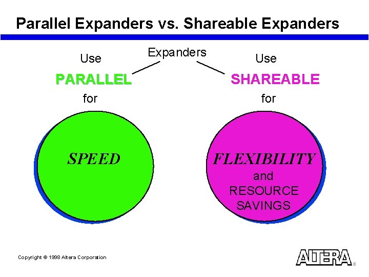
Parallel Expanders vs. Shareable Expanders Use PARALLEL for SPEED Expanders Use SHAREABLE for FLEXIBILITY and RESOURCE SAVINGS Copyright © 1998 Altera Corporation

Laboratory Exercise 1 Go to Laboratory Exercise Manual and Complete Exercise 1 Copyright © 1998 Altera Corporation

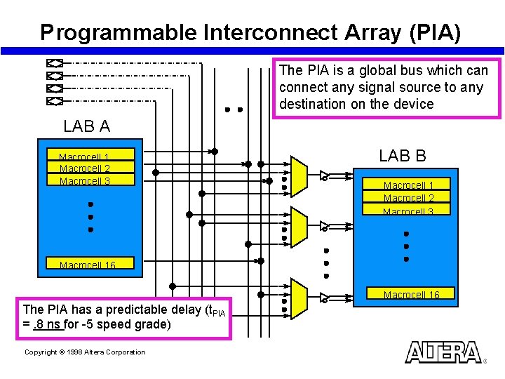
Programmable Interconnect Array (PIA) The PIA is a global bus which can connect any signal source to any destination on the device LAB A Macrocell 1 Macrocell 2 Macrocell 3 LAB B Macrocell 1 Macrocell 2 Macrocell 3 Macrocell 16 The PIA has a predictable delay (t. PIA =. 8 ns for -5 speed grade) Copyright © 1998 Altera Corporation

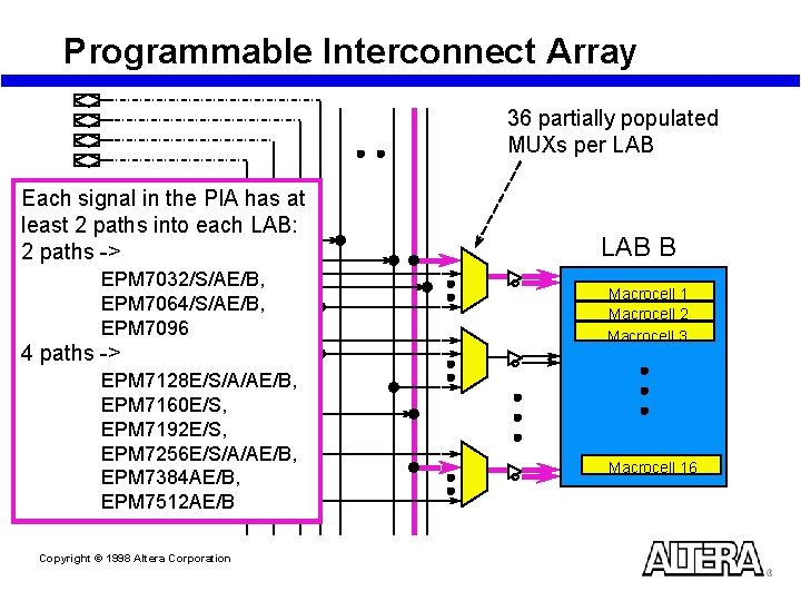
Programmable Interconnect Array 36 partially populated MUXs per LAB Each signal in the PIA has at least 2 paths into each LAB: 2 paths -> EPM 7032/S/AE/B, EPM 7064/S/AE/B, EPM 7096 4 paths -> EPM 7128 E/S/A/AE/B, EPM 7160 E/S, EPM 7192 E/S, EPM 7256 E/S/A/AE/B, EPM 7384 AE/B, EPM 7512 AE/B Copyright © 1998 Altera Corporation LAB B Macrocell 1 Macrocell 2 Macrocell 3 Macrocell 16

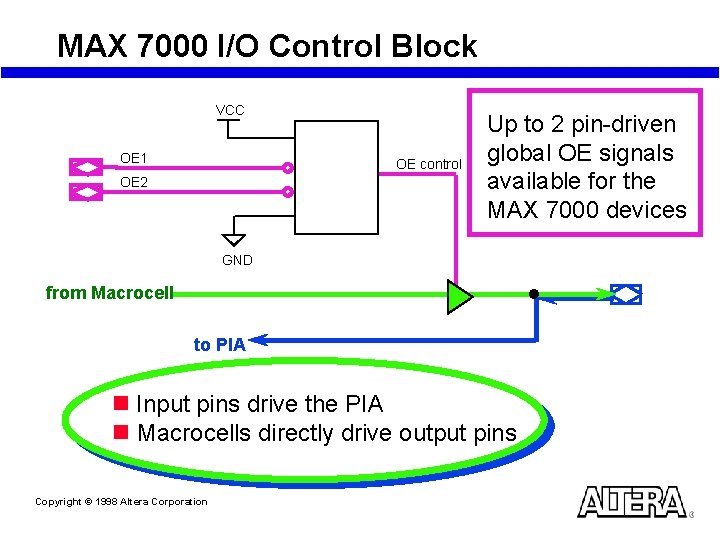
MAX 7000 I/O Control Block VCC OE 1 OE control OE 2 Up to 2 pin-driven global OE signals available for the MAX 7000 devices GND from Macrocell to PIA n Input pins drive the PIA n Macrocells directly drive output pins Copyright © 1998 Altera Corporation

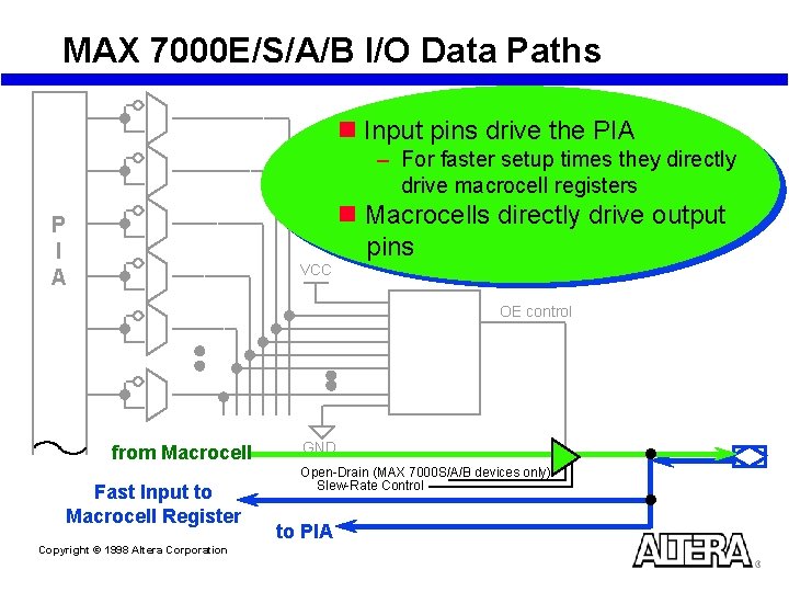
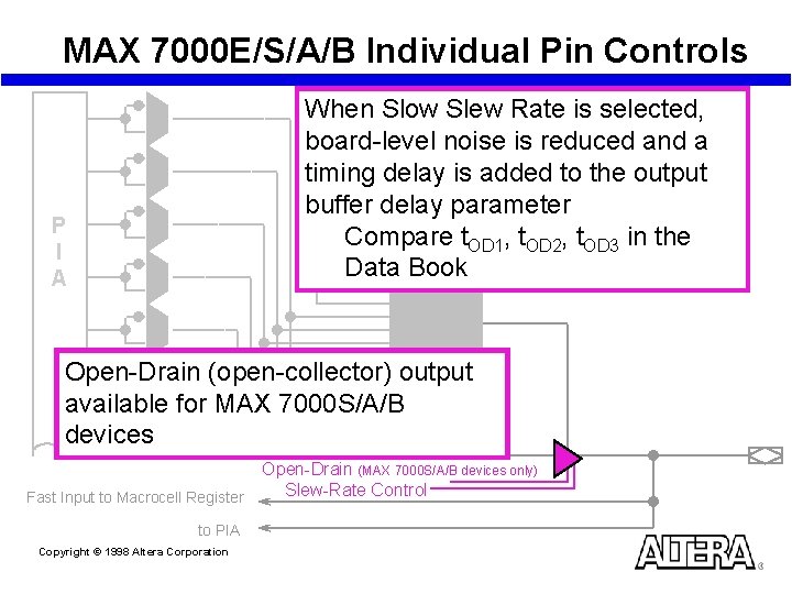
MAX 7000 E/S/A/B I/O Data Paths n Input pins drive the PIA – For faster setup times they directly drive macrocell registers n Macrocells directly drive output pins P I A VCC OE control from Macrocell Fast Input to Macrocell Register Copyright © 1998 Altera Corporation GND Open-Drain (MAX 7000 S/A/B devices only) Slew-Rate Control to PIA

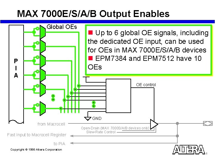
MAX 7000 E/S/A/B Output Enables Global OEs P I A n Up to 6 global OE signals, including the dedicated OE input, can be used for OEs in MAX 7000 E/S/A/B devices n EPM 7384 and EPM 7512 have 10 OEs OE control GND from Macrocell Fast Input to Macrocell Register to PIA Copyright © 1998 Altera Corporation Open-Drain (MAX 7000 S/A/B devices only) Slew-Rate Control

MAX 7000 E/S/A/B Individual Pin Controls When Slow Slew Rate is selected, board-level noise is reduced and a timing delay is added to the output buffer delay parameter Compare t. OD 1, t. OD 2, t. OD 3 in the Data Book P I A Open-Drain (open-collector) output available for MAX 7000 S/A/B devices Fast Input to Macrocell Register to PIA Copyright © 1998 Altera Corporation Open-Drain (MAX 7000 S/A/B devices only) Slew-Rate Control

SECTION 3 Design Methodology and Guidelines for MAX 7000 Devices Copyright © 1998 Altera Corporation

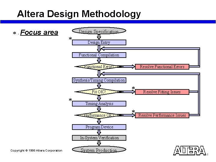
Altera Design Methodology * - Focus area Design Specification * Design Entry Functional Compilation Resolve Functional Errors Functional Error? Synthesis/Timing Compilation Fit OK? * Resolve Fitting Issues * Resolve Performance Issues Timing Analysis Performance OK? Program Device In-System Verification Copyright © 1998 Altera Corporation * System Production

Altera Design Methodology Design Entry Techniques Copyright © 1998 Altera Corporation

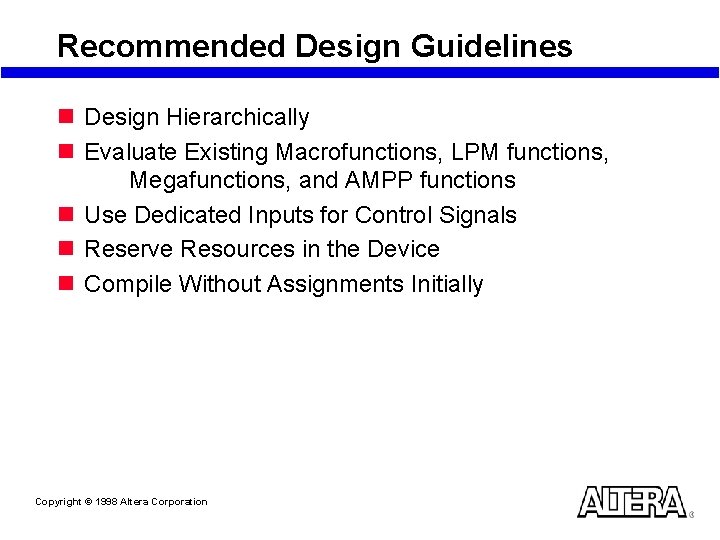
Recommended Design Guidelines n Design Hierarchically n Evaluate Existing Macrofunctions, LPM functions, Megafunctions, and AMPP functions n Use Dedicated Inputs for Control Signals n Reserve Resources in the Device n Compile Without Assignments Initially Copyright © 1998 Altera Corporation

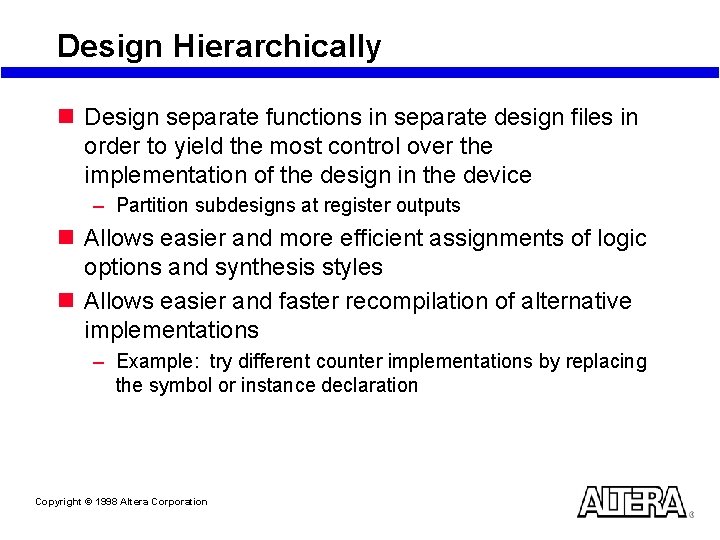
Design Hierarchically n Design separate functions in separate design files in order to yield the most control over the implementation of the design in the device – Partition subdesigns at register outputs n Allows easier and more efficient assignments of logic options and synthesis styles n Allows easier and faster recompilation of alternative implementations – Example: try different counter implementations by replacing the symbol or instance declaration Copyright © 1998 Altera Corporation

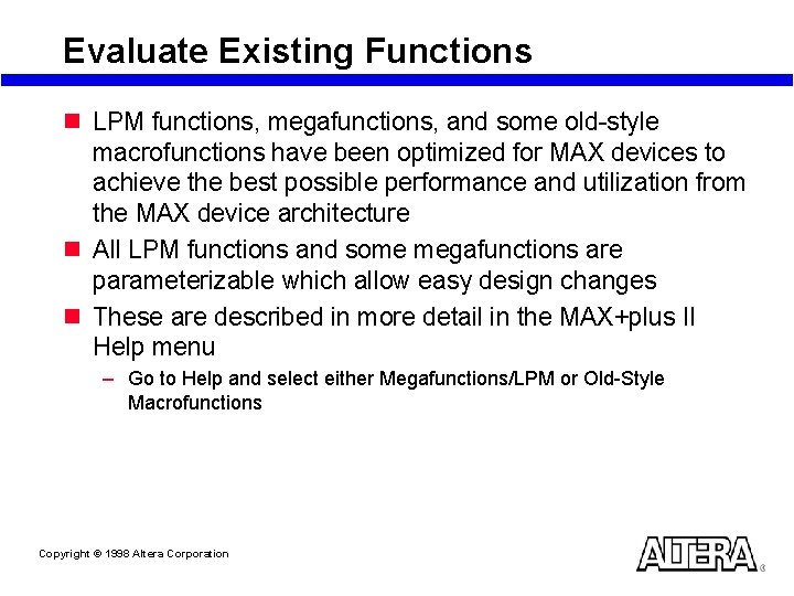
Evaluate Existing Functions n LPM functions, megafunctions, and some old-style macrofunctions have been optimized for MAX devices to achieve the best possible performance and utilization from the MAX device architecture n All LPM functions and some megafunctions are parameterizable which allow easy design changes n These are described in more detail in the MAX+plus II Help menu – Go to Help and select either Megafunctions/LPM or Old-Style Macrofunctions Copyright © 1998 Altera Corporation

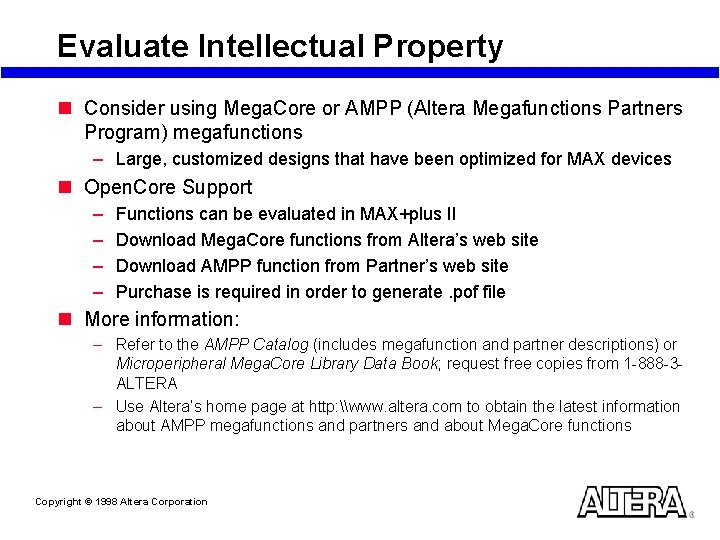
Evaluate Intellectual Property n Consider using Mega. Core or AMPP (Altera Megafunctions Partners Program) megafunctions – Large, customized designs that have been optimized for MAX devices n Open. Core Support – – Functions can be evaluated in MAX+plus II Download Mega. Core functions from Altera’s web site Download AMPP function from Partner’s web site Purchase is required in order to generate. pof file n More information: – Refer to the AMPP Catalog (includes megafunction and partner descriptions) or Microperipheral Mega. Core Library Data Book; request free copies from 1 -888 -3 ALTERA – Use Altera’s home page at http: \www. altera. com to obtain the latest information about AMPP megafunctions and partners and about Mega. Core functions Copyright © 1998 Altera Corporation

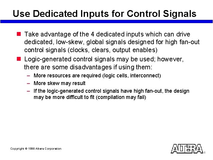
Use Dedicated Inputs for Control Signals n Take advantage of the 4 dedicated inputs which can drive dedicated, low-skew, global signals designed for high fan-out control signals (clocks, clears, output enables) n Logic-generated control signals may be used; however, there are some disadvantages if using them: – More resources are required (logic cells, interconnect) – More skew may result – If the logic-generated control signals have high fan-out, the design may be more difficult to fit (compilation may fail) Copyright © 1998 Altera Corporation

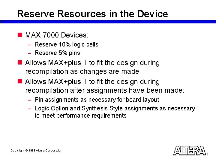
Reserve Resources in the Device n MAX 7000 Devices: – Reserve 10% logic cells – Reserve 5% pins n Allows MAX+plus II to fit the design during recompilation as changes are made n Allows MAX+plus II to fit the design during recompilation after assignments have been made: – Pin assignments as necessary for board layout – Logic Option and Synthesis Style assignments as necessary to meet performance requirements Copyright © 1998 Altera Corporation

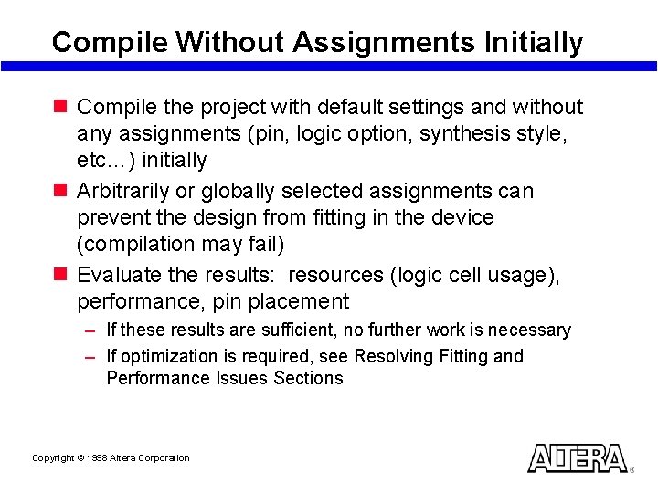
Compile Without Assignments Initially n Compile the project with default settings and without any assignments (pin, logic option, synthesis style, etc…) initially n Arbitrarily or globally selected assignments can prevent the design from fitting in the device (compilation may fail) n Evaluate the results: resources (logic cell usage), performance, pin placement – If these results are sufficient, no further work is necessary – If optimization is required, see Resolving Fitting and Performance Issues Sections Copyright © 1998 Altera Corporation

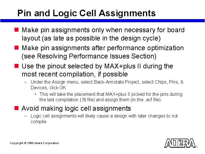
Pin and Logic Cell Assignments n Make pin assignments only when necessary for board layout (as late as possible in the design cycle) n Make pin assignments after performance optimization (see Resolving Performance Issues Section) n Use the pinout selected by MAX+plus II during the most recent compilation, if possible – Under the Assign menu, select Back-Annotate Project, select Chips, Pins, & Devices, click OK • This will take the placement that MAX+plus II picked for the pins during the last compilation (. fit file) and assign them (in the. acf file) n Avoid making logic cell assignments – Logic cell assignments will likely cause a design with later changes to not compile Copyright © 1998 Altera Corporation

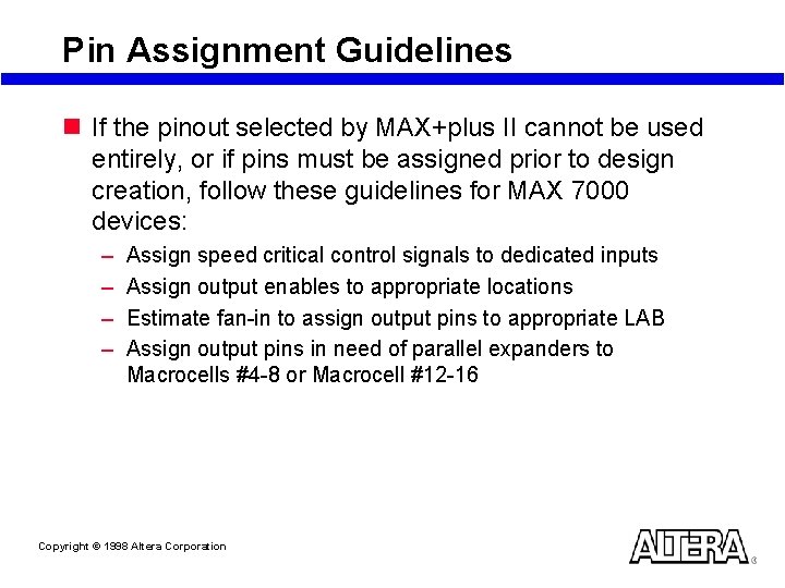
Pin Assignment Guidelines n If the pinout selected by MAX+plus II cannot be used entirely, or if pins must be assigned prior to design creation, follow these guidelines for MAX 7000 devices: – – Assign speed critical control signals to dedicated inputs Assign output enables to appropriate locations Estimate fan-in to assign output pins to appropriate LAB Assign output pins in need of parallel expanders to Macrocells #4 -8 or Macrocell #12 -16 Copyright © 1998 Altera Corporation

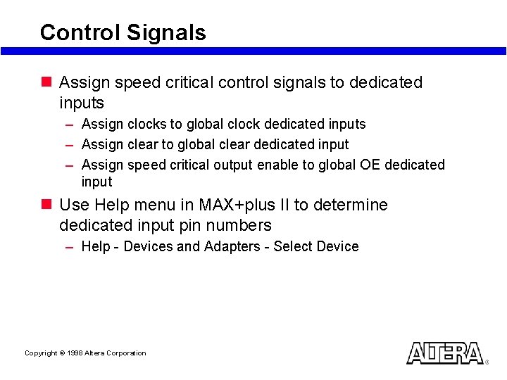
Control Signals n Assign speed critical control signals to dedicated inputs – Assign clocks to global clock dedicated inputs – Assign clear to global clear dedicated input – Assign speed critical output enable to global OE dedicated input n Use Help menu in MAX+plus II to determine dedicated input pin numbers – Help - Devices and Adapters - Select Device Copyright © 1998 Altera Corporation

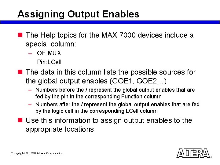
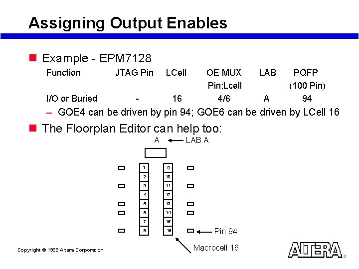
Assigning Output Enables n The Help topics for the MAX 7000 devices include a special column: – OE MUX Pin; LCell n The data in this column lists the possible sources for the global output enables (GOE 1, GOE 2…) – Numbers before the / represent the global output enables that are fed by the pin in the corresponding Function column – Numbers after the / represent the global output enables that are fed by the logic cell in the corresponding LCell column n Use this information to assign output enables to the appropriate locations Copyright © 1998 Altera Corporation

Assigning Output Enables n Example - EPM 7128 Function I/O or Buried JTAG Pin LCell - 16 OE MUX Pin; Lcell 4/6 LAB A PQFP (100 Pin) 94 – GOE 4 can be driven by pin 94; GOE 6 can be driven by LCell 16 n The Floorplan Editor can help too: A Copyright © 1998 Altera Corporation LAB A 1 9 2 10 3 11 4 12 5 13 6 14 7 15 8 16 Pin 94 Macrocell 16

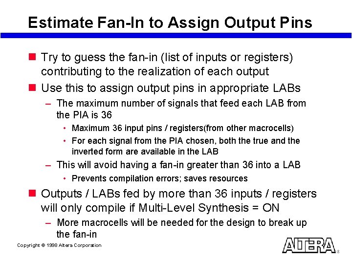
Estimate Fan-In to Assign Output Pins n Try to guess the fan-in (list of inputs or registers) contributing to the realization of each output n Use this to assign output pins in appropriate LABs – The maximum number of signals that feed each LAB from the PIA is 36 • Maximum 36 input pins / registers(from other macrocells) • For each signal from the PIA chosen, both the true and the inverted form are available in the LAB – This will avoid having a fan-in greater than 36 into a LAB • Prevents compilation errors; saves resources n Outputs / LABs fed by more than 36 inputs / registers will only compile if Multi-Level Synthesis = ON – More macrocells will be needed for the design to break up the fan-in Copyright © 1998 Altera Corporation

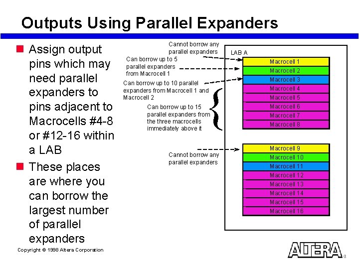
Outputs Using Parallel Expanders n Assign output pins which may need parallel expanders to pins adjacent to Macrocells #4 -8 or #12 -16 within a LAB n These places are where you can borrow the largest number of parallel expanders Copyright © 1998 Altera Corporation Cannot borrow any parallel expanders Can borrow up to 5 parallel expanders from Macrocell 1 { Can borrow up to 10 parallel expanders from Macrocell 1 and Macrocell 2 Can borrow up to 15 parallel expanders from the three macrocells immediately above it Cannot borrow any parallel expanders LAB A Macrocell 1 Macrocell 2 Macrocell 3 Macrocell 4 Macrocell 5 Macrocell 6 Macrocell 7 Macrocell 8 Macrocell 9 Macrocell 10 Macrocell 11 Macrocell 12 Macrocell 13 Macrocell 14 Macrocell 15 Macrocell 16

Altera Design Methodology Resolving Fitting Issues Copyright © 1998 Altera Corporation

Topics n Compiling a design in MAX+PLUS II n Resolving macrocell usage issues n Resolving routing issues Copyright © 1998 Altera Corporation

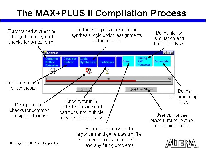
The MAX+PLUS II Compilation Process Performs logic synthesis using synthesis logic option assignments in the. acf file Extracts netlist of entire design hierarchy and checks for syntax error Builds database for synthesis Design Doctor checks for common design violations Checks for fit in selected device and partitions into multiple devices if necessary Copyright © 1998 Altera Corporation Executes place & route algorithm and generates. rpt file summarizing device utilization and any fitting problems Builds file for simulation and timing analysis Builds programming files User can pause place & route routine to examine status

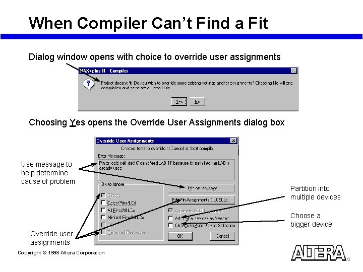
When Compiler Can’t Find a Fit Dialog window opens with choice to override user assignments Choosing Yes opens the Override User Assignments dialog box Use message to help determine cause of problem Partition into multiple devices Choose a bigger device Override user assignments Copyright © 1998 Altera Corporation

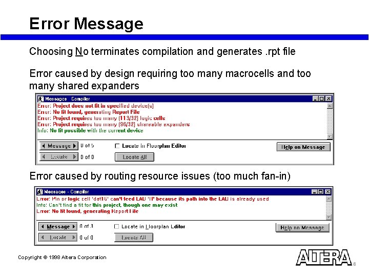
Error Message Choosing No terminates compilation and generates. rpt file Error caused by design requiring too many macrocells and too many shared expanders Error caused by routing resource issues (too much fan-in) Copyright © 1998 Altera Corporation

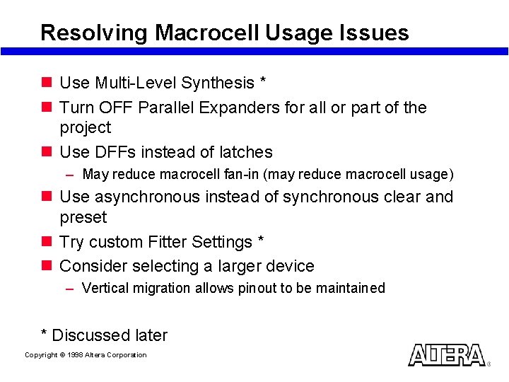
Resolving Macrocell Usage Issues n Use Multi-Level Synthesis * n Turn OFF Parallel Expanders for all or part of the project n Use DFFs instead of latches – May reduce macrocell fan-in (may reduce macrocell usage) n Use asynchronous instead of synchronous clear and preset n Try custom Fitter Settings * n Consider selecting a larger device – Vertical migration allows pinout to be maintained * Discussed later Copyright © 1998 Altera Corporation

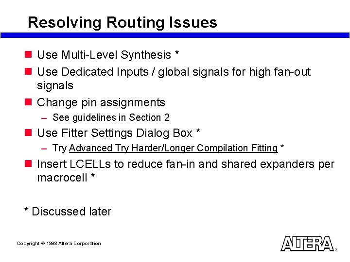
Resolving Routing Issues n Use Multi-Level Synthesis * n Use Dedicated Inputs / global signals for high fan-out signals n Change pin assignments – See guidelines in Section 2 n Use Fitter Settings Dialog Box * – Try Advanced Try Harder/Longer Compilation Fitting * n Insert LCELLs to reduce fan-in and shared expanders per macrocell * * Discussed later Copyright © 1998 Altera Corporation

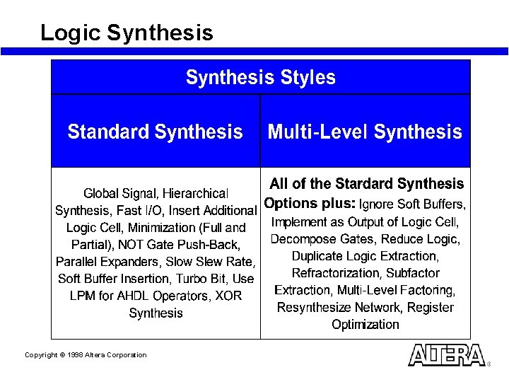
Logic Synthesis Copyright © 1998 Altera Corporation

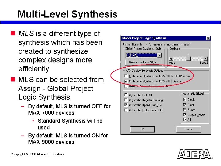
Multi-Level Synthesis n MLS is a different type of synthesis which has been created to synthesize complex designs more efficiently n MLS can be selected from Assign - Global Project Logic Synthesis – By default, MLS is turned OFF for MAX 7000 devices • Standard Synthesis will be used – By default, MLS is turned ON for MAX 9000 devices Copyright © 1998 Altera Corporation

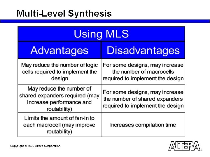
Multi-Level Synthesis Copyright © 1998 Altera Corporation

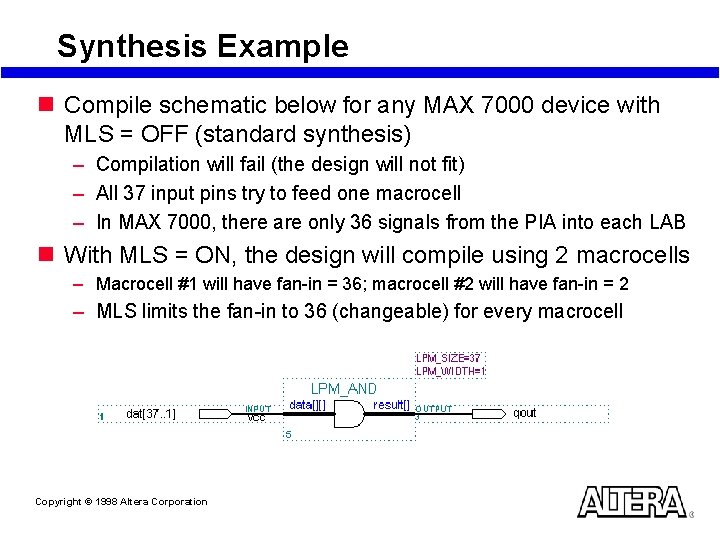
Synthesis Example n Compile schematic below for any MAX 7000 device with MLS = OFF (standard synthesis) – Compilation will fail (the design will not fit) – All 37 input pins try to feed one macrocell – In MAX 7000, there are only 36 signals from the PIA into each LAB n With MLS = ON, the design will compile using 2 macrocells – Macrocell #1 will have fan-in = 36; macrocell #2 will have fan-in = 2 – MLS limits the fan-in to 36 (changeable) for every macrocell Copyright © 1998 Altera Corporation

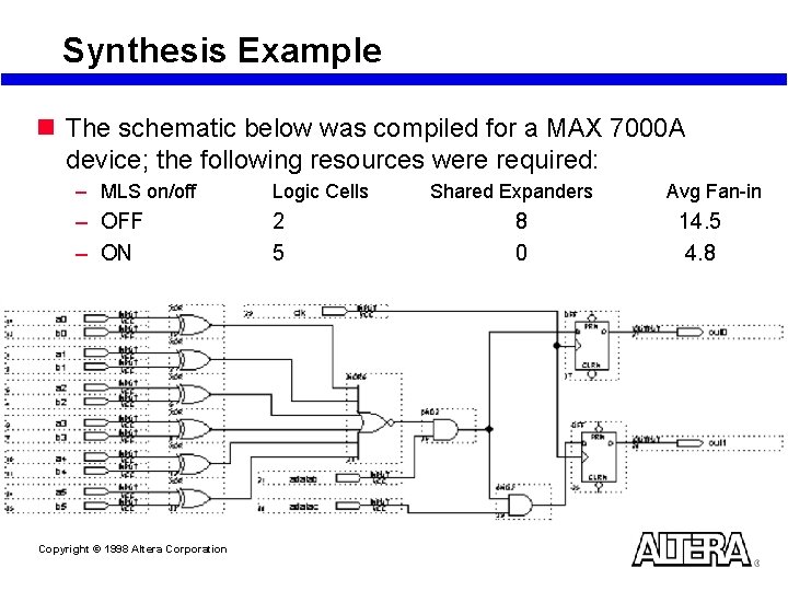
Synthesis Example n The schematic below was compiled for a MAX 7000 A device; the following resources were required: – MLS on/off Logic Cells – OFF – ON 2 5 Copyright © 1998 Altera Corporation Shared Expanders 8 0 Avg Fan-in 14. 5 4. 8

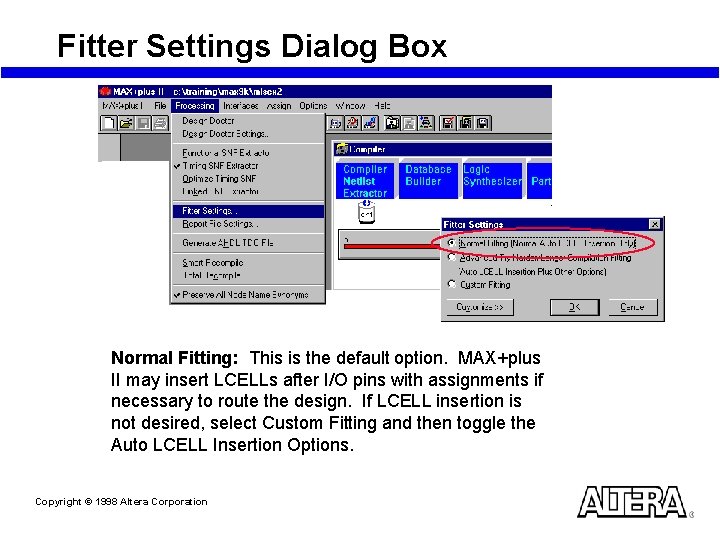
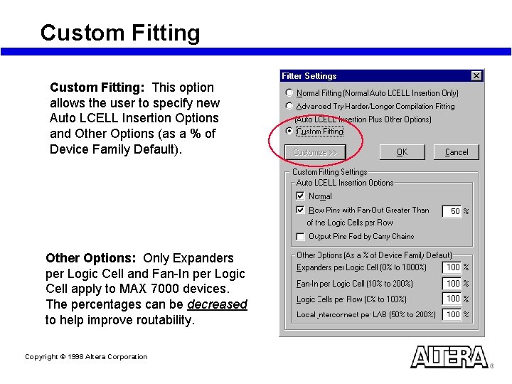
Fitter Settings Dialog Box Normal Fitting: This is the default option. MAX+plus II may insert LCELLs after I/O pins with assignments if necessary to route the design. If LCELL insertion is not desired, select Custom Fitting and then toggle the Auto LCELL Insertion Options. Copyright © 1998 Altera Corporation

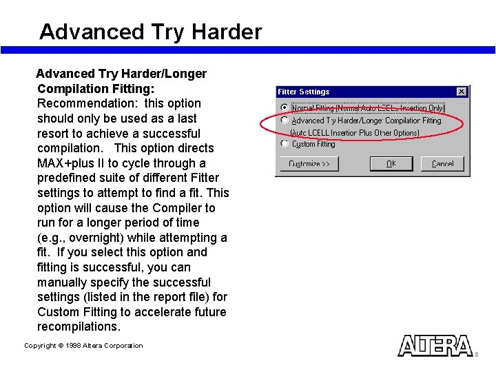
Advanced Try Harder/Longer Compilation Fitting: Recommendation: this option should only be used as a last resort to achieve a successful compilation. This option directs MAX+plus II to cycle through a predefined suite of different Fitter settings to attempt to find a fit. This option will cause the Compiler to run for a longer period of time (e. g. , overnight) while attempting a fit. If you select this option and fitting is successful, you can manually specify the successful settings (listed in the report file) for Custom Fitting to accelerate future recompilations. Copyright © 1998 Altera Corporation

Custom Fitting: This option allows the user to specify new Auto LCELL Insertion Options and Other Options (as a % of Device Family Default). Other Options: Only Expanders per Logic Cell and Fan-In per Logic Cell apply to MAX 7000 devices. The percentages can be decreased to help improve routability. Copyright © 1998 Altera Corporation

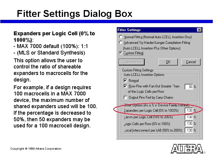
Fitter Settings Dialog Box Expanders per Logic Cell (0% to 1000%): - MAX 7000 default (100%): 1: 1 - (MLS or Standard Synthesis) This option allows the user to control the ratio of shareable expanders to macrocells for the design. For example, if a design requires 100 macrocells in a MAX 7000 device, the maximum number of shared expanders used will be 100. If the percentage is decreased to 50%, then 50 expanders may be used for a 100 macrocell design. Copyright © 1998 Altera Corporation

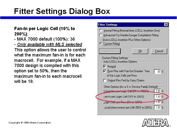
Fitter Settings Dialog Box Fan-In per Logic Cell (10% to 200%): - MAX 7000 default (100%): 36 - Only available with MLS selected This option allows the user to control what the maximum fan-in is for each macrocell. For example, if a MAX 7000 design is compiled with this option set to 50%, then the maximum fan-in to each macrocell will be 18. Copyright © 1998 Altera Corporation

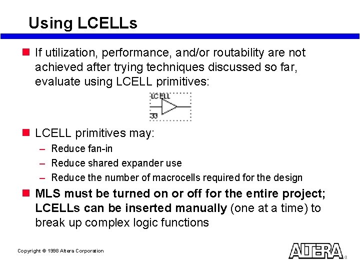
Using LCELLs n If utilization, performance, and/or routability are not achieved after trying techniques discussed so far, evaluate using LCELL primitives: n LCELL primitives may: – Reduce fan-in – Reduce shared expander use – Reduce the number of macrocells required for the design n MLS must be turned on or off for the entire project; LCELLs can be inserted manually (one at a time) to break up complex logic functions Copyright © 1998 Altera Corporation

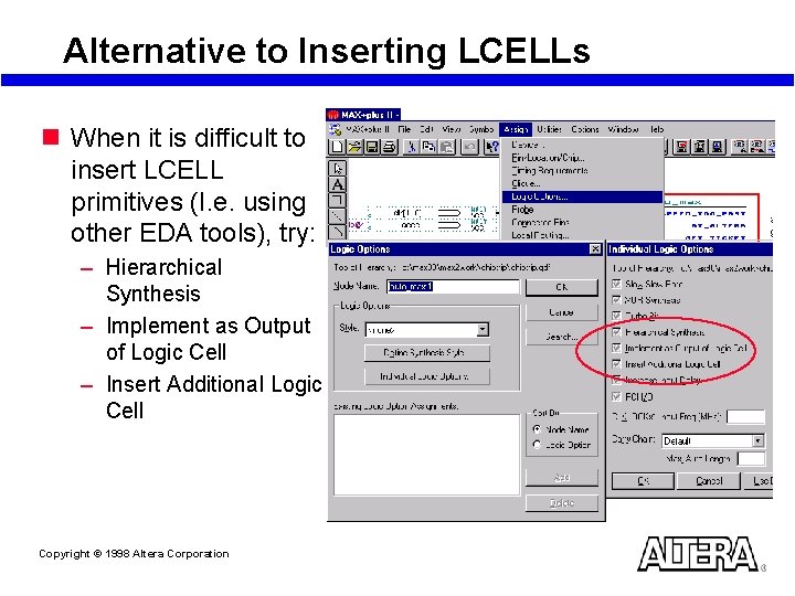
Alternative to Inserting LCELLs n When it is difficult to insert LCELL primitives (I. e. using other EDA tools), try: – Hierarchical Synthesis – Implement as Output of Logic Cell – Insert Additional Logic Cell Copyright © 1998 Altera Corporation

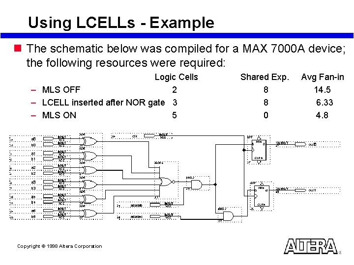
Using LCELLs - Example n The schematic below was compiled for a MAX 7000 A device; the following resources were required: Logic Cells – MLS OFF 2 – LCELL inserted after NOR gate 3 – MLS ON 5 Copyright © 1998 Altera Corporation Shared Exp. 8 8 0 Avg Fan-in 14. 5 6. 33 4. 8

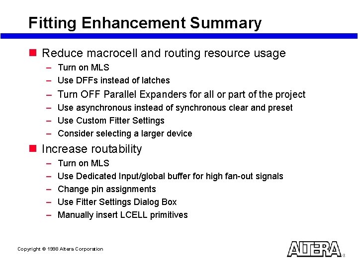
Fitting Enhancement Summary n Reduce macrocell and routing resource usage – Turn on MLS – Use DFFs instead of latches – Turn OFF Parallel Expanders for all or part of the project – Use asynchronous instead of synchronous clear and preset – Use Custom Fitter Settings – Consider selecting a larger device n Increase routability – – – Turn on MLS Use Dedicated Input/global buffer for high fan-out signals Change pin assignments Use Fitter Settings Dialog Box Manually insert LCELL primitives Copyright © 1998 Altera Corporation

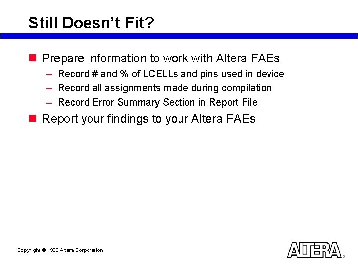
Still Doesn’t Fit? n Prepare information to work with Altera FAEs – Record # and % of LCELLs and pins used in device – Record all assignments made during compilation – Record Error Summary Section in Report File n Report your findings to your Altera FAEs Copyright © 1998 Altera Corporation

Laboratory Exercise 2 Go to Laboratory Exercise Manual and Complete Exercise 2 Copyright © 1998 Altera Corporation

Altera Design Methodology Resolving Performance Issues Copyright © 1998 Altera Corporation

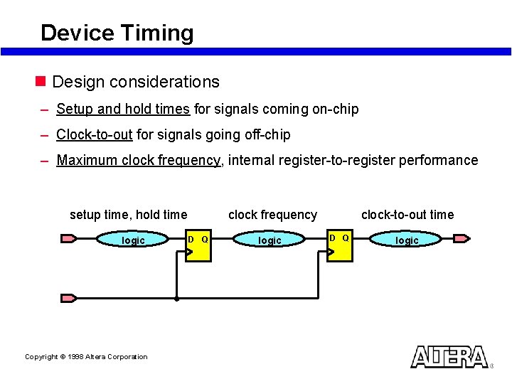
Device Timing n Design considerations – Setup and hold times for signals coming on-chip – Clock-to-out for signals going off-chip – Maximum clock frequency, internal register-to-register performance setup time, hold time logic Copyright © 1998 Altera Corporation clock frequency D Q logic clock-to-out time D Q logic

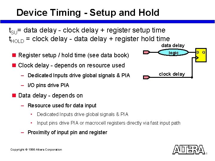
Device Timing - Setup and Hold t. SU= data delay - clock delay + register setup time t. HOLD = clock delay - data delay + register hold time data delay n Register setup / hold time (see data book) logic n Clock delay - depends on resource used – Dedicated Inputs drive global signals & PIA clock delay – I/O pins drive PIA n Data delay - depends on – Resource used for data input • Dedicated Inputs drive global signals & PIA • Input pins drive PIA or macrocell registers directly via fast input path – Proximity of input pin and register Copyright © 1998 Altera Corporation D Q

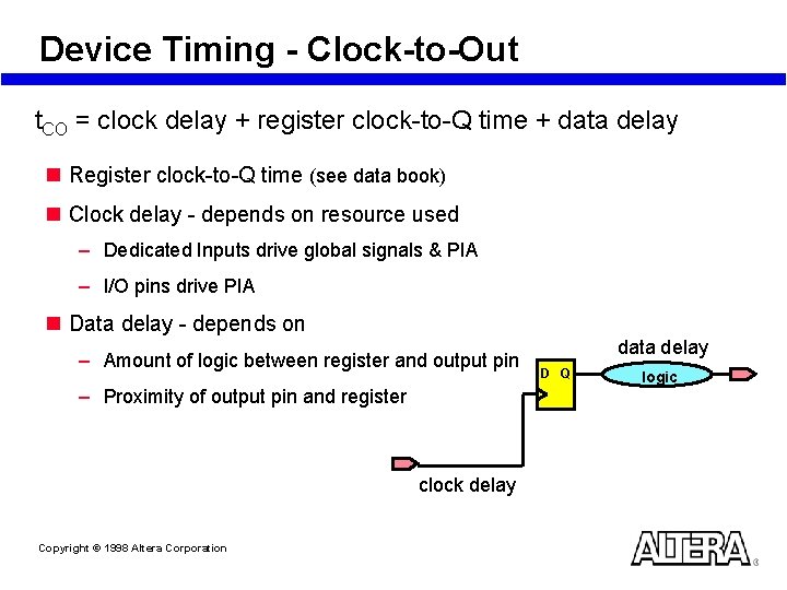
Device Timing - Clock-to-Out t. CO = clock delay + register clock-to-Q time + data delay n Register clock-to-Q time (see data book) n Clock delay - depends on resource used – Dedicated Inputs drive global signals & PIA – I/O pins drive PIA n Data delay - depends on – Amount of logic between register and output pin – Proximity of output pin and register clock delay Copyright © 1998 Altera Corporation data delay D Q logic

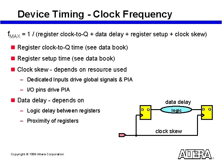
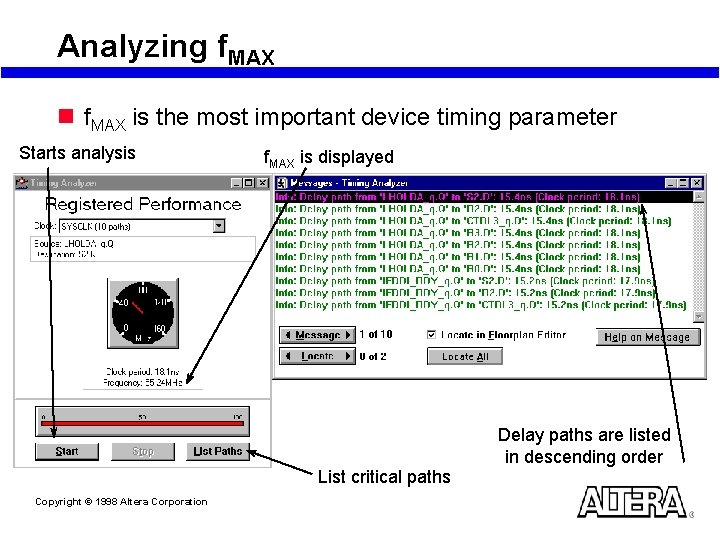
Device Timing - Clock Frequency f. MAX = 1 / (register clock-to-Q + data delay + register setup + clock skew) n Register clock-to-Q time (see data book) n Register setup time (see data book) n Clock skew - depends on resource used – Dedicated Inputs drive global signals & PIA – I/O pins drive PIA n Data delay - depends on – Logic delay between registers data delay D Q logic – Proximity of registers clock skew Copyright © 1998 Altera Corporation D Q

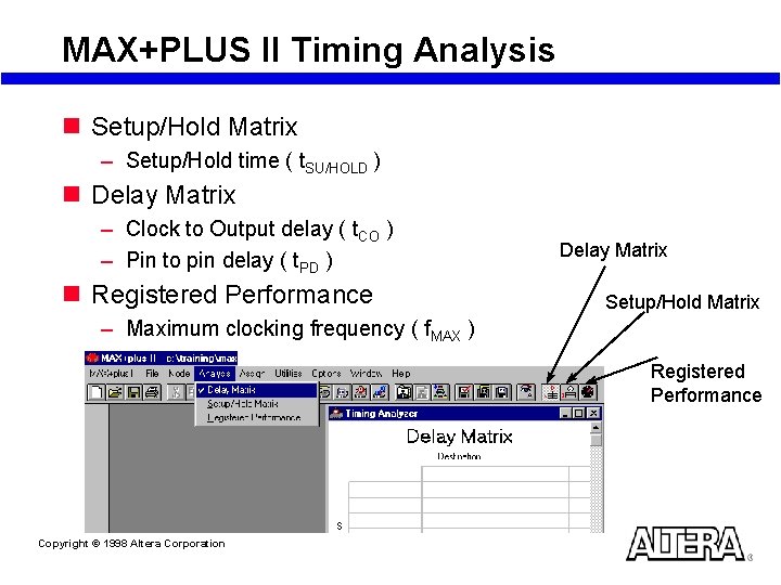
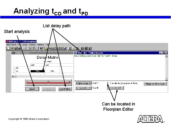
MAX+PLUS II Timing Analysis n Setup/Hold Matrix – Setup/Hold time ( t. SU/HOLD ) n Delay Matrix – Clock to Output delay ( t. CO ) – Pin to pin delay ( t. PD ) n Registered Performance Delay Matrix Setup/Hold Matrix – Maximum clocking frequency ( f. MAX ) Registered Performance Copyright © 1998 Altera Corporation

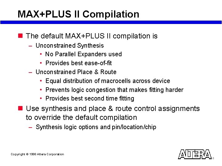
MAX+PLUS II Compilation n The default MAX+PLUS II compilation is – Unconstrained Synthesis • No Parallel Expanders used • Provides best ease-of-fit – Unconstrained Place & Route • Equal distribution of macrocells across device • Prevents logic congestion that makes fitting harder • Provides best second time fitting n Use synthesis and place & route control assignments to override the default compilation – Synthesis logic options and pin/location/chip Copyright © 1998 Altera Corporation

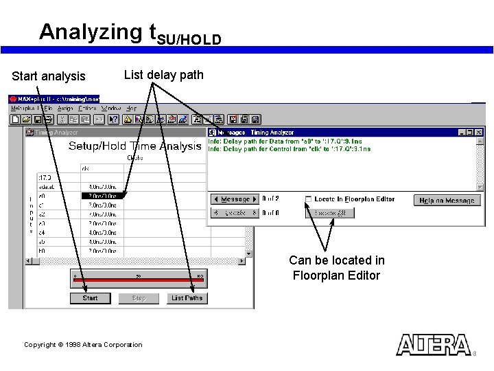
Analyzing t. SU/HOLD Start analysis List delay path Can be located in Floorplan Editor Copyright © 1998 Altera Corporation

Analyzing t. CO and t. PD List delay path Start analysis Can be located in Floorplan Editor Copyright © 1998 Altera Corporation

Analyzing f. MAX n f. MAX is the most important device timing parameter Starts analysis f. MAX is displayed Delay paths are listed in descending order List critical paths Copyright © 1998 Altera Corporation

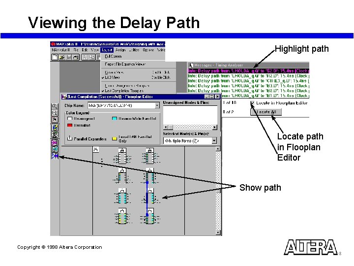
Viewing the Delay Path Highlight path Locate path in Flooplan Editor Show path Copyright © 1998 Altera Corporation

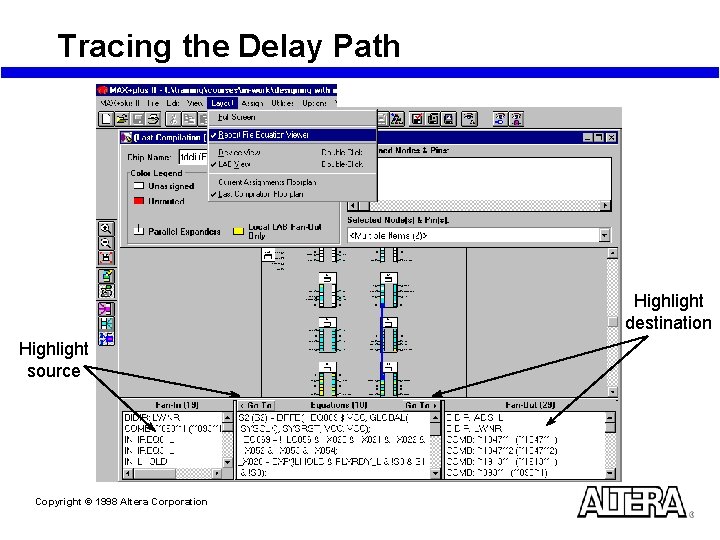
Tracing the Delay Path Highlight destination Highlight source Copyright © 1998 Altera Corporation

Achieving Performance in MAX 7000 Copyright © 1998 Altera Corporation

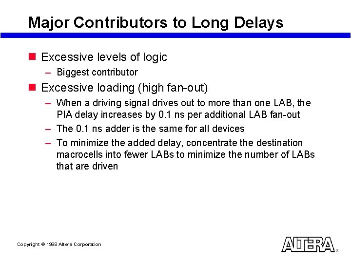
Major Contributors to Long Delays n Excessive levels of logic – Biggest contributor n Excessive loading (high fan-out) – When a driving signal drives out to more than one LAB, the PIA delay increases by 0. 1 ns per additional LAB fan-out – The 0. 1 ns adder is the same for all devices – To minimize the added delay, concentrate the destination macrocells into fewer LABs to minimize the number of LABs that are driven Copyright © 1998 Altera Corporation

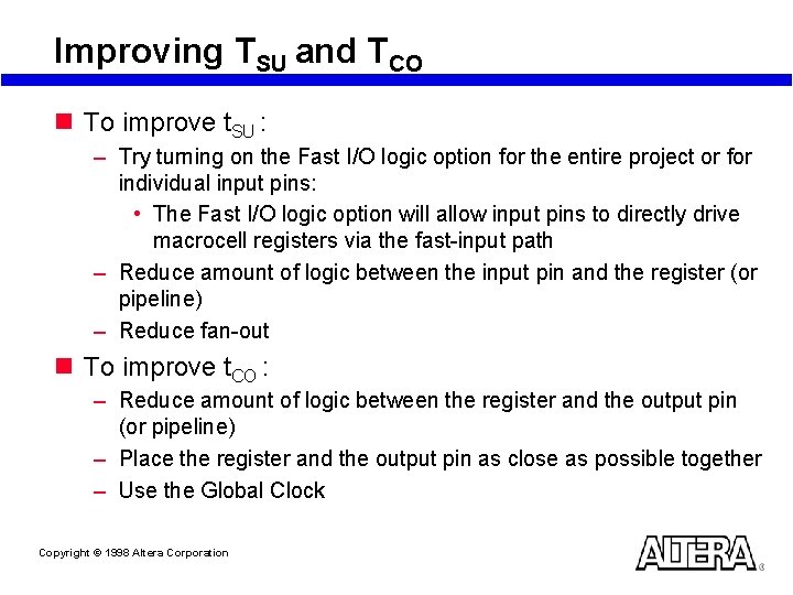
Improving TSU and TCO n To improve t. SU : – Try turning on the Fast I/O logic option for the entire project or for individual input pins: • The Fast I/O logic option will allow input pins to directly drive macrocell registers via the fast-input path – Reduce amount of logic between the input pin and the register (or pipeline) – Reduce fan-out n To improve t. CO : – Reduce amount of logic between the register and the output pin (or pipeline) – Place the register and the output pin as close as possible together – Use the Global Clock Copyright © 1998 Altera Corporation

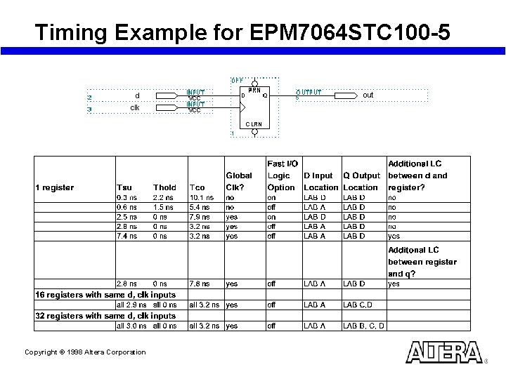
Timing Example for EPM 7064 STC 100 -5 Copyright © 1998 Altera Corporation

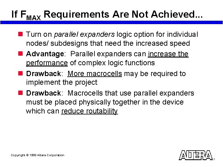
If FMAX Requirements Are Not Achieved. . . n Turn on parallel expanders logic option for individual nodes/ subdesigns that need the increased speed n Advantage: Parallel expanders can increase the performance of complex logic functions n Drawback: More macrocells may be required to implement the project n Drawback: Macrocells that use parallel expanders must be placed physically together in the device which can reduce routability Copyright © 1998 Altera Corporation

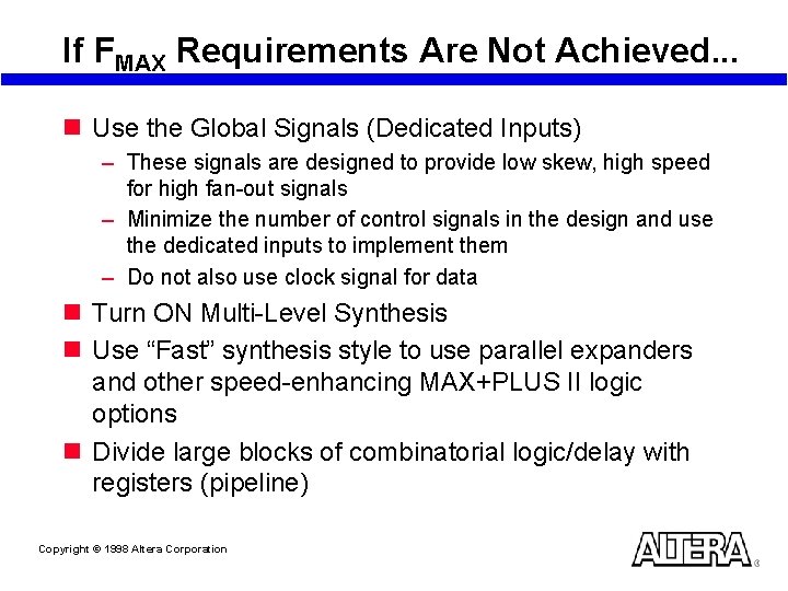
If FMAX Requirements Are Not Achieved. . . n Use the Global Signals (Dedicated Inputs) – These signals are designed to provide low skew, high speed for high fan-out signals – Minimize the number of control signals in the design and use the dedicated inputs to implement them – Do not also use clock signal for data n Turn ON Multi-Level Synthesis n Use “Fast” synthesis style to use parallel expanders and other speed-enhancing MAX+PLUS II logic options n Divide large blocks of combinatorial logic/delay with registers (pipeline) Copyright © 1998 Altera Corporation

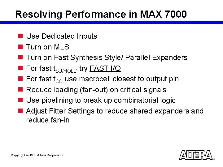
Resolving Performance in MAX 7000 n n n n Use Dedicated Inputs Turn on MLS Turn on Fast Synthesis Style/ Parallel Expanders For fast t. SU/HOLD try FAST I/O For fast t. CO use macrocell closest to output pin Reduce loading (fan-out) on critical signals Use pipelining to break up combinatorial logic Adjust Fitter Settings to reduce shared expanders and reduce fan-in Copyright © 1998 Altera Corporation

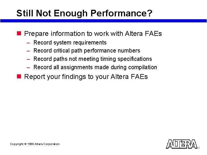
Still Not Enough Performance? n Prepare information to work with Altera FAEs – – Record system requirements Record critical path performance numbers Record paths not meeting timing specifications Record all assignments made during compilation n Report your findings to your Altera FAEs Copyright © 1998 Altera Corporation

Laboratory Exercise 3 Go to Laboratory Exercise Manual and Complete Exercise 3 Copyright © 1998 Altera Corporation

SECTION 4 Programming MAX 7000 Devices Copyright © 1998 Altera Corporation

SECTION 4 Outline n Programming Overview n Using Download Cables – Laboratory Exercise #4 n Using In-Circuit Testers n Using an Embedded Processor n In-System Programming Times Copyright © 1998 Altera Corporation

Programming Overview Copyright © 1998 Altera Corporation

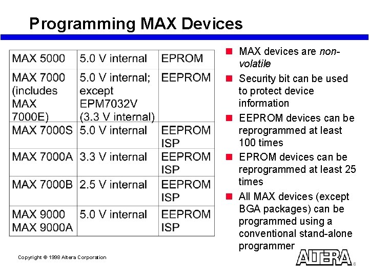
Programming MAX Devices n MAX devices are nonvolatile n Security bit can be used to protect device information n EEPROM devices can be reprogrammed at least 100 times n EPROM devices can be reprogrammed at least 25 times n All MAX devices (except BGA packages) can be programmed using a conventional stand-alone programmer Copyright © 1998 Altera Corporation

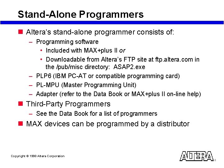
Stand-Alone Programmers n Altera’s stand-alone programmer consists of: – Programming software • Included with MAX+plus II or • Downloadable from Altera’s FTP site at ftp. altera. com in the /pub/misc directory: ASAP 2. exe – PLP 6 (IBM PC-AT or compatible programming card) – PL-MPU (Master Programming Unit) – Adapter (refer to the Data Book or MAX+plus II on-line help) n Third-Party Programmers – See the Data Book for a list of programmers n MAX devices can be programmed by a distributor Copyright © 1998 Altera Corporation

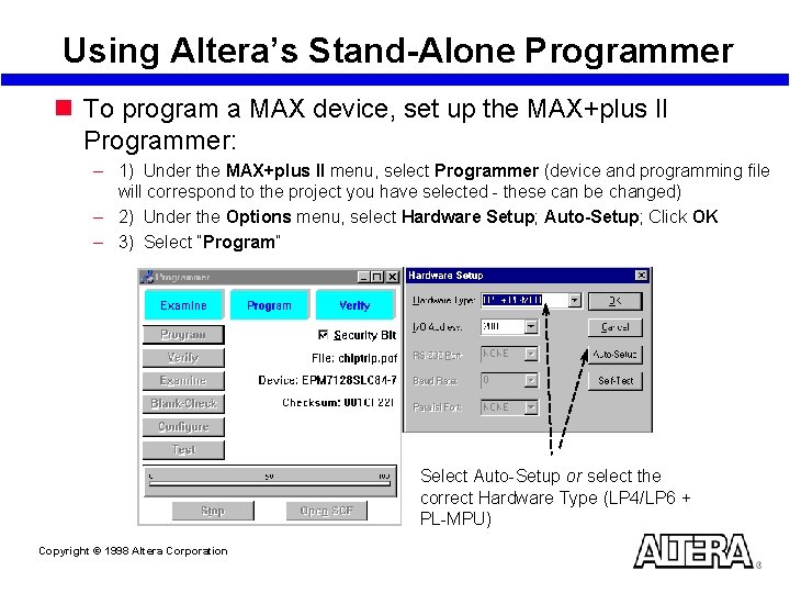
Using Altera’s Stand-Alone Programmer n To program a MAX device, set up the MAX+plus II Programmer: – 1) Under the MAX+plus II menu, select Programmer (device and programming file will correspond to the project you have selected - these can be changed) – 2) Under the Options menu, select Hardware Setup; Auto-Setup; Click OK – 3) Select “Program” Select Auto-Setup or select the correct Hardware Type (LP 4/LP 6 + PL-MPU) Copyright © 1998 Altera Corporation

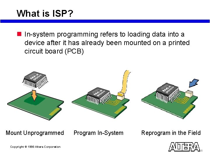
What is ISP? n In-system programming refers to loading data into a device after it has already been mounted on a printed circuit board (PCB) Mount Unprogrammed Copyright © 1998 Altera Corporation Program In-System Reprogram in the Field

ISP Benefits n Minimizes cost – Sockets no longer needed – Removes stand alone programming methodology n Minimizes device handling – Prevents bent leads (most important for delicate QFP packages) – Reduces possibility of ESD damage n Easy Prototyping n Improves manufacturing efficiency – Integrated programming & testing using in-circuit testers – No longer necessary to keep inventory of programmed devices n Easy field upgrades – Design changes downloaded to system in the field quickly – No need to return system for upgrades Copyright © 1998 Altera Corporation

Using IEEE Std. 1149. 1 JTAG Test Port n ISP through Joint Test Action Group (JTAG) test port is the industry standard n Ease of use – Devices in the JTAG chain can be in-system programmed and tested with in-circuit testers – All JTAG/ISP devices on board can be programmed using the same hardware – Supports concurrent programming • Concurrent programming supported within a device family • Programming time for JTAG chain is on the order of the time for the biggest device in the chain Copyright © 1998 Altera Corporation

Enabling JTAG Support Copyright © 1998 Altera Corporation

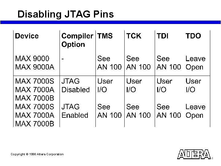
Disabling JTAG Pins Copyright © 1998 Altera Corporation

MAX 7000 AE Enhanced ISP Features n New ISP programming algorithm (simplified) – Fewer instructions and addressing information • Auto-increment counter added to supply addresses – Improves programming by a factor of 2 to 10 times n ISP Done Bit – Last bit programmed – Prevents I/Os from driving out if ISP is interrupted n Pull-up resistor on I/O pins during ISP – Allows for bus friendly interface Copyright © 1998 Altera Corporation

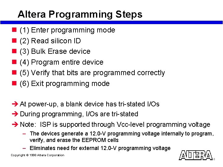
Altera Programming Steps n n n (1) Enter programming mode (2) Read silicon ID (3) Bulk Erase device (4) Program entire device (5) Verify that bits are programmed correctly (6) Exit programming mode è At power-up, a blank device has tri-stated I/Os è During programming, I/Os are tri-stated è Note: ISP is supported through Vcc-level programming voltage – The devices generate a 12. 0 -V programming voltage internally to program, verify, and erase the EEPROM cells – Eliminates need for external 12. 0 -V programming voltage Copyright © 1998 Altera Corporation

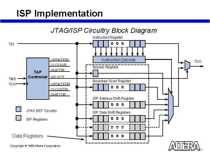
ISP Implementation JTAG/ISP Circuitry Block Diagram Instruction Register TDI UPDATEIR CLOCKIR SHIFTIR TMS TCK TAP Controller SELECT UPDATEDR CLOCKDR SHIFTDR JTAG BST Circuitry ISP Registers Data Registers Copyright © 1998 Altera Corporation Instruction Decode Bypass Register Boundary-Scan Register ISP Address Shift Register ISP Data Shift Registers TDO

ISP Implementation JTAG/ISP Circuitry Block Diagram n (1) Using the circuitry for JTAG Boundary-Scan Testing – Used to test for opens and shorts on pins – Supports BYPASS and other Boundary Scan modes – See AN 39 (JTAG Boundary-Scan Testing in Altera Devices) n (2) Using the circuitry for In-System Programming – – – ISP Instructions (Proprietary) TDI shifts in an instruction to Instruction Registers TDI shifts in an ISP address to ISP Address Registers TDI shifts in ISP data to ISP Data Registers The TAP Controller is a state machine that selects/enables the correct type of registers at the right time Copyright © 1998 Altera Corporation

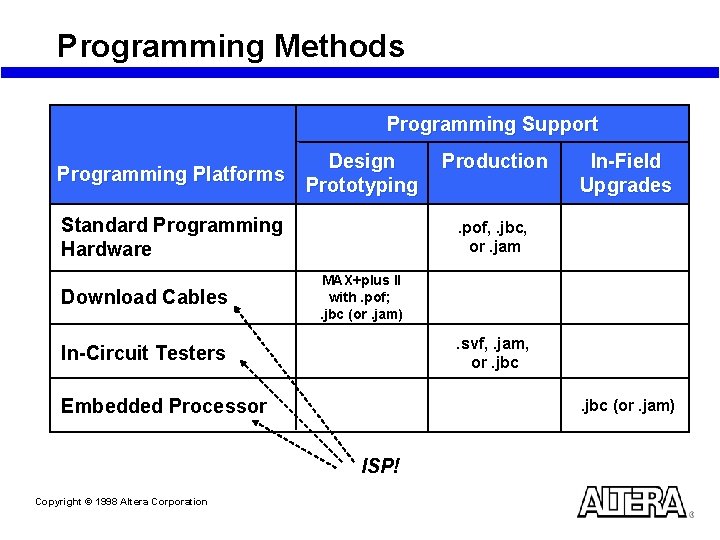
Programming Methods Programming Support Programming Platforms Design Prototyping Standard Programming Hardware Download Cables In-Field Upgrades . pof, . jbc, or. jam MAX+plus II with. pof; . jbc (or. jam) . svf, . jam, or. jbc In-Circuit Testers Embedded Processor . jbc (or. jam) ISP! Copyright © 1998 Altera Corporation Production

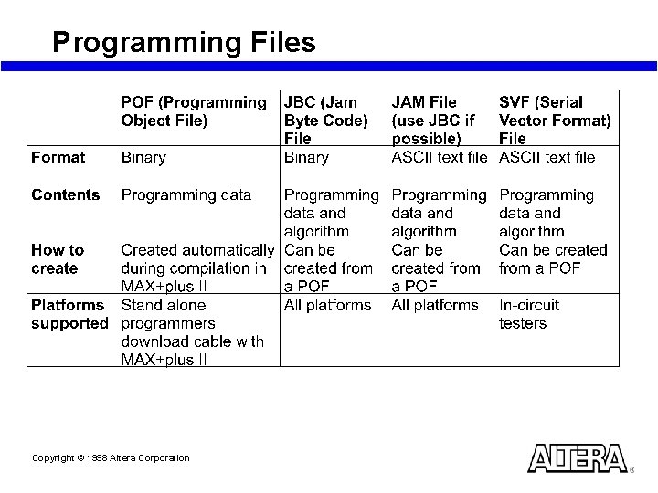
Programming Files Copyright © 1998 Altera Corporation

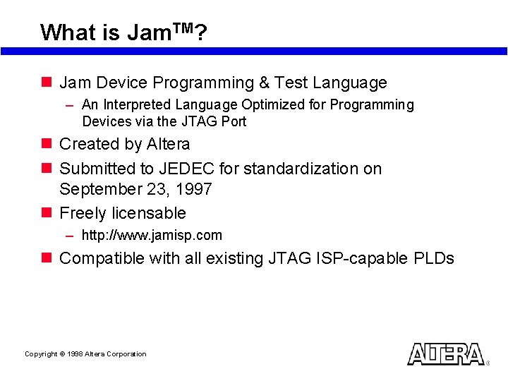
What is Jam. TM? n Jam Device Programming & Test Language – An Interpreted Language Optimized for Programming Devices via the JTAG Port n Created by Altera n Submitted to JEDEC for standardization on September 23, 1997 n Freely licensable – http: //www. jamisp. com n Compatible with all existing JTAG ISP-capable PLDs Copyright © 1998 Altera Corporation

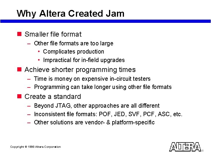
Why Altera Created Jam n Smaller file format – Other file formats are too large • Complicates production • Impractical for in-field upgrades n Achieve shorter programming times – Time is money on expensive in-circuit testers – Programming can take longer using other file formats n Create a standard – Beyond JTAG, other approaches are all different – Inconsistent file formats: POF, JED, SVF, PCF, ASC, etc. – Other solutions are vendor- & platform-specific Copyright © 1998 Altera Corporation

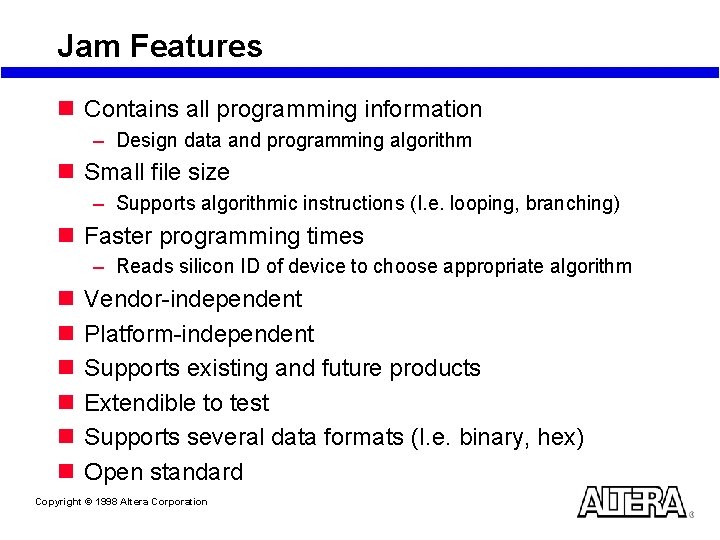
Jam Features n Contains all programming information – Design data and programming algorithm n Small file size – Supports algorithmic instructions (I. e. looping, branching) n Faster programming times – Reads silicon ID of device to choose appropriate algorithm n n n Vendor-independent Platform-independent Supports existing and future products Extendible to test Supports several data formats (I. e. binary, hex) Open standard Copyright © 1998 Altera Corporation

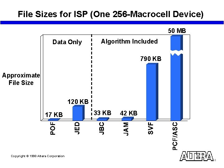
File Sizes for ISP (One 256 -Macrocell Device) 50 MB Data Only Algorithm Included 790 KB Approximate File Size 120 KB 17 KB Copyright © 1998 Altera Corporation 33 KB 42 KB

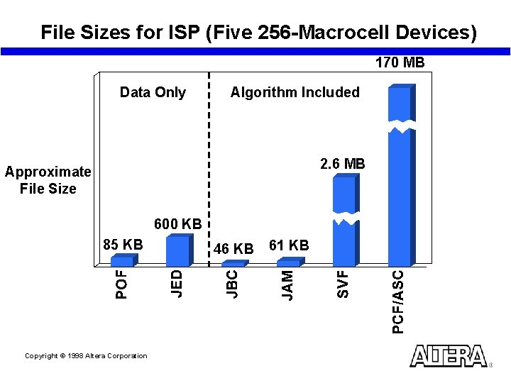
File Sizes for ISP (Five 256 -Macrocell Devices) 170 MB Data Only Algorithm Included 2. 6 MB Approximate File Size 600 KB 85 KB Copyright © 1998 Altera Corporation 46 KB 61 KB

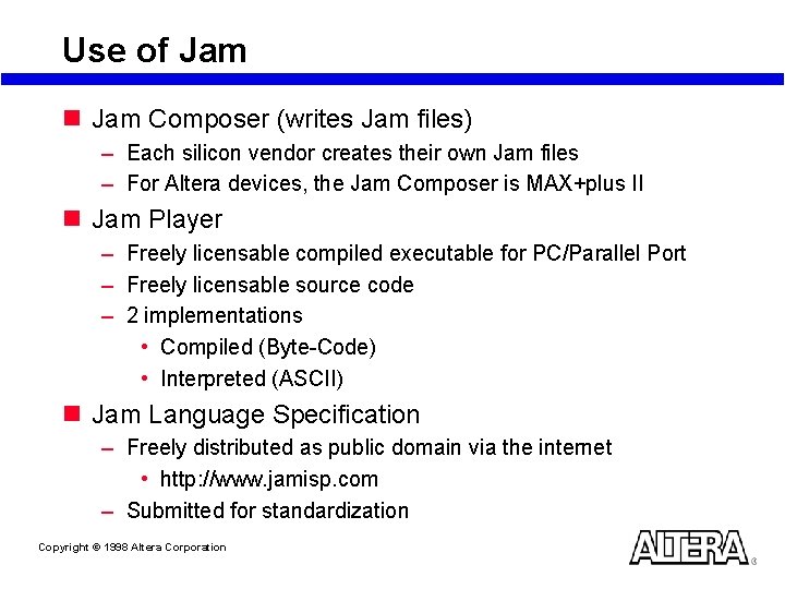
Use of Jam n Jam Composer (writes Jam files) – Each silicon vendor creates their own Jam files – For Altera devices, the Jam Composer is MAX+plus II n Jam Player – Freely licensable compiled executable for PC/Parallel Port – Freely licensable source code – 2 implementations • Compiled (Byte-Code) • Interpreted (ASCII) n Jam Language Specification – Freely distributed as public domain via the internet • http: //www. jamisp. com – Submitted for standardization Copyright © 1998 Altera Corporation

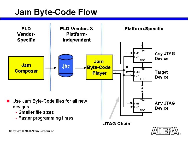
Jam Byte-Code Flow PLD Vendor. Specific Platform-Specific PLD Vendor- & Platform. Independent TMS TCK Jam Composer . jbc Jam Byte-Code Player TDI TDO TMS TCK TDI TDO n Use Jam Byte-Code files for all new designs - Smaller file sizes - Faster programming times TDI TMS TCK TDO JTAG Chain Copyright © 1998 Altera Corporation Any JTAG Device Target Device Any JTAG Device

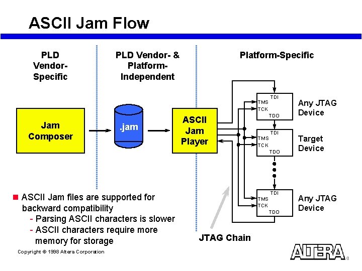
ASCII Jam Flow PLD Vendor. Specific Platform-Specific PLD Vendor- & Platform. Independent TMS TCK Jam Composer . jam ASCII Jam Player TDI TDO TMS TCK TDI TDO n ASCII Jam files are supported for backward compatibility - Parsing ASCII characters is slower - ASCII characters require more memory for storage Copyright © 1998 Altera Corporation TDI TMS TCK TDO JTAG Chain Any JTAG Device Target Device Any JTAG Device

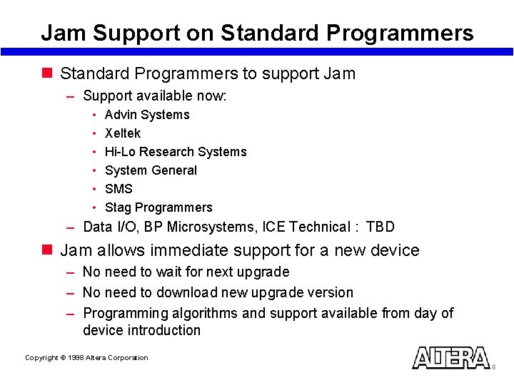
Jam Support on Standard Programmers to support Jam – Support available now: • • • Advin Systems Xeltek Hi-Lo Research Systems System General SMS Stag Programmers – Data I/O, BP Microsystems, ICE Technical : TBD n Jam allows immediate support for a new device – No need to wait for next upgrade – No need to download new upgrade version – Programming algorithms and support available from day of device introduction Copyright © 1998 Altera Corporation

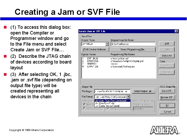
Creating a Jam or SVF File n (1) To access this dialog box: open the Compiler or Programmer window and go to the File menu and select Create Jam or SVF File… n (2) Describe the JTAG chain of devices according to board layout n (3) After selecting OK, 1. jbc, . jam or. svf file (depending on output file type) will be created representing all devices in the chain Copyright © 1998 Altera Corporation

Updating a Jam File n With a given. pof file, different (newer) devices can be programmed using the same file – I. e. a given. pof file generated for a MAX 7000 S device can be used to program its MAX 7000 A counterpart – The system (I. e. the latest version of MAX+plus II) looks up the silicon ID of the device, chooses the algorithm, and programs the device n To program a newer device with Jam, the Jam file (. jam or. jbc) must be updated to include the algorithm for the newer device – Use the version of MAX+plus II that supports the newer device to re-generate the Jam file from the older. pof file – Re-compiling the design is NOT necessary Copyright © 1998 Altera Corporation

SVF 2 Jam n SVF 2 Jam conversion utility is available from http: //www. jamisp. com n This utility demonstrates the truly vendorindependence of the Jam language n SVF 2 Jam does a literal translation of each SVF statement to the corresponding Jam statement – For an optimized Jam file, use the device vendor’s Jam Composer Copyright © 1998 Altera Corporation

Using Download Cables Copyright © 1998 Altera Corporation

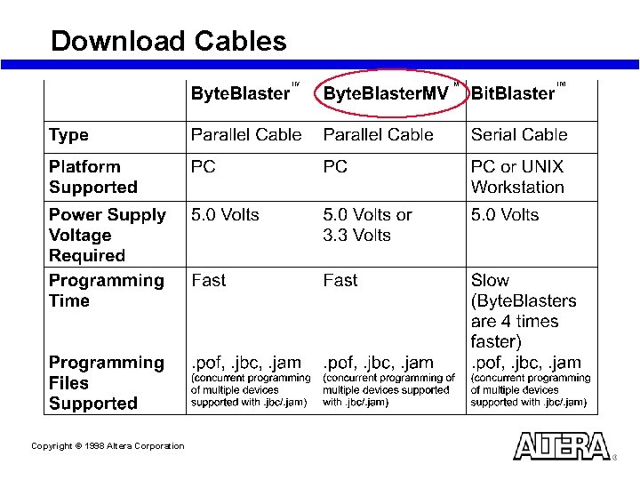
Why Use a Download Cable? n A download cable channels programming data between a PC or UNIX workstation and the circuit board n Design changes downloaded directly to devices – Easy prototyping – Multiple design iterations accomplished quickly Copyright © 1998 Altera Corporation

Download Cables Copyright © 1998 Altera Corporation

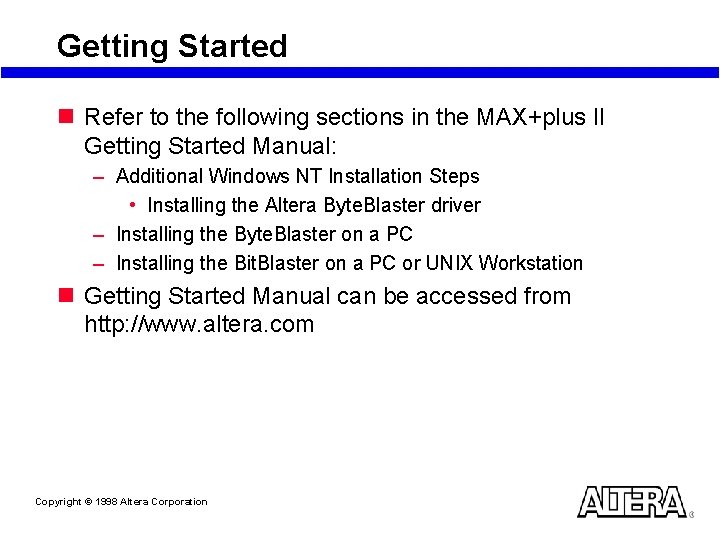
Getting Started n Refer to the following sections in the MAX+plus II Getting Started Manual: – Additional Windows NT Installation Steps • Installing the Altera Byte. Blaster driver – Installing the Byte. Blaster on a PC – Installing the Bit. Blaster on a PC or UNIX Workstation n Getting Started Manual can be accessed from http: //www. altera. com Copyright © 1998 Altera Corporation

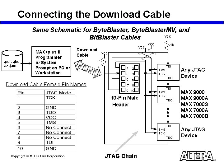
Connecting the Download Cable Same Schematic for Byte. Blaster, Byte. Blaster. MV, and VCC Bit. Blaster Cables . pof, . jbc or. jam MAX+plus II Programmer or System Prompt on PC or Workstation Download Cable Female Pin Names VCC 1 k 1 k 1 k 1 2 3 4 5 6 7 8 9 10 10 -Pin Male Header TDI TMS TCK TDO Copyright © 1998 Altera Corporation JTAG Chain Any JTAG Device MAX 9000 A MAX 7000 S MAX 7000 A MAX 7000 B Any JTAG Device

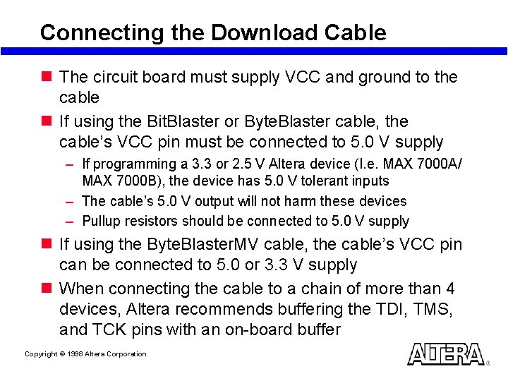
Connecting the Download Cable n The circuit board must supply VCC and ground to the cable n If using the Bit. Blaster or Byte. Blaster cable, the cable’s VCC pin must be connected to 5. 0 V supply – If programming a 3. 3 or 2. 5 V Altera device (I. e. MAX 7000 A/ MAX 7000 B), the device has 5. 0 V tolerant inputs – The cable’s 5. 0 V output will not harm these devices – Pullup resistors should be connected to 5. 0 V supply n If using the Byte. Blaster. MV cable, the cable’s VCC pin can be connected to 5. 0 or 3. 3 V supply n When connecting the cable to a chain of more than 4 devices, Altera recommends buffering the TDI, TMS, and TCK pins with an on-board buffer Copyright © 1998 Altera Corporation

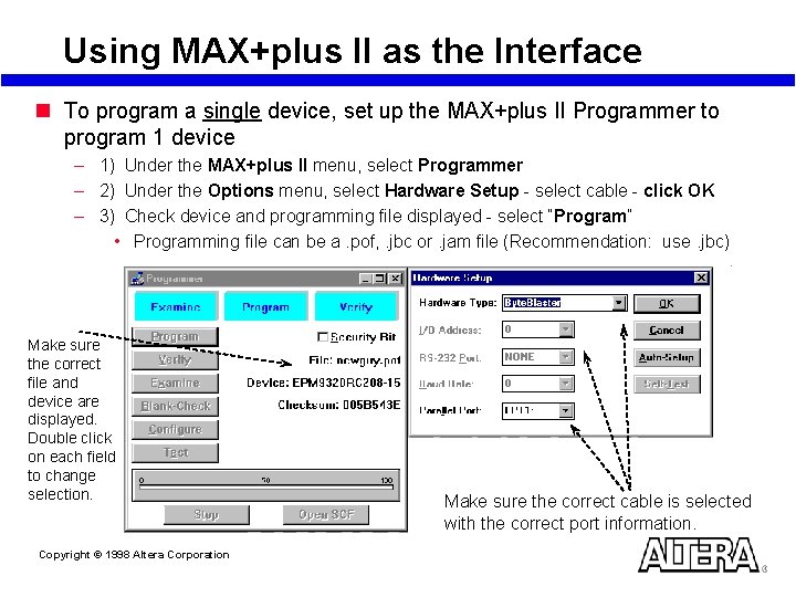
Using MAX+plus II as the Interface n To program a single device, set up the MAX+plus II Programmer to program 1 device – 1) Under the MAX+plus II menu, select Programmer – 2) Under the Options menu, select Hardware Setup - select cable - click OK – 3) Check device and programming file displayed - select “Program” • Programming file can be a. pof, . jbc or. jam file (Recommendation: use. jbc) Make sure the correct file and device are displayed. Double click on each field to change selection. Copyright © 1998 Altera Corporation Make sure the correct cable is selected with the correct port information.

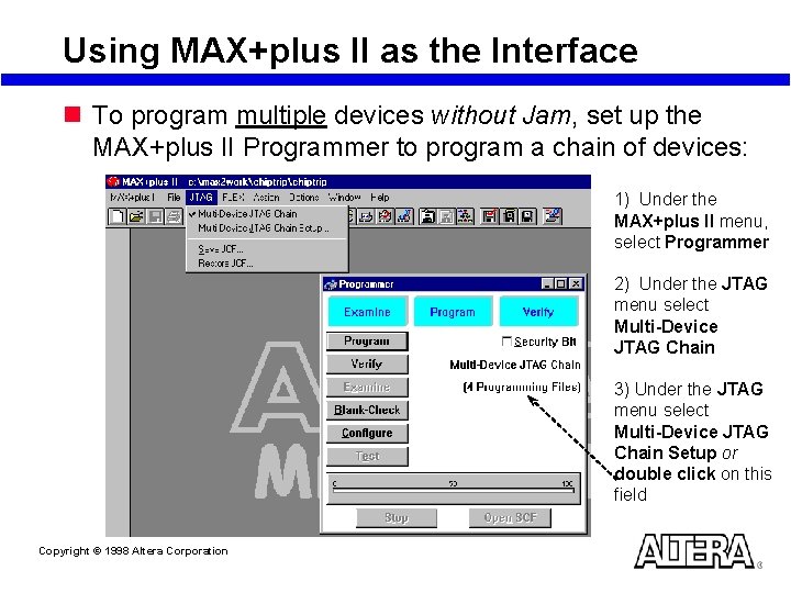
Using MAX+plus II as the Interface n To program multiple devices without Jam, set up the MAX+plus II Programmer to program a chain of devices: 1) Under the MAX+plus II menu, select Programmer 2) Under the JTAG menu select Multi-Device JTAG Chain 3) Under the JTAG menu select Multi-Device JTAG Chain Setup or double click on this field Copyright © 1998 Altera Corporation

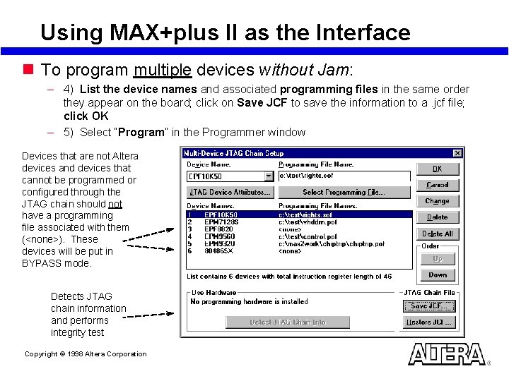
Using MAX+plus II as the Interface n To program multiple devices without Jam: – 4) List the device names and associated programming files in the same order they appear on the board; click on Save JCF to save the information to a. jcf file; click OK – 5) Select “Program” in the Programmer window Devices that are not Altera devices and devices that cannot be programmed or configured through the JTAG chain should not have a programming file associated with them (<none>). These devices will be put in BYPASS mode. Detects JTAG chain information and performs integrity test Copyright © 1998 Altera Corporation

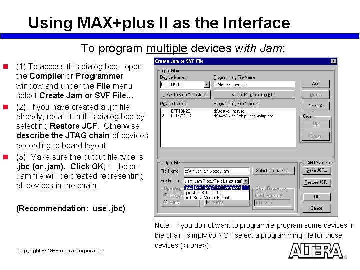
Using MAX+plus II as the Interface To program multiple devices with Jam: n (1) To access this dialog box: open the Compiler or Programmer window and under the File menu select Create Jam or SVF File… n (2) If you have created a. jcf file already, recall it in this dialog box by selecting Restore JCF. Otherwise, describe the JTAG chain of devices according to board layout. n (3) Make sure the output file type is. jbc (or. jam). Click OK; 1. jbc or. jam file will be created representing all devices in the chain. (Recommendation: use. jbc) Copyright © 1998 Altera Corporation Note: If you do not want to program/re-program some devices in the chain, simply do NOT select a programming file for those devices (<none>)

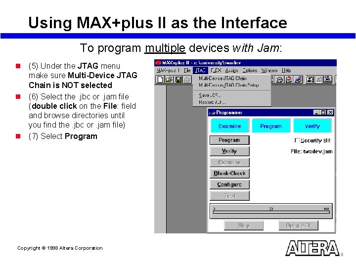
Using MAX+plus II as the Interface To program multiple devices with Jam: n (5) Under the JTAG menu make sure Multi-Device JTAG Chain is NOT selected n (6) Select the. jbc or. jam file (double click on the File: field and browse directories until you find the. jbc or. jam file) n (7) Select Program Copyright © 1998 Altera Corporation

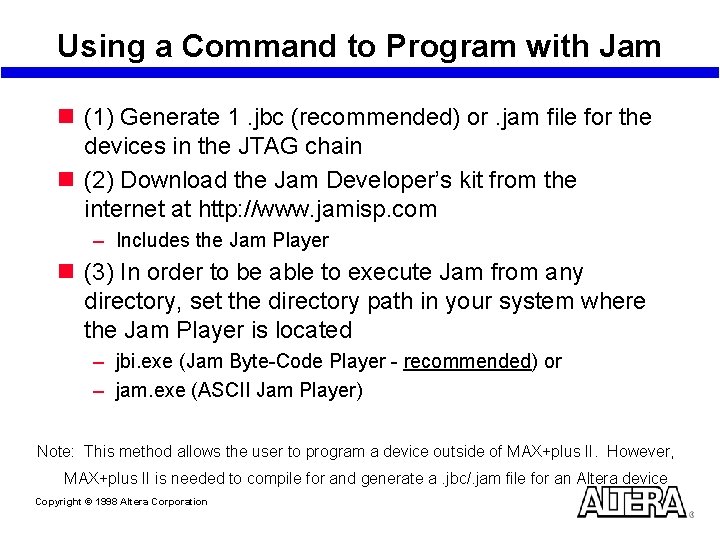
Using a Command to Program with Jam n (1) Generate 1. jbc (recommended) or. jam file for the devices in the JTAG chain n (2) Download the Jam Developer’s kit from the internet at http: //www. jamisp. com – Includes the Jam Player n (3) In order to be able to execute Jam from any directory, set the directory path in your system where the Jam Player is located – jbi. exe (Jam Byte-Code Player - recommended) or – jam. exe (ASCII Jam Player) Note: This method allows the user to program a device outside of MAX+plus II. However, MAX+plus II is needed to compile for and generate a. jbc/. jam file for an Altera device Copyright © 1998 Altera Corporation
![Executing the Jam Player n jbi or jam h v d varval p port Executing the Jam Player n jbi or jam [-h] [-v] [-d <var=val>] [-p <port>]](https://slidetodoc.com/presentation_image/34aa1f691e49440f467bcaf796d6e3e1/image-145.jpg)
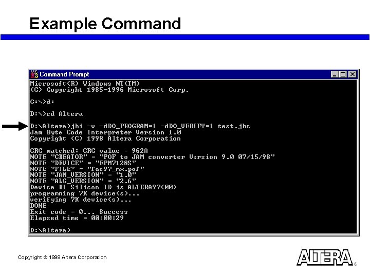
Executing the Jam Player n jbi or jam [-h] [-v] [-d <var=val>] [-p <port>] [-s <port>] [-m <mem>] <filename> – -h Help message – -v Verbose messages – -d Initialize variable to specified value • See next slide for variables and values – -p Parallel port number or address (for Byte. Blaster) – -s Serial port name (for Bit. Blaster) – -m Fixed memory buffer size in bytes • By default, memory is allocated dynamically – <filename> is the file (I. e. filename. jbc) n Suggestion: type jbi -h to get the above definitions and ensure the system recognizes the Jam Player Copyright © 1998 Altera Corporation
![Executing the Jam Player n jbi or jam h v d varval p port Executing the Jam Player n jbi or jam [-h] [-v] [-d <var=val>] [-p <port>]](https://slidetodoc.com/presentation_image/34aa1f691e49440f467bcaf796d6e3e1/image-146.jpg)
Executing the Jam Player n jbi or jam [-h] [-v] [-d <var=val>] [-p <port>] [-s <port>] [-m <mem>] <filename> n -d Variables and values – DO_VERIFY – DO_ERASE • 0 • 1 Do not perform a bulk erase Perform a bulk erase – DO_BLANKCHECK • 0 • 1 Do not check the erased state of the device Check the erased state of the device – DO_PROGRAM • 0 • 1 Do not program the device Program the device • 0 • 1 – DO_READ_UES • 0 • 1 Do not read the JTAG UES code Read and report the UES code – DO_SECURE • 0 • 1 Do not set the security bit Set the security bit if the corresponding. pof sets the security bit – DO_SECURE_ALL • 0 • 1 Copyright © 1998 Altera Corporation Do not verify the device Verify the device Do not set the security bit Set the security bit overriding. pof settings

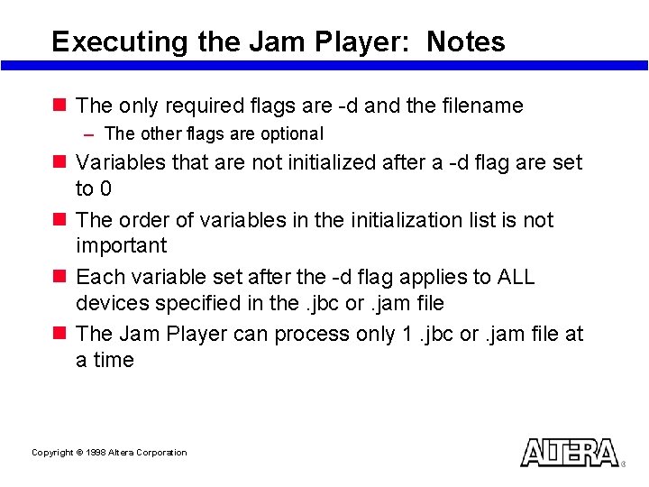
Executing the Jam Player: Notes n The only required flags are -d and the filename – The other flags are optional n Variables that are not initialized after a -d flag are set to 0 n The order of variables in the initialization list is not important n Each variable set after the -d flag applies to ALL devices specified in the. jbc or. jam file n The Jam Player can process only 1. jbc or. jam file at a time Copyright © 1998 Altera Corporation

Example Command Copyright © 1998 Altera Corporation

Laboratory Exercise 4 Go to Laboratory Exercise Manual and Complete Exercise 4 Copyright © 1998 Altera Corporation

Using In-Circuit Testers Copyright © 1998 Altera Corporation

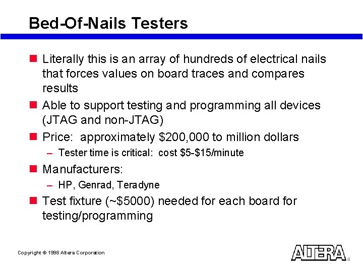
Bed-Of-Nails Testers n Literally this is an array of hundreds of electrical nails that forces values on board traces and compares results n Able to support testing and programming all devices (JTAG and non-JTAG) n Price: approximately $200, 000 to million dollars – Tester time is critical: cost $5 -$15/minute n Manufacturers: – HP, Genrad, Teradyne n Test fixture (~$5000) needed for each board for testing/programming Copyright © 1998 Altera Corporation

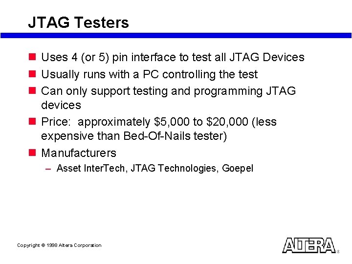
JTAG Testers n Uses 4 (or 5) pin interface to test all JTAG Devices n Usually runs with a PC controlling the test n Can only support testing and programming JTAG devices n Price: approximately $5, 000 to $20, 000 (less expensive than Bed-Of-Nails tester) n Manufacturers – Asset Inter. Tech, JTAG Technologies, Goepel Copyright © 1998 Altera Corporation

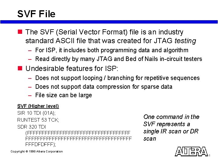
SVF File n The SVF (Serial Vector Format) file is an industry standard ASCII file that was created for JTAG testing – For ISP, it includes both programming data and algorithm – Read directly by many JTAG and Bed of Nails in-circuit testers n Undesirable features for ISP: – Does not support looping / branching for repetitive sequences – Does not support data compression for sparse data – File size can be large SVF (Higher level) SIR 10 TDI (01 A); RUNTEST 53 TCK; SDR 320 TDI (FFFFFFFFFFFFFFFFFFFFFFFFFFFFFFFFFFF FFFDFDFFF); Copyright © 1998 Altera Corporation One command in the SVF represents a single IR scan or DR scan

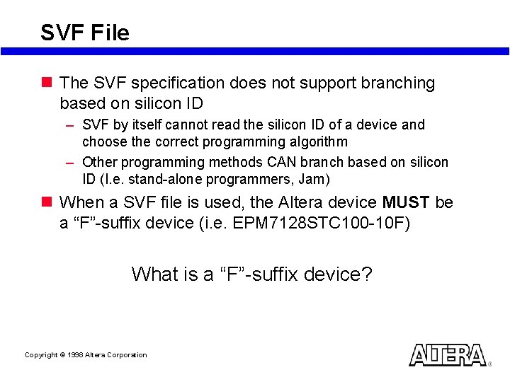
SVF File n The SVF specification does not support branching based on silicon ID – SVF by itself cannot read the silicon ID of a device and choose the correct programming algorithm – Other programming methods CAN branch based on silicon ID (I. e. stand-alone programmers, Jam) n When a SVF file is used, the Altera device MUST be a “F”-suffix device (i. e. EPM 7128 STC 100 -10 F) What is a “F”-suffix device? Copyright © 1998 Altera Corporation

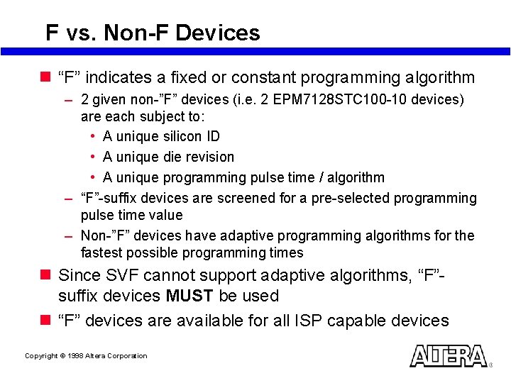
F vs. Non-F Devices n “F” indicates a fixed or constant programming algorithm – 2 given non-”F” devices (i. e. 2 EPM 7128 STC 100 -10 devices) are each subject to: • A unique silicon ID • A unique die revision • A unique programming pulse time / algorithm – “F”-suffix devices are screened for a pre-selected programming pulse time value – Non-”F” devices have adaptive programming algorithms for the fastest possible programming times n Since SVF cannot support adaptive algorithms, “F”suffix devices MUST be used n “F” devices are available for all ISP capable devices Copyright © 1998 Altera Corporation

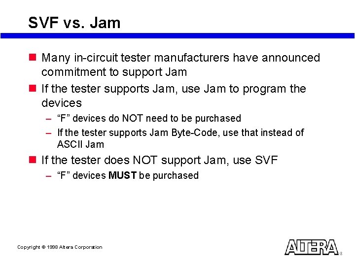
SVF vs. Jam n Many in-circuit tester manufacturers have announced commitment to support Jam n If the tester supports Jam, use Jam to program the devices – “F” devices do NOT need to be purchased – If the tester supports Jam Byte-Code, use that instead of ASCII Jam n If the tester does NOT support Jam, use SVF – “F” devices MUST be purchased Copyright © 1998 Altera Corporation

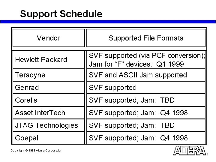
Support Schedule Vendor Supported File Formats Hewlett Packard SVF supported (via PCF conversion); Jam for “F” devices: Q 1 1999 Teradyne SVF and ASCII Jam supported Genrad SVF supported Corelis SVF supported; Jam: TBD Asset Inter. Tech SVF supported; Jam: Q 4 1998 JTAG Technologies SVF supported; Jam: TBD Goepel SVF supported; Jam: Q 4 1998 Copyright © 1998 Altera Corporation

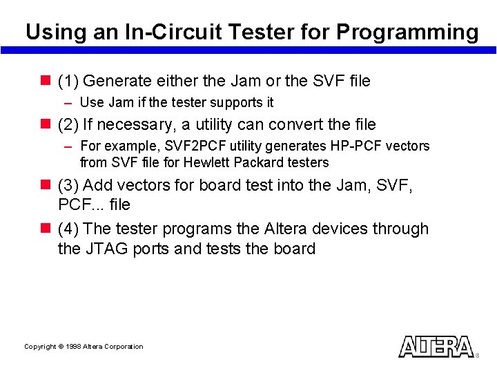
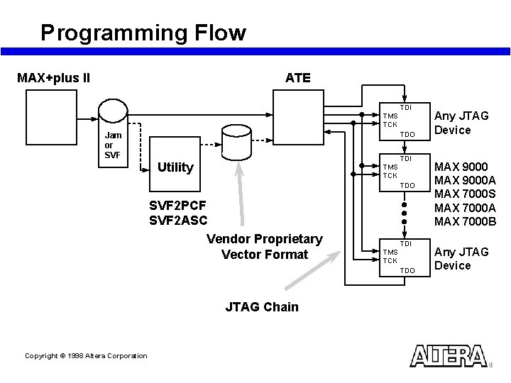
Using an In-Circuit Tester for Programming n (1) Generate either the Jam or the SVF file – Use Jam if the tester supports it n (2) If necessary, a utility can convert the file – For example, SVF 2 PCF utility generates HP-PCF vectors from SVF file for Hewlett Packard testers n (3) Add vectors for board test into the Jam, SVF, PCF. . . file n (4) The tester programs the Altera devices through the JTAG ports and tests the board Copyright © 1998 Altera Corporation

Programming Flow ATE MAX+plus II TDI TMS TCK Jam or SVF TDO TDI Utility TMS TCK TDO SVF 2 PCF SVF 2 ASC Vendor Proprietary Vector Format TDI TMS TCK TDO JTAG Chain Copyright © 1998 Altera Corporation Any JTAG Device MAX 9000 A MAX 7000 S MAX 7000 A MAX 7000 B Any JTAG Device

Using an Embedded Processor Copyright © 1998 Altera Corporation

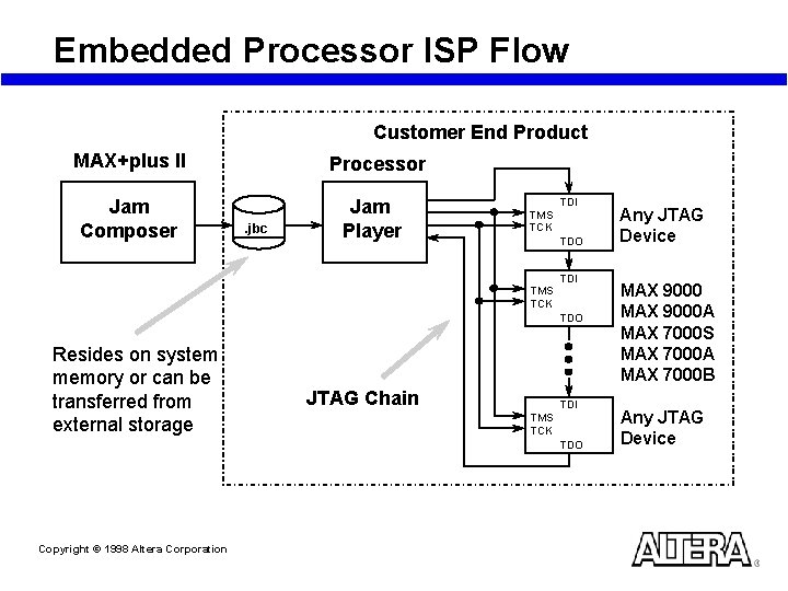
Embedded Processor ISP Flow Customer End Product MAX+plus II Processor Jam Composer Jam Player . jbc TDI TMS TCK TDO Resides on system memory or can be transferred from external storage JTAG Chain TDI TMS TCK TDO Copyright © 1998 Altera Corporation Any JTAG Device MAX 9000 A MAX 7000 S MAX 7000 A MAX 7000 B Any JTAG Device

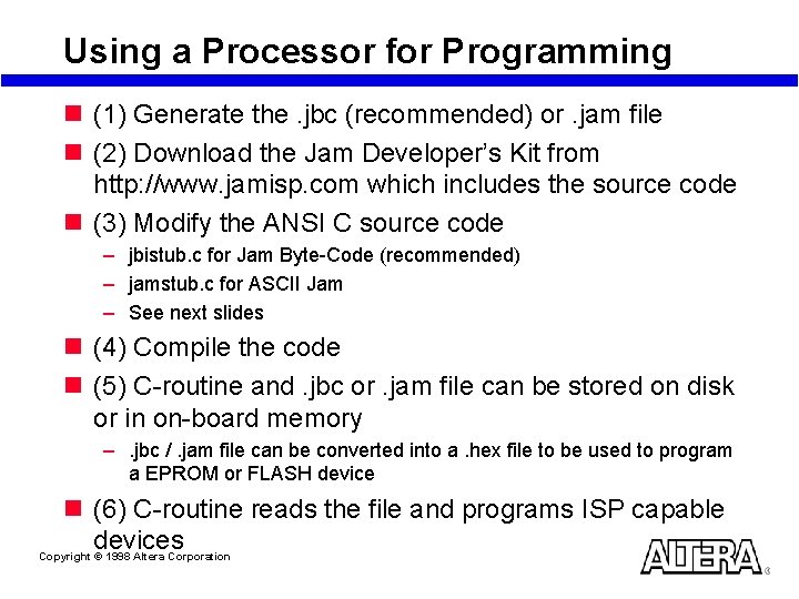
Using a Processor for Programming n (1) Generate the. jbc (recommended) or. jam file n (2) Download the Jam Developer’s Kit from http: //www. jamisp. com which includes the source code n (3) Modify the ANSI C source code – jbistub. c for Jam Byte-Code (recommended) – jamstub. c for ASCII Jam – See next slides n (4) Compile the code n (5) C-routine and. jbc or. jam file can be stored on disk or in on-board memory –. jbc /. jam file can be converted into a. hex file to be used to program a EPROM or FLASH device n (6) C-routine reads the file and programs ISP capable devices Copyright © 1998 Altera Corporation

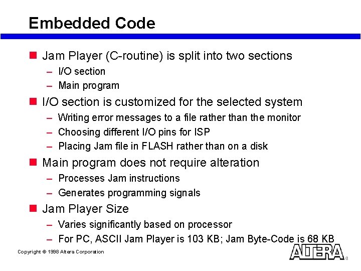
Embedded Code n Jam Player (C-routine) is split into two sections – I/O section – Main program n I/O section is customized for the selected system – Writing error messages to a file rather than the monitor – Choosing different I/O pins for ISP – Placing Jam file in FLASH rather than on a disk n Main program does not require alteration – Processes Jam instructions – Generates programming signals n Jam Player Size – Varies significantly based on processor – For PC, ASCII Jam Player is 103 KB; Jam Byte-Code is 68 KB Copyright © 1998 Altera Corporation

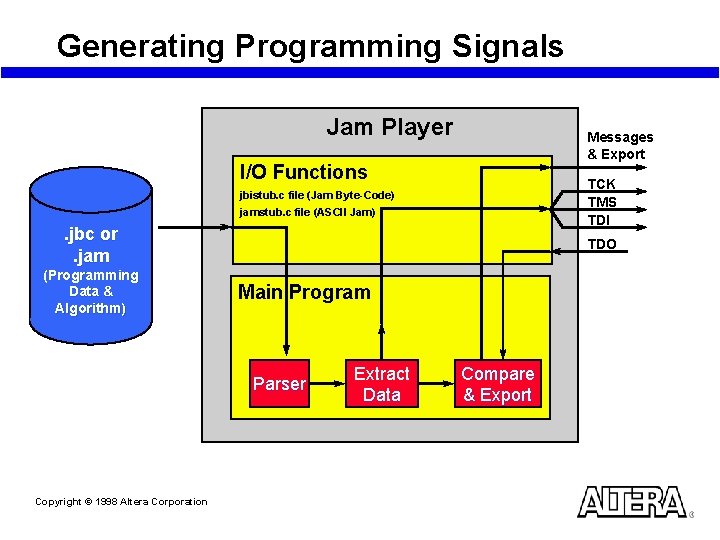
Generating Programming Signals Jam Player Messages & Export I/O Functions TCK TMS TDI jbistub. c file (Jam Byte-Code) jamstub. c file (ASCII Jam) . jbc or. jam (Programming Data & Algorithm) TDO Main Program Parser Copyright © 1998 Altera Corporation Extract Data Compare & Export

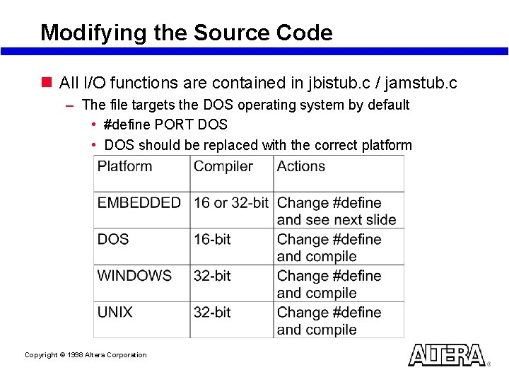
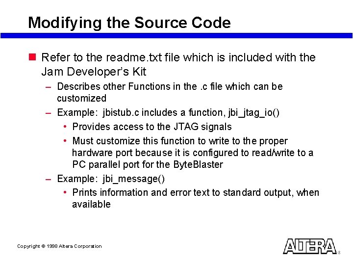
Modifying the Source Code n All I/O functions are contained in jbistub. c / jamstub. c – The file targets the DOS operating system by default • #define PORT DOS • DOS should be replaced with the correct platform Copyright © 1998 Altera Corporation

Modifying the Source Code n Refer to the readme. txt file which is included with the Jam Developer’s Kit – Describes other Functions in the. c file which can be customized – Example: jbistub. c includes a function, jbi_jtag_io() • Provides access to the JTAG signals • Must customize this function to write to the proper hardware port because it is configured to read/write to a PC parallel port for the Byte. Blaster – Example: jbi_message() • Prints information and error text to standard output, when available Copyright © 1998 Altera Corporation

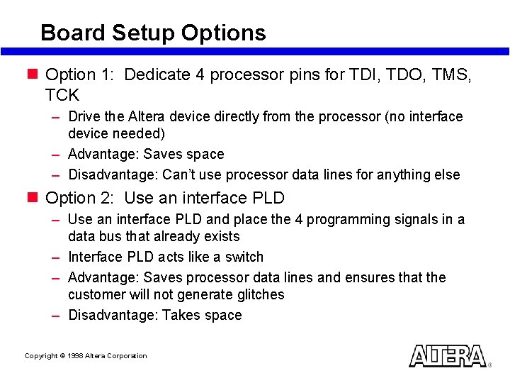
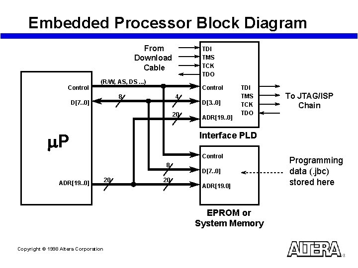
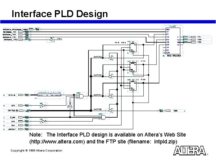
Board Setup Options n Option 1: Dedicate 4 processor pins for TDI, TDO, TMS, TCK – Drive the Altera device directly from the processor (no interface device needed) – Advantage: Saves space – Disadvantage: Can’t use processor data lines for anything else n Option 2: Use an interface PLD – Use an interface PLD and place the 4 programming signals in a data bus that already exists – Interface PLD acts like a switch – Advantage: Saves processor data lines and ensures that the customer will not generate glitches – Disadvantage: Takes space Copyright © 1998 Altera Corporation

Embedded Processor Block Diagram From Download Cable Control TDI TMS TCK TDO (R/W, AS, DS. . . ) Control 4 8 D[7. . 0] 20 m. P D[3. . 0] ADR[19. . 0] TDI TMS TCK TDO Interface PLD Control 8 ADR[19. . 0] 20 20 D[7. . 0] ADR[19. 0] EPROM or System Memory Copyright © 1998 Altera Corporation To JTAG/ISP Chain Programming data (. jbc) stored here

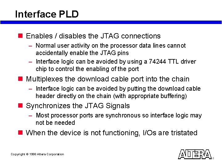
Interface PLD n Enables / disables the JTAG connections – Normal user activity on the processor data lines cannot accidentally enable the JTAG pins – Interface logic can be avoided by using a 74244 TTL driver chip to control the enabling of the port n Multiplexes the download cable port into the chain – Interface logic can be avoided by putting the download cable header directly on the chain (with appropriate buffering) n Synchronizes the JTAG Signals – Most processor ports are synchronous so interface logic may not be needed n When the device is not functioning, I/Os are tristated Copyright © 1998 Altera Corporation

Interface PLD Design Note: The Interface PLD design is available on Altera’s Web Site (http: //www. altera. com) and the FTP site (filename: intpld. zip) Copyright © 1998 Altera Corporation

Debugging Tips n Add a Byte. Blaster header for prototype stage (debugging) – If the processor is unable to program the device, using the download cable will help determine the cause: • Error in customization of code • Problem with hardware: devices or board n Byte. Blaster and MAX+plus II can be used to detect the JTAG chain n Once ISP is successful with the embedded processor, this 10 -pin header does not need to assembled Copyright © 1998 Altera Corporation

8051 Processor n Popular 8 -bit microprocessor – Supports 1 MHz - 50 MHz clock frequencies n Standard Jam Players only support 16 and 32 -bit processors n 8051 -specific Jam Byte-Code Player developed n Programming times much longer – 10 -15 minutes to program EPM 7064 S (with f. CLK = 12 MHz) – Use fastest 8051 variant for shortest programming times n Requires data compression to support large devices – EPM 7256 S or larger devices – Chain of devices Copyright © 1998 Altera Corporation

In-System Programming Times Copyright © 1998 Altera Corporation

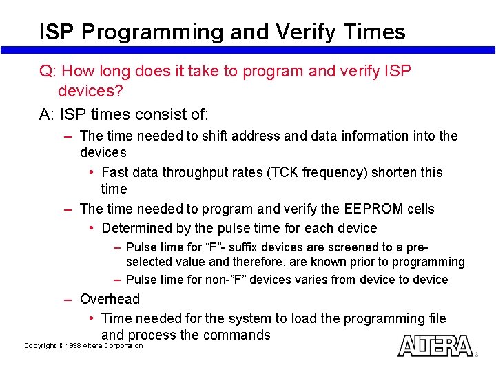
ISP Programming and Verify Times Q: How long does it take to program and verify ISP devices? A: ISP times consist of: – The time needed to shift address and data information into the devices • Fast data throughput rates (TCK frequency) shorten this time – The time needed to program and verify the EEPROM cells • Determined by the pulse time for each device – Pulse time for “F”- suffix devices are screened to a preselected value and therefore, are known prior to programming – Pulse time for non-”F” devices varies from device to device – Overhead • Time needed for the system to load the programming file and process the commands Copyright © 1998 Altera Corporation

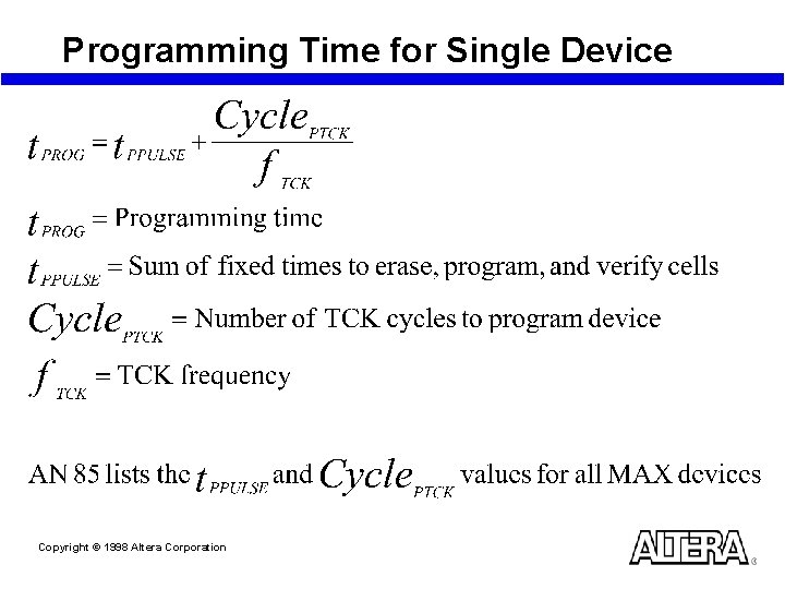
Programming Time for Single Device Copyright © 1998 Altera Corporation

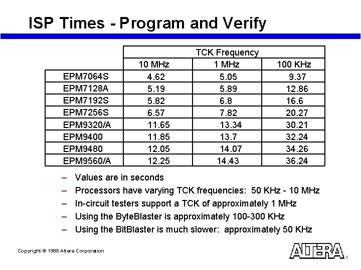
ISP Times - Program and Verify EPM 7064 S EPM 7128 A EPM 7192 S EPM 7256 S EPM 9320/A EPM 9400 EPM 9480 EPM 9560/A – – – 10 MHz 4. 62 5. 19 5. 82 6. 57 11. 65 11. 85 12. 05 12. 25 TCK Frequency 1 MHz 5. 05 5. 89 6. 8 7. 82 13. 34 13. 7 14. 07 14. 43 100 KHz 9. 37 12. 86 16. 6 20. 27 30. 21 32. 24 34. 26 36. 24 Values are in seconds Processors have varying TCK frequencies: 50 KHz - 10 MHz In-circuit testers support a TCK of approximately 1 MHz Using the Byte. Blaster is approximately 100 -300 KHz Using the Bit. Blaster is much slower: approximately 50 KHz Copyright © 1998 Altera Corporation

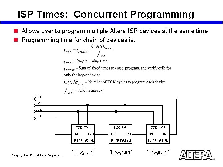
ISP Times: Concurrent Programming n Allows user to program multiple Altera ISP devices at the same time n Programming time for chain of devices is: TDO TMS TCK TDI TCK TMS TDI Copyright © 1998 Altera Corporation TDO TCK TMS TDI TDO EPM 9560 EPM 9320 EPM 9400 “Program”

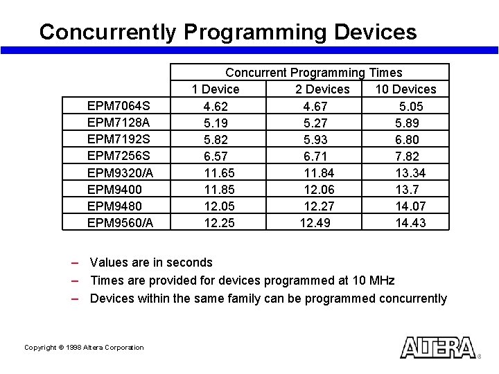
Concurrently Programming Devices EPM 7064 S EPM 7128 A EPM 7192 S EPM 7256 S EPM 9320/A EPM 9400 EPM 9480 EPM 9560/A Concurrent Programming Times 2 Devices 10 Devices 1 Device 4. 62 4. 67 5. 05 5. 19 5. 27 5. 89 5. 82 5. 93 6. 80 6. 57 6. 71 7. 82 11. 84 13. 34 11. 65 12. 06 13. 7 11. 85 12. 27 14. 07 12. 05 12. 49 14. 43 12. 25 – Values are in seconds – Times are provided for devices programmed at 10 MHz – Devices within the same family can be programmed concurrently Copyright © 1998 Altera Corporation

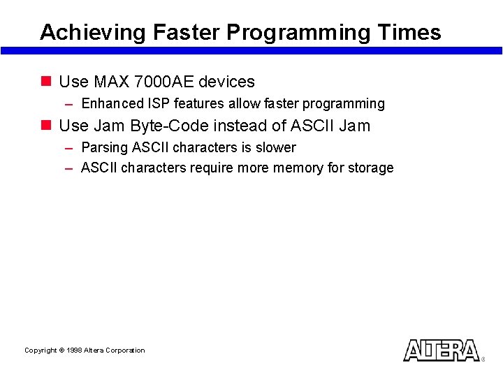
Achieving Faster Programming Times n Use MAX 7000 AE devices – Enhanced ISP features allow faster programming n Use Jam Byte-Code instead of ASCII Jam – Parsing ASCII characters is slower – ASCII characters require more memory for storage Copyright © 1998 Altera Corporation

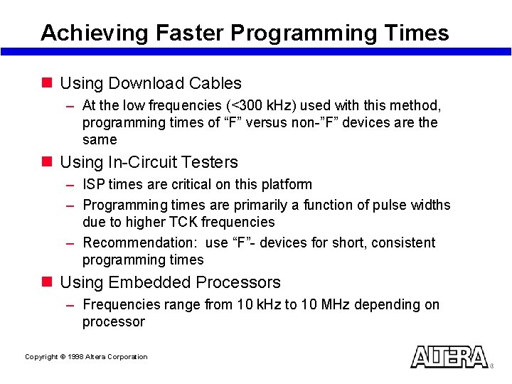
Achieving Faster Programming Times n Using Download Cables – At the low frequencies (<300 k. Hz) used with this method, programming times of “F” versus non-”F” devices are the same n Using In-Circuit Testers – ISP times are critical on this platform – Programming times are primarily a function of pulse widths due to higher TCK frequencies – Recommendation: use “F”- devices for short, consistent programming times n Using Embedded Processors – Frequencies range from 10 k. Hz to 10 MHz depending on processor Copyright © 1998 Altera Corporation

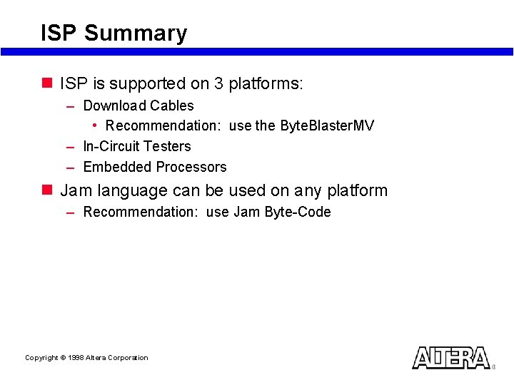
ISP Summary n ISP is supported on 3 platforms: – Download Cables • Recommendation: use the Byte. Blaster. MV – In-Circuit Testers – Embedded Processors n Jam language can be used on any platform – Recommendation: use Jam Byte-Code Copyright © 1998 Altera Corporation

References n n n n MAX 9000 Programmable Logic Device Family Data Sheet MAX 7000 A Programmable Logic Device Family Data Sheet Operating Requirements for Altera Devices Data Sheet AN 31: Fitting Designs in MAX 7000 EPLDs AN 43: Designing with MAX 9000 Devices AN 77: Understanding MAX 9000 Timing AN 94: Understanding MAX 7000 Timing Latest document versions available from www. altera. com Copyright © 1998 Altera Corporation

Referenced (continued) n n n AN 74: Evaluating Power for Altera Devices AN 75: High-Speed Board Designs Programming Hardware Manufacturers In-Circuit Test Vendor Support Third-Party Programmer Support for the Jam Language n Bit. Blaster Serial Download Cable Data Sheet n Byte. Blaster Parallel Port Download Cable Data Sheet n Byte. Blaster. MV Parallel Port Download Cable Data Sheet Latest document versions available from www. altera. com Copyright © 1998 Altera Corporation

References (continued) n AN 39: JTAG Boundary-Scan Testing in Altera Devices n AN 85: ISP Programming Times for MAX 7000 and MAX 9000 Devices n AN 88: Using the Jam Language for ISP via an Embedded Processor n AN 95: In-System Programmability in MAX Devices n AN 100: In-System Programmability Guidelines n ISP CDROM (contains most of the above documents) n ISP Handbook (contains most of the above documents) n http: //www. jamisp. com (includes Developer’s Kit with Jam Language Specification) Latest document versions available from www. altera. com Copyright © 1998 Altera Corporation

Altera Technical Support n Reference the MAX+plus II on-line help n World-wide web: http: //www. altera. com – Latest literature (Application Notes, Data Sheets…) – Use ATLAS (Altera Technical Support) solutions to search for answers to technical problems – Customer training class schedule & registration n Consult Altera Applications – Factory Applications Engineers: Hotline: (800) 800 -EPLD (6: 00 a. m. - 6: 00 p. m. PST) or E-mail: sos@altera. com – Field Applications Engineers: Contact your local Altera sales office n FTP: ftp. altera. com n Literature via mail: 1 -888 -3 -ALTERA Copyright © 1998 Altera Corporation