Optimization of planar pixel detector T Habermann Planar
Optimization of planar pixel detector T. Habermann
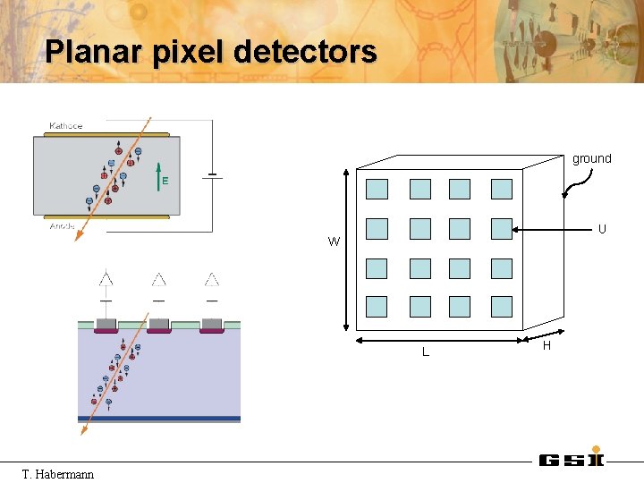
Planar pixel detectors ground U W L T. Habermann H
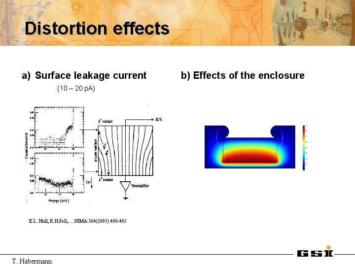
Distortion effects a) Surface leakage current (10 – 20 p. A) E. L. Hull, R. H. Pell, …NIMA 364(1995) 488 -495 T. Habermann b) Effects of the enclosure
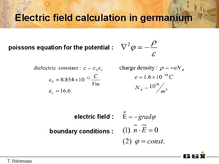
Electric field calculation in germanium poissons equation for the potential : electric field : boundary conditions : T. Habermann
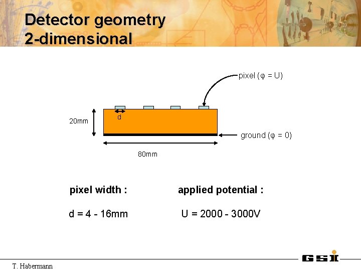
Detector geometry 2 -dimensional pixel (φ = U) 20 mm d ground (φ = 0) 80 mm T. Habermann pixel width : applied potential : d = 4 - 16 mm U = 2000 - 3000 V
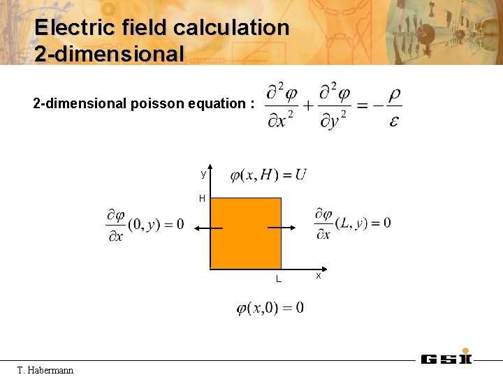
Electric field calculation 2 -dimensional poisson equation : y H L T. Habermann x

Finite-Volume-Method The region is divided into N rectangular controlvolumes (CV). The potential is approximated in the center of this CV’s → 2 -d grid For every CV we get an equation of the form : a. PΦP - awΦW - a. NΦN - a. EΦE - a. SΦS = b. P → 3 -d grid linear system of equations with N variables : AΦ=b T. Habermann (“Computational Methods for Fluid Dynamics”, J. H. Ferziger, M. Peric)
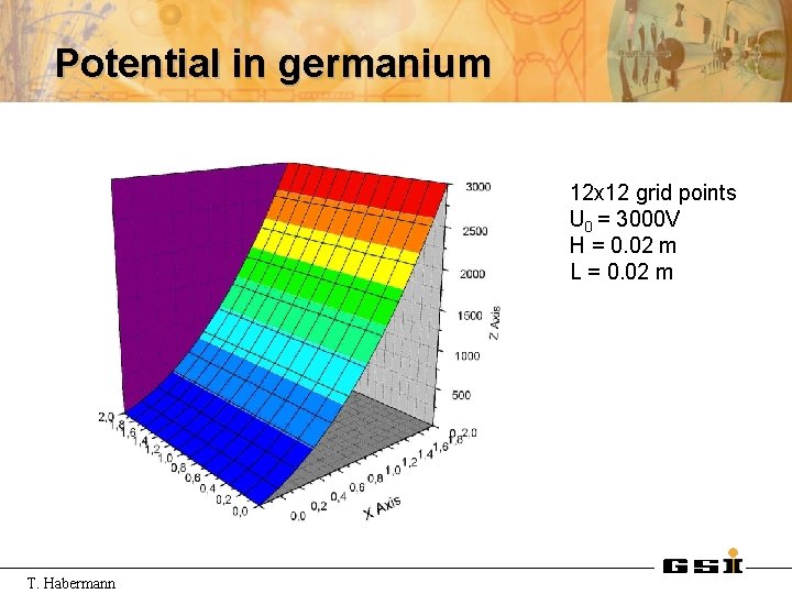
Potential in germanium 12 x 12 grid points U 0 = 3000 V H = 0. 02 m L = 0. 02 m T. Habermann
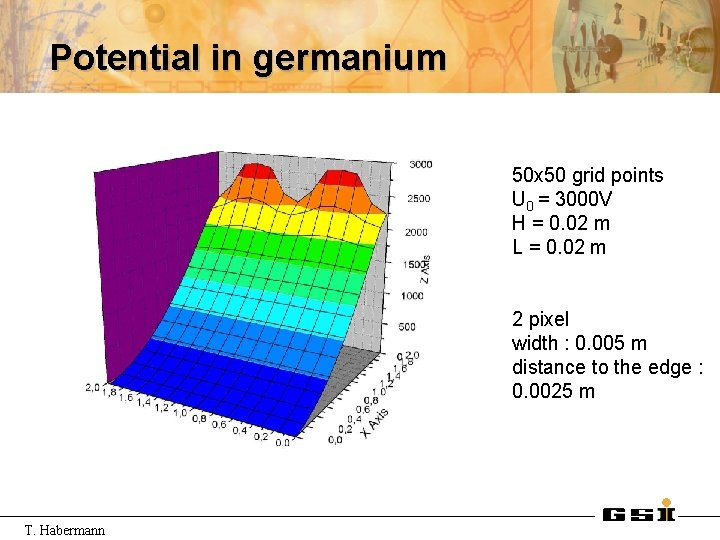
Potential in germanium 50 x 50 grid points U 0 = 3000 V H = 0. 02 m L = 0. 02 m 2 pixel width : 0. 005 m distance to the edge : 0. 0025 m T. Habermann
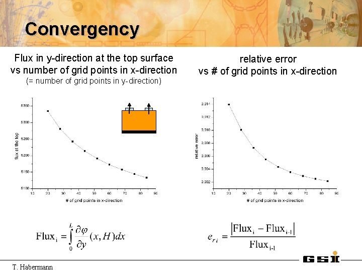
Convergency Flux in y-direction at the top surface vs number of grid points in x-direction (= number of grid points in y-direction) T. Habermann relative error vs # of grid points in x-direction

outlook • further examination of convergency behaviour (→ adjustment of the numerical method for better convergency) • 3 d model • examination of the electric field and reconstruction of the expected effects : • distortion caused by the enclosure • distortion caused by surface leakage current • How do the free parameters influence these effects ? (distance between pixels, pixelsize, size of the capsule, . . . ) • GOAL : Minimize the electric field distortion by choosing the right parameter values T. Habermann
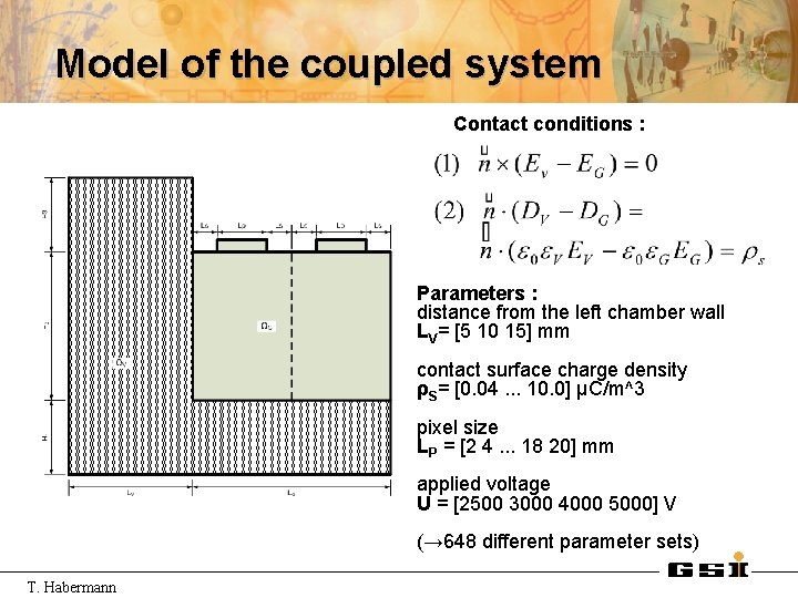
Model of the coupled system Contact conditions : Parameters : distance from the left chamber wall LV= [5 10 15] mm contact surface charge density ρS= [0. 04. . . 10. 0] μC/m^3 pixel size LP = [2 4. . . 18 20] mm applied voltage U = [2500 3000 4000 5000] V (→ 648 different parameter sets) T. Habermann
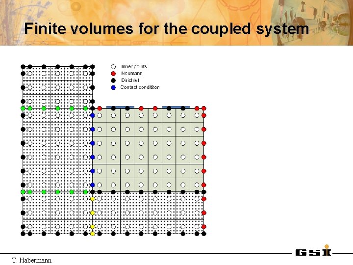
Finite volumes for the coupled system T. Habermann
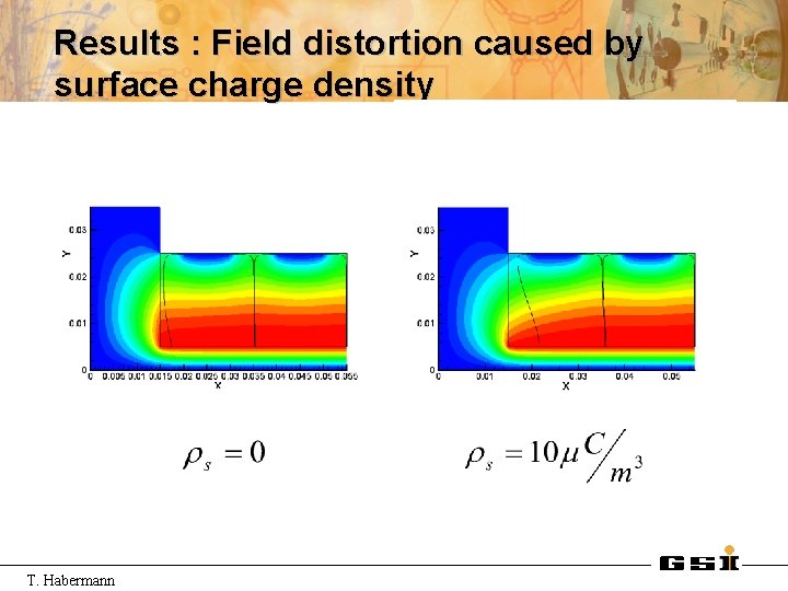
Results : Field distortion caused by surface charge density T. Habermann
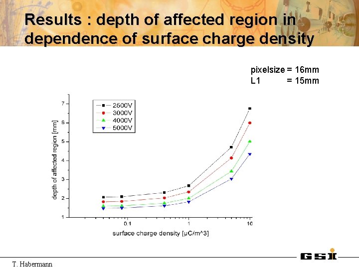
Results : depth of affected region in dependence of surface charge density pixelsize = 16 mm L 1 = 15 mm T. Habermann
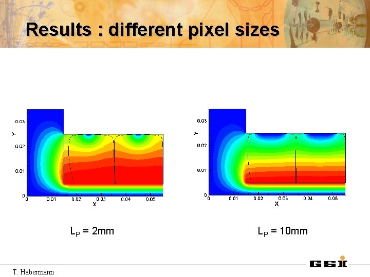
Results : different pixel sizes LP = 2 mm T. Habermann LP = 10 mm
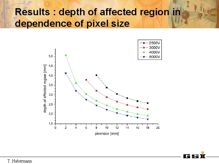
Results : depth of affected region in dependence of pixel size T. Habermann
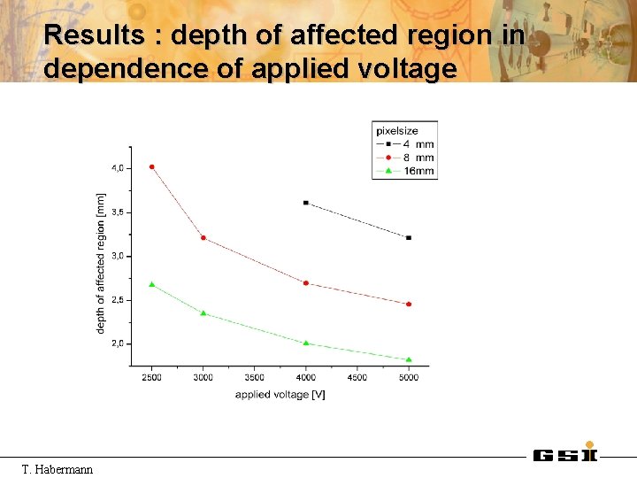
Results : depth of affected region in dependence of applied voltage T. Habermann
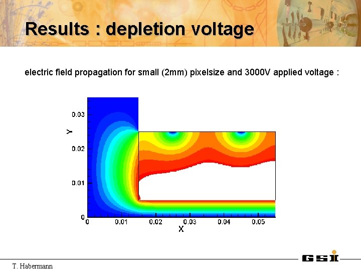
Results : depletion voltage electric field propagation for small (2 mm) pixelsize and 3000 V applied voltage : T. Habermann
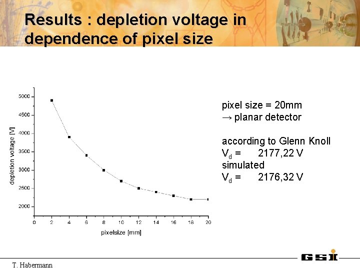
Results : depletion voltage in dependence of pixel size = 20 mm → planar detector according to Glenn Knoll Vd = 2177, 22 V simulated Vd = 2176, 32 V T. Habermann
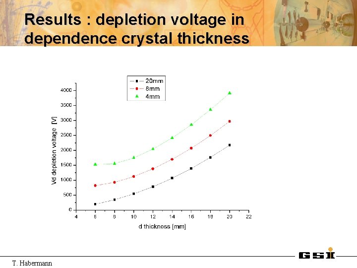
Results : depletion voltage in dependence crystal thickness T. Habermann

outlook • investigation of the electric field strength inside the germanium in dependence of pixel size, . . . • investigation of the electric field in dependence of the crystal thickness • 3 d model • another solver could be used to decrease memory usage and calculation time (essential for 3 d calculations) • . . . T. Habermann
- Slides: 22