Optical Transceivers Evaluation of Commercial Optical TRx Luis
- Slides: 19

Optical Transceivers: Evaluation of Commercial Optical TRx Luis Amaral CERN – PH/ESE/BE – Opto 10/04/2008 1

Table of Contents • • Standards; Optical Transceivers; – Form Factors; – Overview of an SFP(+) Module; – SFP+ Modules Details; • Transceiver Testing; – Transceiver Testing – SDA; • Eye Diagrams and Masks; • Characterizing Eye Diagrams; – Transceiver Testing – BERT; • BER and Rx Sensitivity; • Evaluated Transceivers; – Tx Eye Results; – TRx Numerical Results; • Single Figure of Merit; – Single FOM Results. 2

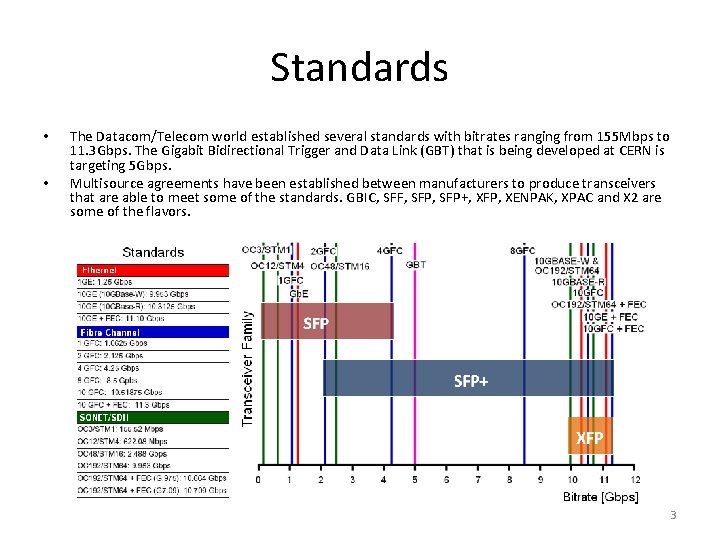
Standards • • The Datacom/Telecom world established several standards with bitrates ranging from 155 Mbps to 11. 3 Gbps. The Gigabit Bidirectional Trigger and Data Link (GBT) that is being developed at CERN is targeting 5 Gbps. Multisource agreements have been established between manufacturers to produce transceivers that are able to meet some of the standards. GBIC, SFF, SFP+, XFP, XENPAK, XPAC and X 2 are some of the flavors. 3

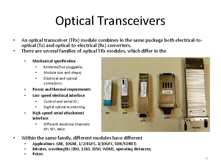
Optical Transceivers • • An optical transceiver (TRx) module combines in the same package both electrical-tooptical (Tx) and optical-to-electrical (Rx) converters. There are several families of optical TRx modules, which differ in the • Mechanical specification • Soldered/hot pluggable; • Module size and shape; • Electrical and optical connectors. • • • Power and thermal requirements Low speed electrical interface • Control and serial ID ; • Digital optical monitoring. High-speed serial attachment interface • Different electrical channels: XFI, SFI, XAUI. • Within the same family, different modules have different • • • Applications: Gb. E, 10 Gb. E, 1/2/4 GFC, 8/10 GFC, SDH/SONET; Bitrates, wavelengths (850, 1310, 1550, WDM), operating distances; Prices. 4

Form Factors • To cover the 4. 25 Gbps range there is the SFF, the GBIC and the SFP. – The SFF is a very simple TRx device that has to be soldered to the host board; – The GBIC and SFP are well established hot pluggable TRx devices; – All three devices convert one single electrical stream into one optical stream and vice-versa. • To cover the 10 Gbps range there is the 300 -pin MSA, the XENPAK (and its variants XPAK and X 2), the XFP and the SFP+. – The 300 -pin MSA module includes a Ser. Des to multiplex 16 parallel lines into one serial stream and vice-versa; – The XENPAK also avoids the 10 Gbps electrical signal problem by splitting it into 4 high-speed channels at 3. 125 Gbps with 8 b/10 b encoding; – The XFP and the SFP+ are conceptually simpler devices that do not split 10 Gbps electrical signal. • The most interesting devices are the SFP, the XFP and the SFP+. – The SFP is a small, pluggable, widespread and inexpensive(*) module but it is not specified to be used above 4. 25 Gbps; – The XFP was the first 10 Gbps version of the SFP but is bigger, expensive and power hungry. It does however include a CDR that resets the jitter and simplifies the host board design; – The SFP+ is a true SFP (same form factor) capable of covering the 10 Gbps range. This is a new device and there are three versions: Limiting, Linear and Retimed (not defined in the std). (*) especially the MM version 5

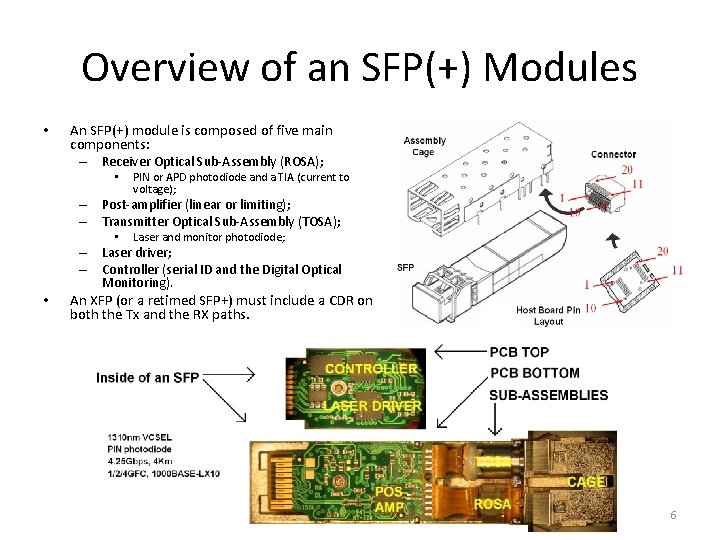
Overview of an SFP(+) Modules • An SFP(+) module is composed of five main components: – Receiver Optical Sub-Assembly (ROSA); • PIN or APD photodiode and a TIA (current to voltage); – Post-amplifier (linear or limiting); – Transmitter Optical Sub-Assembly (TOSA); • • Laser and monitor photodiode; – Laser driver; – Controller (serial ID and the Digital Optical Monitoring). An XFP (or a retimed SFP+) must include a CDR on both the Tx and the RX paths. 6

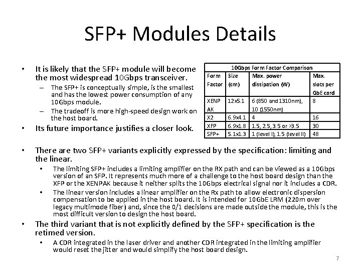
SFP+ Modules Details • It is likely that the SFP+ module will become the most widespread 10 Gbps transceiver. – The SFP+ is conceptually simple, is the smallest and has the lowest power consumption of any 10 Gbps module. – The tradeoff is more high-speed design work on the host board. 10 Gbps Form Factor Comparison Form Size Max. power Max. Factor (cm) dissipation (W) slots per Gb. E card XENP 12 x 5. 1 6 (850 and 1310 nm), 8 AK 10 (1550 nm) X 2 6. 9 x 4. 1 4 16 XFP 6. 9 x 1. 8 1. 5, 2. 5, 3. 5 or >3. 5 30 SFP+ 5. 1 x 1. 3 1 (level I), 1. 5 (level II) 48 • Its future importance justifies a closer look. • There are two SFP+ variants explicitly expressed by the specification: limiting and the linear. • • • The limiting SFP+ includes a limiting amplifier on the RX path and can be viewed as a 10 Gbps version of an SFP. It represents much more of a challenge to the host board design than the XFP or the XENPAK because it neither splits the 10 Gbps electrical signal nor it includes a CDR. The linear version includes a linear amplifier on the Rx path to allow electronic dispersion compensation to be applied in the host board. It is intended for 10 Gb. E LRM (220 m over legacy multimode fiber) and, since the 0/1 decisions are made outside the module, this is the most difficult version to design the host board. The third variant that is not explicitly defined by the SFP+ specification is the retimed version. • A CDR integrated in the laser driver and another CDR integrated in the limiting amplifier would reset the jitter and would simplify the host board design. 7

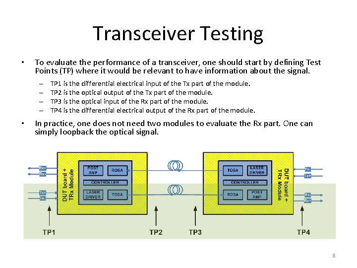
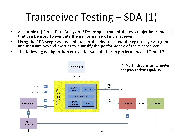
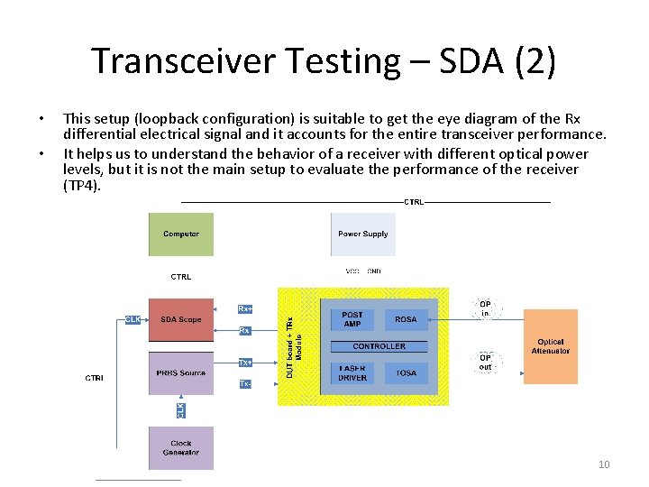
Transceiver Testing • To evaluate the performance of a transceiver, one should start by defining Test Points (TP) where it would be relevant to have information about the signal. – – • TP 1 is the differential electrical input of the Tx part of the module. TP 2 is the optical output of the Tx part of the module. TP 3 is the optical input of the Rx part of the module. TP 4 is the differential electrical output of the Rx part of the module. In practice, one does not need two modules to evaluate the Rx part. One can simply loopback the optical signal. 8

Transceiver Testing – SDA (1) • • • A suitable (*) Serial Data Analyzer (SDA) scope is one of the two major instruments that can be used to evaluate the performance of a transceiver. Using the SDA scope we are able to get the electrical and the optical eye diagrams and measure several metrics to quantify the performance of the transceiver. The following configuration is used to evaluate the Tx performance (TP 2 or TP 3). (*) Must include an optical probe and jitter analysis capability. 9

Transceiver Testing – SDA (2) • • This setup (loopback configuration) is suitable to get the eye diagram of the Rx differential electrical signal and it accounts for the entire transceiver performance. It helps us to understand the behavior of a receiver with different optical power levels, but it is not the main setup to evaluate the performance of the receiver (TP 4). 10

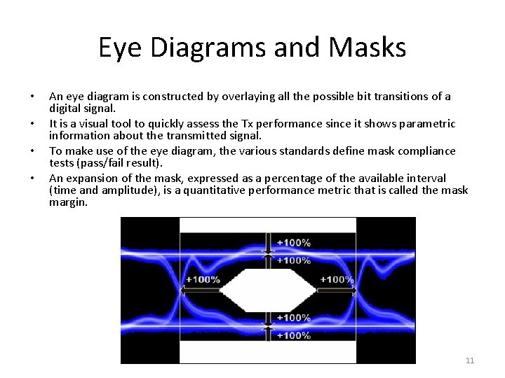
Eye Diagrams and Masks • • An eye diagram is constructed by overlaying all the possible bit transitions of a digital signal. It is a visual tool to quickly assess the Tx performance since it shows parametric information about the transmitted signal. To make use of the eye diagram, the various standards define mask compliance tests (pass/fail result). An expansion of the mask, expressed as a percentage of the available interval (time and amplitude), is a quantitative performance metric that is called the mask margin. 11

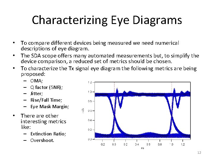
Characterizing Eye Diagrams • To compare different devices being measured we need numerical descriptions of eye diagram. • The SDA scope offers many automated measurements but, to simplify the device comparison, a reduced set of metrics should be chosen. • To characterize the Tx signal eye diagram the following metrics are being proposed: – – – OMA; Q factor (SNR); Jitter; Rise/Fall Time; Eye Mask Margin; • There are other interesting metrics like: – Extinction Ratio; – Overshoot. 12

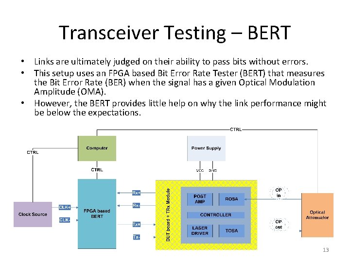
Transceiver Testing – BERT • Links are ultimately judged on their ability to pass bits without errors. • This setup uses an FPGA based Bit Error Rate Tester (BERT) that measures the Bit Error Rate (BER) when the signal has a given Optical Modulation Amplitude (OMA). • However, the BERT provides little help on why the link performance might be below the expectations. 13

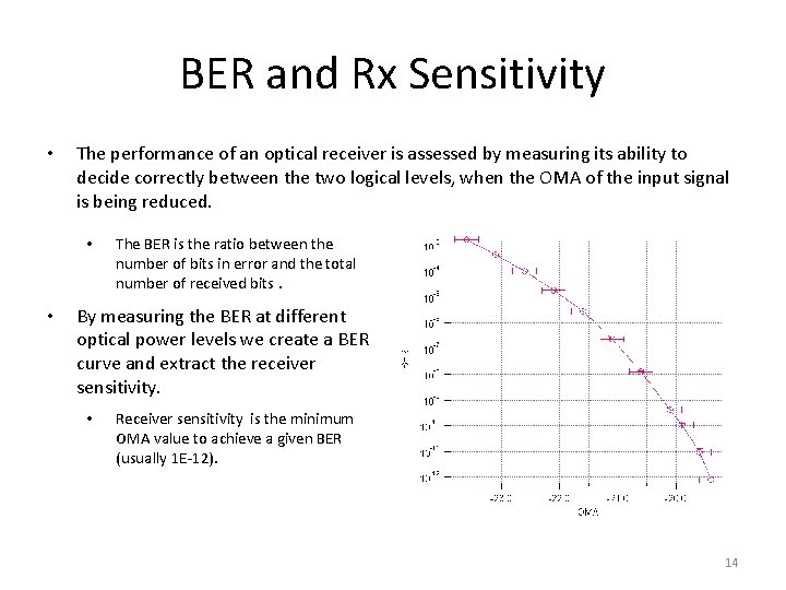
BER and Rx Sensitivity • The performance of an optical receiver is assessed by measuring its ability to decide correctly between the two logical levels, when the OMA of the input signal is being reduced. • • The BER is the ratio between the number of bits in error and the total number of received bits. By measuring the BER at different optical power levels we create a BER curve and extract the receiver sensitivity. • Receiver sensitivity is the minimum OMA value to achieve a given BER (usually 1 E-12). 14

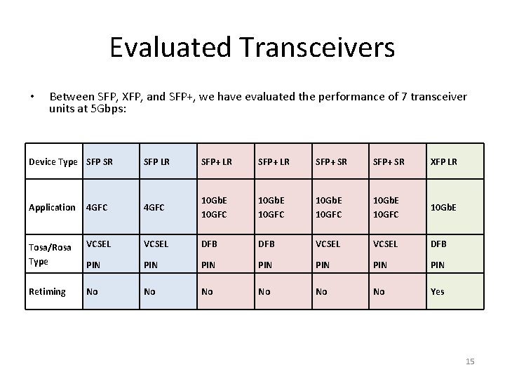
Evaluated Transceivers • Between SFP, XFP, and SFP+, we have evaluated the performance of 7 transceiver units at 5 Gbps: Device Type SFP SR SFP LR SFP+ SR XFP LR Application 4 GFC 10 Gb. E 10 GFC 10 Gb. E Tosa/Rosa Type VCSEL DFB PIN PIN Retiming No No No Yes 15

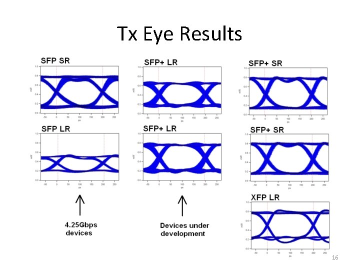
Tx Eye Results 16

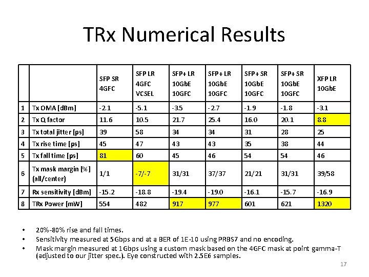
TRx Numerical Results SFP SR 4 GFC SFP LR 4 GFC VCSEL SFP+ LR 10 Gb. E 10 GFC SFP+ SR 10 Gb. E 10 GFC XFP LR 10 Gb. E 1 Tx OMA [d. Bm] -2. 1 -5. 1 -3. 5 -2. 7 -1. 9 -1. 8 -3. 1 2 Tx Q factor 11. 6 10. 5 21. 7 25. 4 16. 0 20. 1 8. 8 3 Tx total jitter [ps] 39 58 34 34 31 28 25 4 Tx rise time [ps] 45 47 43 43 35 38 44 5 Tx fall time [ps] 81 60 45 46 54 54 46 6 Tx mask margin [%] (all/center) 1/1 -7/-7 31/31 37/37 21/21 31/31 39/58 7 Rx sensitivity [d. Bm] -15. 2 -18. 8 -19. 4 -19. 0 -16. 1 -15. 7 -16. 9 8 TRx Power [m. W] 554 482 917 977 601 621 1320 • • • 20%-80% rise and fall times. Sensitivity measured at 5 Gbps and at a BER of 1 E-10 using PRBS 7 and no encoding. Mask margin measured at 1 Gbps using a custom mask based on the 4 GFC mask at point gamma-T (adjusted to our jitter spec. ). Eye constructed with 2. 5 E 6 samples. 17

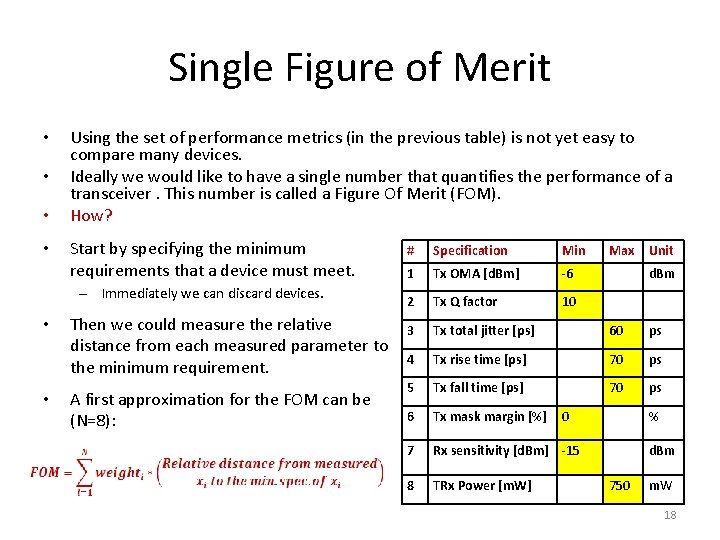
Single Figure of Merit • • Using the set of performance metrics (in the previous table) is not yet easy to compare many devices. Ideally we would like to have a single number that quantifies the performance of a transceiver. This number is called a Figure Of Merit (FOM). How? Start by specifying the minimum requirements that a device must meet. – Immediately we can discard devices. • • Then we could measure the relative distance from each measured parameter to the minimum requirement. A first approximation for the FOM can be (N=8): # Specification Min Max Unit 1 Tx OMA [d. Bm] -6 2 Tx Q factor 10 3 Tx total jitter [ps] 60 ps 4 Tx rise time [ps] 70 ps 5 Tx fall time [ps] 70 ps 6 Tx mask margin [%] 7 Rx sensitivity [d. Bm] -15 8 TRx Power [m. W] d. Bm 0 % d. Bm 750 m. W 18

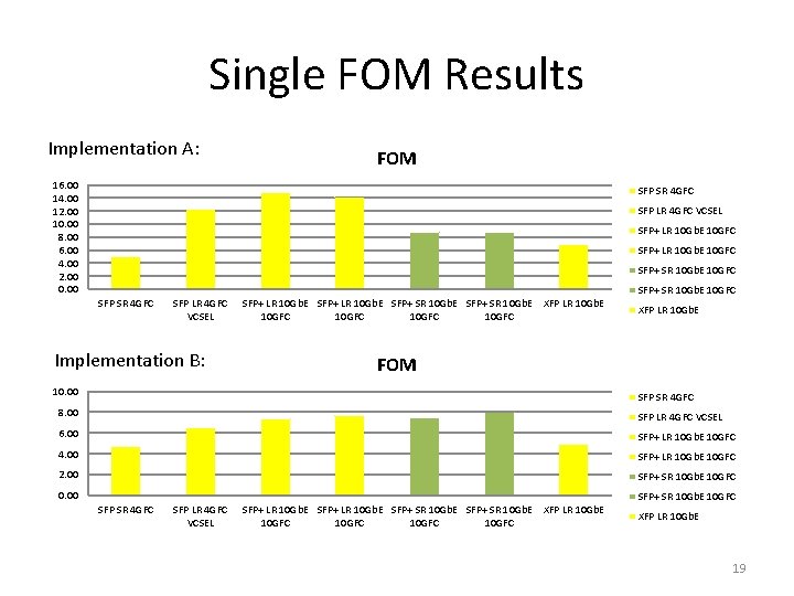
Single FOM Results Implementation A: FOM 16. 00 14. 00 12. 00 10. 00 8. 00 6. 00 4. 00 2. 00 0. 00 SFP SR 4 GFC SFP LR 4 GFC VCSEL SFP+ LR 10 Gb. E 10 GFC SFP+ SR 10 Gb. E 10 GFC SFP SR 4 GFC SFP LR 4 GFC VCSEL Implementation B: SFP+ LR 10 Gb. E SFP+ SR 10 Gb. E XFP LR 10 Gb. E 10 GFC SFP+ SR 10 Gb. E 10 GFC XFP LR 10 Gb. E FOM 10. 00 SFP SR 4 GFC 8. 00 SFP LR 4 GFC VCSEL 6. 00 SFP+ LR 10 Gb. E 10 GFC 4. 00 SFP+ LR 10 Gb. E 10 GFC 2. 00 SFP+ SR 10 Gb. E 10 GFC 0. 00 SFP SR 4 GFC SFP LR 4 GFC VCSEL SFP+ LR 10 Gb. E SFP+ SR 10 Gb. E XFP LR 10 Gb. E 10 GFC SFP+ SR 10 Gb. E 10 GFC XFP LR 10 Gb. E 19