Operational Amplifiers Op Amps a useful building block
Operational Amplifiers Op Amps – a useful building block K. El-Ayat 1
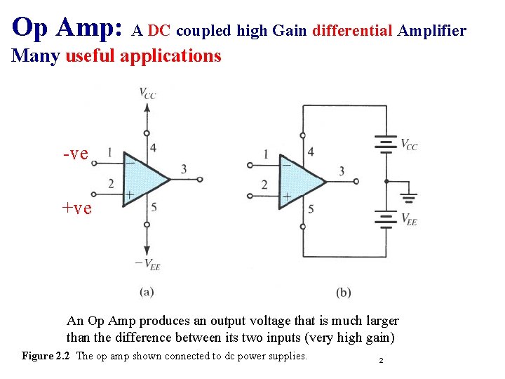
Op Amp: A DC coupled high Gain differential Amplifier Many useful applications -ve +ve An Op Amp produces an output voltage that is much larger than the difference between its two inputs (very high gain) Figure 2. 2 The op amp shown connected to dc power supplies. 2
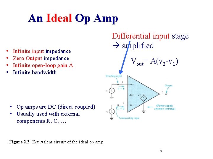
An Ideal Op Amp • • Infinite input impedance Zero Output impedance Infinite open-loop gain A Infinite bandwidth Differential input stage amplified Vout= A(v 2 -v 1) • Op amps are DC (direct coupled) • Usually used with external components R, C, … Figure 2. 3 Equivalent circuit of the ideal op amp. 3
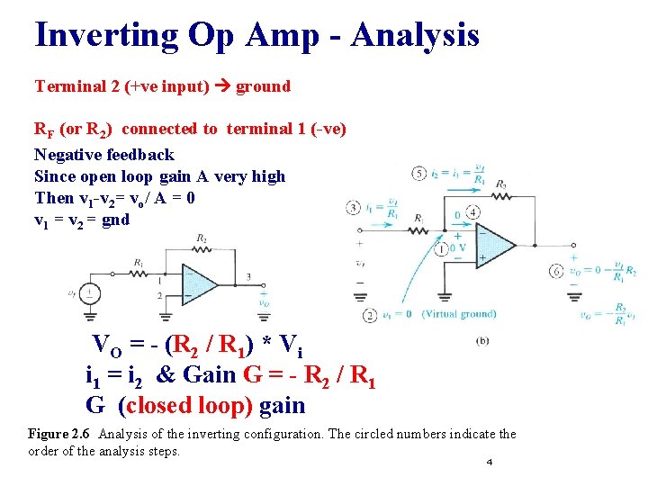
Inverting Op Amp - Analysis Terminal 2 (+ve input) ground RF (or R 2) connected to terminal 1 (-ve) Negative feedback Since open loop gain A very high Then v 1 -v 2= vo/ A = 0 v 1 = v 2 = gnd VO = - (R 2 / R 1) * Vi i 1 = i 2 & Gain G = - R 2 / R 1 G (closed loop) gain Figure 2. 6 Analysis of the inverting configuration. The circled numbers indicate the order of the analysis steps. 4
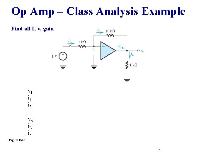
Op Amp – Class Analysis Example Find all I, v, gain v 1 = i 2 = vo = i. L = io = Figure E 2. 6 5
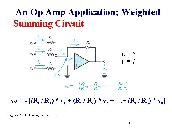
An Op Amp Application; Weighted Summing Circuit in = ? i =? vo = - [(Rf / R 1) * v 1 + (Rf / R 2) * v 2 +…. + (Rf / Rn) * vn] Figure 2. 10 A weighted summer. 6
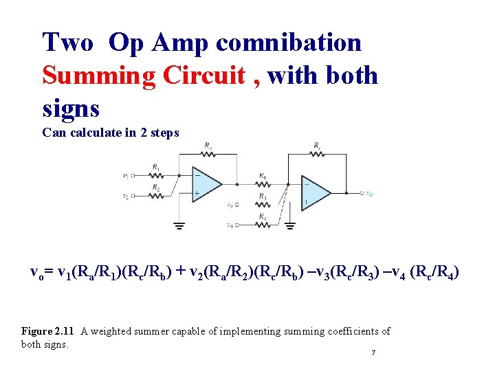
Two Op Amp comnibation Summing Circuit , with both signs Can calculate in 2 steps vo= v 1(Ra/R 1)(Rc/Rb) + v 2(Ra/R 2)(Rc/Rb) –v 3(Rc/R 3) –v 4 (Rc/R 4) Figure 2. 11 A weighted summer capable of implementing summing coefficients of both signs. 7
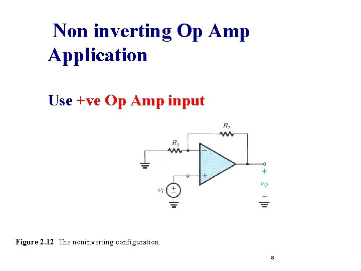
Non inverting Op Amp Application Use +ve Op Amp input Figure 2. 12 The noninverting configuration. 8
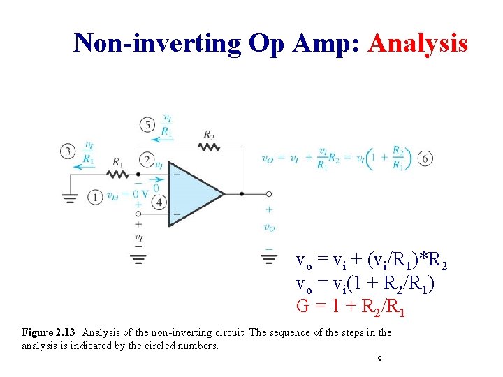
Non-inverting Op Amp: Analysis vo = vi + (vi/R 1)*R 2 vo = vi(1 + R 2/R 1) G = 1 + R 2/R 1 Figure 2. 13 Analysis of the non-inverting circuit. The sequence of the steps in the analysis is indicated by the circled numbers. 9
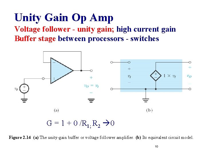
Unity Gain Op Amp Voltage follower - unity gain; high current gain Buffer stage between processors - switches G = 1 + 0 /R 1; R 2 0 Figure 2. 14 (a) The unity-gain buffer or voltage follower amplifier. (b) Its equivalent circuit model. 10
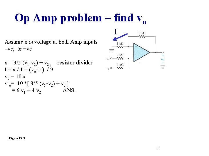
Op Amp problem – find vo I Assume x is voltage at both Amp inputs –ve, & +ve x = 3/5 (v 1 -v 2) + v 2 ; resistor divider I = x / 1 = (vo- x) / 9 vo = 10 x v o= 10 *[ 3/5 (v 1 -v 2) + v 2 ] = 6 v 1 + 4 v 2 ANS. Figure E 2. 9 11
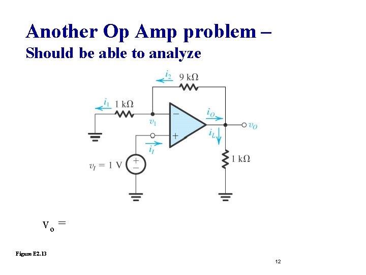
Another Op Amp problem – Should be able to analyze vo = Figure E 2. 13 12
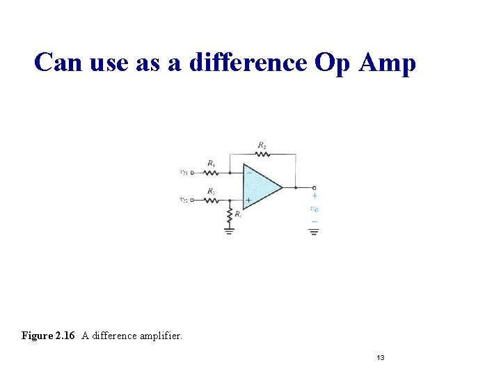
Can use as a difference Op Amp Figure 2. 16 A difference amplifier. 13
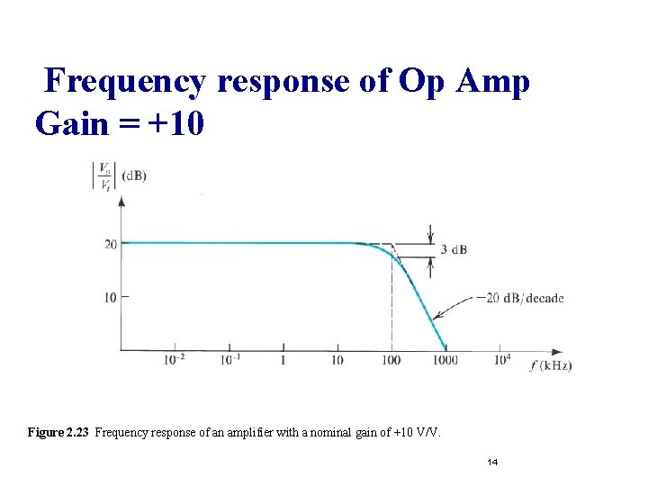
Frequency response of Op Amp Gain = +10 Figure 2. 23 Frequency response of an amplifier with a nominal gain of +10 V/V. 14
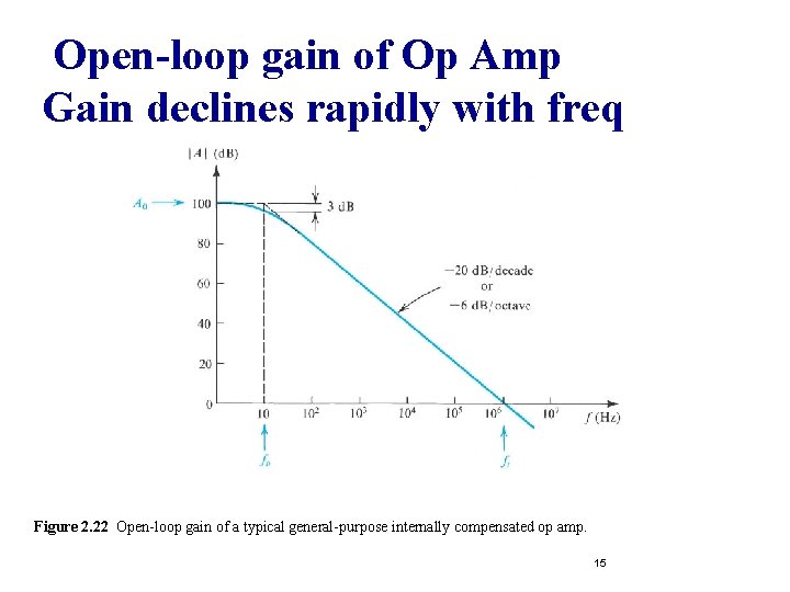
Open-loop gain of Op Amp Gain declines rapidly with freq Figure 2. 22 Open-loop gain of a typical general-purpose internally compensated op amp. 15
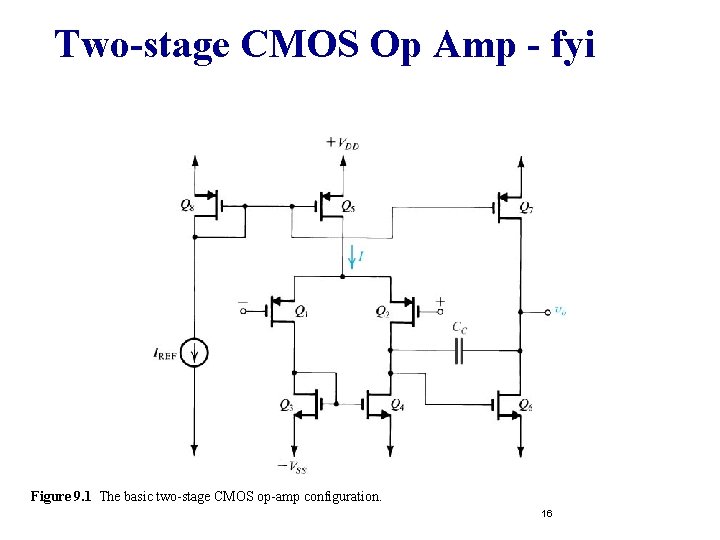
Two-stage CMOS Op Amp - fyi Figure 9. 1 The basic two-stage CMOS op-amp configuration. 16
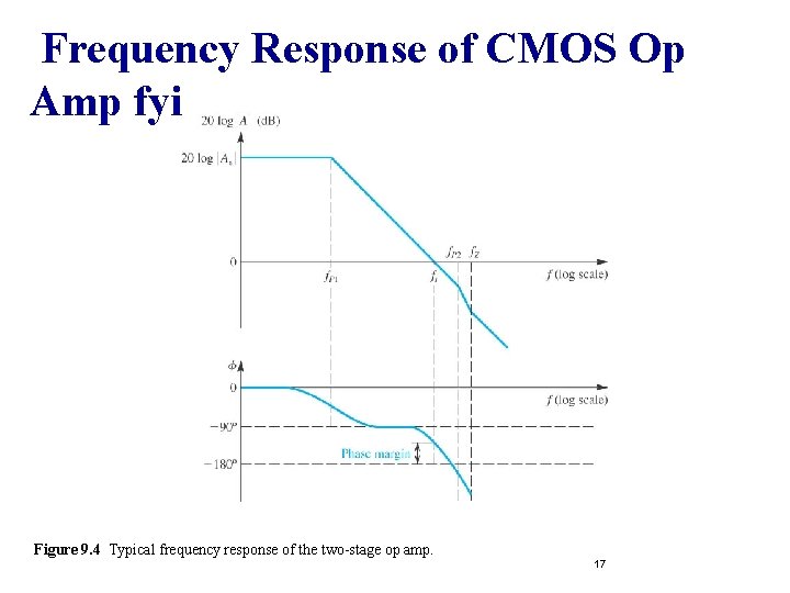
Frequency Response of CMOS Op Amp fyi Figure 9. 4 Typical frequency response of the two-stage op amp. 17
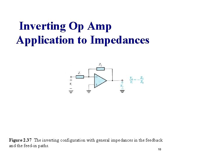
Inverting Op Amp Application to Impedances Figure 2. 37 The inverting configuration with general impedances in the feedback and the feed-in paths. 18
- Slides: 18