
Open NVM An OpenSourced FPGAbased NVM Controller for
Open. NVM: An Open-Sourced FPGA-based NVM Controller for Low Level Memory Characterization Jie Zhang 1, Gieseo Park 2, Mustafa M Shihab 2, David Donofrio 3, John Shalf 3, and Myoungsoo Jung 1 1 School of Integrated Technology, Yonsei University 2 Department of EE, The University of Texas at Dallas 3 Computer Architecture Laboratory, Lawrence Berkeley National Laboratory 33 rd IEEE International Conference on Computer Design ICCD 2015
Executive Summary Motivation Emerging NVMs have demonstrated immense potential for addressing the challenges faced by existing memory technologies, in terms of – density, latency, and power/energy consumption Challenge Existing NVM research is mainly confined to theoretical models and simulation data that can fluctuate from real products. There is a growing need for publicly available IPs(intellectual property) for evaluating new NVMs Proposal Open. NVM: An open-sourced platform for evaluating NVM devices ü Empirically evaluates real NVM products ü Supports different NVMs using the same hardware platform ü Freely available to the research community Evaluation Results q TLC NAND: Latency, Power, and Error analysis q MRAM: Validation, Current and Power/Energy consumption 33 rd IEEE International Conference on Computer Design ICCD 2015

NVMs are shaping the future Wide range of NVMs have been successfully developed in recent years: q Flash-based NVMs: NOR flash, NAND flash (SLC/MLC/TLC) q Memristor-based NVMs: MRAM, PCM, RRAM, etc. These NVMs show great potential for: üDelivering better density, latency, and power/energy consumption üProviding a smooth technological transition by fitting into the different layers of the existing memory hierarchy…. Cache, Main Memory, Secondary Storage, and overlapping applications such as Storage Class Memory 33 rd IEEE International Conference on Computer Design ICCD 2015
Open. NVM q. NVMs are being researched extensively, but predominantly based on analytic models and simulation data …. Which can critically vary from real products q. The main bottleneck is the absence of publicly available IPs for NVM controllers q. The next leap for NVM research requires üDevising an open platform for collecting NVM data from real products üMaking that platform flexible - to allow evaluation of different NVMs with minimal cost (hardware and software) for switching between technologies We present Open. NVM! q. FPGA-based platform for: üAccurate empirical characterization of real NVM products under practical working condition üSupports a wide range of NVM technology q. Open-sourced technology: Developed to be a research vehicle for the non-commercial NVM research community 33 rd IEEE International Conference on Computer Design ICCD 2015

Architecture q q Host: Conventional personal computer FPGA: Diligent Nexys 3 (based on Xilinx Spartan 6) Daughterboard: connects NVM pins to FPGA pins Power Board: measures average current 33 rd IEEE International Conference on Computer Design ICCD 2015
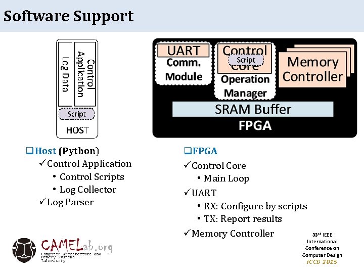
Software Support q. Host (Python) üControl Application • Control Scripts • Log Collector üLog Parser q. FPGA üControl Core • Main Loop üUART • RX: Configure by scripts • TX: Report results üMemory Controller 33 rd IEEE International Conference on Computer Design ICCD 2015
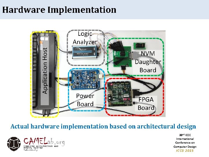
Hardware Implementation Actual hardware implementation based on architectural design 33 rd IEEE International Conference on Computer Design ICCD 2015
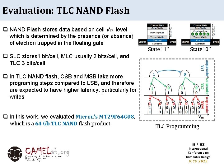
Evaluation: TLC NAND Flash q NAND Flash stores data based on cell VT h level which is determined by the presence (or absence) of electron trapped in the floating gate State “ 1” State “ 0” q SLC stores 1 bit/cell, MLC usually 2 bits/cell, and TLC 3 bits/cell q In TLC NAND flash, CSB and MSB take more programing steps compared to LSB, and therefore are expected to have higher latency, particularly for writes q In this work, we evaluated Micron’s MT 29 F 64 G 08, which is a 64 Gb TLC NAND flash product TLC Programming 33 rd IEEE International Conference on Computer Design ICCD 2015
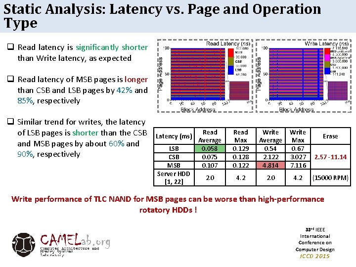
Static Analysis: Latency vs. Page and Operation Type q Read latency is significantly shorter than Write latency, as expected q Read latency of MSB pages is longer than CSB and LSB pages by 42% and 85%, respectively q Similar trend for writes, the latency of LSB pages is shorter than the CSB and MSB pages by about 60% and 90%, respectively Latency (ms) LSB CSB MSB Server HDD [1, 22] Read Average 0. 058 0. 075 0. 107 Read Max 0. 129 0. 128 0. 122 Write Average 0. 54 2. 122 4. 814 Write Max 0. 67 3. 027 7. 116 2. 0 4. 2 Erase 2. 57 -11. 14 (15000 RPM) Write performance of TLC NAND for MSB pages can be worse than high-performance rotatory HDDs ! 33 rd IEEE International Conference on Computer Design ICCD 2015
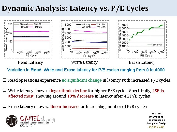
Dynamic Analysis: Latency vs. P/E Cycles Read Latency Write Latency Erase Latency Variation in Read, Write and Erase latency for P/E cycles ranging from 0 to 4000 q Read operations experience no significant change in latency with increased P/E cycles q Write latency shows a logarithmic decline for higher P/E cycles. Specifically, LSB is affected most, showing around 18% decrease in latency after 4 K P/E cycles q Erase latency shows a linear increase for increasing number of P/E cycles 33 rd IEEE International Conference on Computer Design ICCD 2015
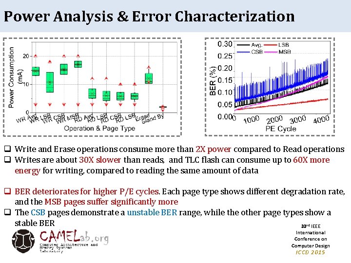
Power Analysis & Error Characterization q Write and Erase operations consume more than 2 X power compared to Read operations q Writes are about 30 X slower than reads, and TLC flash can consume up to 60 X more energy for writing, compared to reading the same amount of data q BER deteriorates for higher P/E cycles. Each page type shows different degradation rate, and the MSB pages suffer significantly more q The CSB pages demonstrate a unstable BER range, while the other page types show a stable BER 33 IEEE rd International Conference on Computer Design ICCD 2015
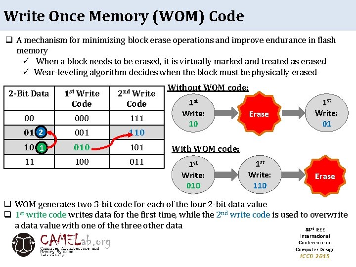
Write Once Memory (WOM) Code q A mechanism for minimizing block erase operations and improve endurance in flash memory ü When a block needs to be erased, it is virtually marked and treated as erased ü Wear-leveling algorithm decides when the block must be physically erased 2 -Bit Data 1 st Write Code 2 nd Write Code 00 000 111 01 2 001 110 10 1 010 101 11 100 011 Without WOM code: 1 st Write: 10 Erase 1 st Write: 01 1 st Write: 110 Erase With WOM code: 1 st Write: 010 q WOM generates two 3 -bit code for each of the four 2 -bit data value q 1 st write code writes data for the first time, while the 2 nd write code is used to overwrite a data value with one of the three other data 33 IEEE rd International Conference on Computer Design ICCD 2015
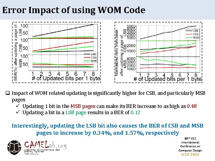
Error Impact of using WOM Code q Impact of WOM related updating is significantly higher for CSB, and particularly MSB pages ü Updating 1 bit in the MSB pages can make its BER increase to as high as 0. 48 ü Updating a bit in a LSB page results in a BER of 0. 12 Interestingly, updating the LSB bit also causes the BER of CSB and MSB pages to increase by 0. 34%, and 1. 57%, respectively 33 rd IEEE International Conference on Computer Design ICCD 2015
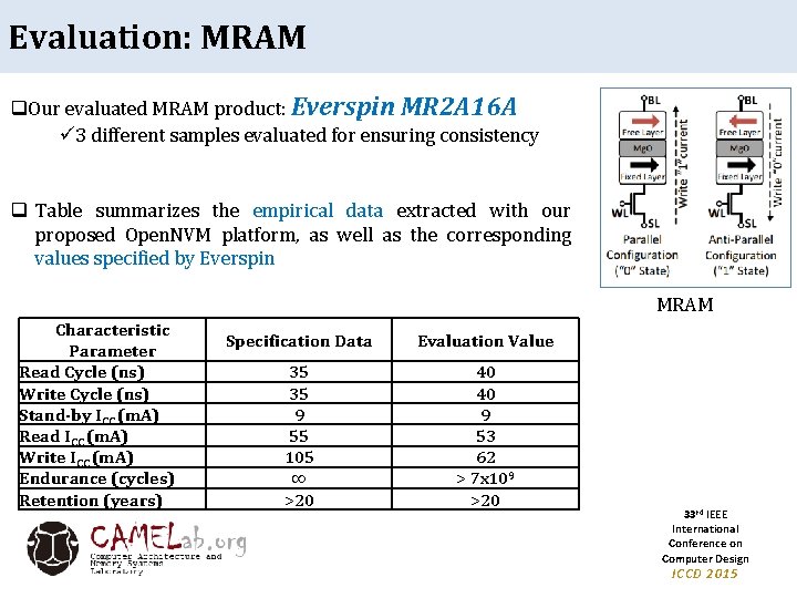
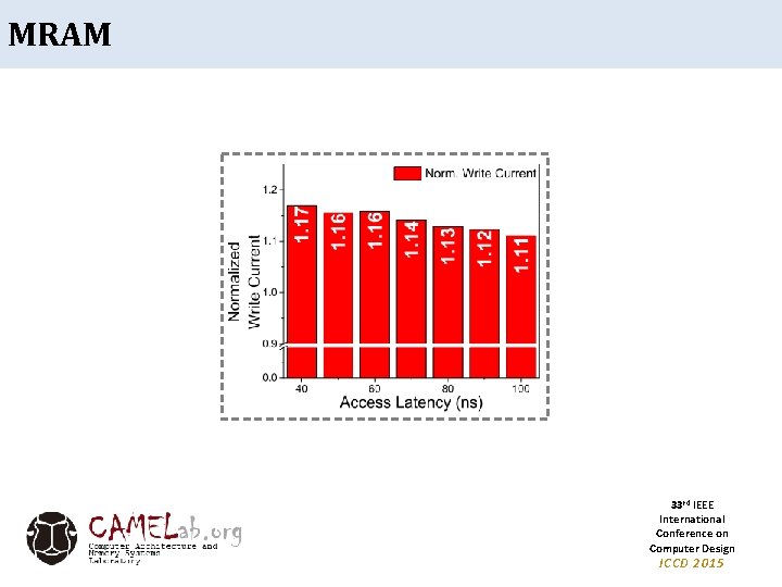
Evaluation: MRAM q. Our evaluated MRAM product: Everspin MR 2 A 16 A ü 3 different samples evaluated for ensuring consistency q Table summarizes the empirical data extracted with our proposed Open. NVM platform, as well as the corresponding values specified by Everspin MRAM Characteristic Parameter Read Cycle (ns) Write Cycle (ns) Stand-by ICC (m. A) Read ICC (m. A) Write ICC (m. A) Endurance (cycles) Retention (years) Specification Data Evaluation Value 35 35 9 55 105 ∞ >20 40 40 9 53 62 > 7 x 10⁹ >20 33 rd IEEE International Conference on Computer Design ICCD 2015
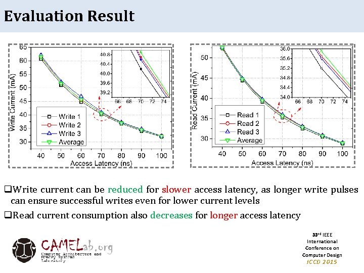
Evaluation Result q. Write current can be reduced for slower access latency, as longer write pulses can ensure successful writes even for lower current levels q. Read current consumption also decreases for longer access latency 33 rd IEEE International Conference on Computer Design ICCD 2015
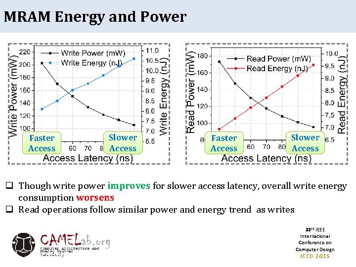
MRAM Energy and Power Faster Access Slower Access q Though write power improves for slower access latency, overall write energy consumption worsens q Read operations follow similar power and energy trend as writes 33 rd IEEE International Conference on Computer Design ICCD 2015
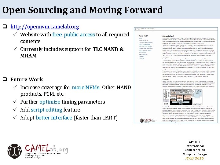
Open Sourcing and Moving Forward q http: //opennvm. camelab. org ü Website with free, public access to all required contents ü Currently includes support for TLC NAND & MRAM q Future Work ü Increase coverage for more NVMs: Other NAND products, PCM, etc. ü Further optimize timing parameters ü Add script editing feature ü Adopt better interface (faster than UART) 33 rd IEEE International Conference on Computer Design ICCD 2015
References and Related Work “MR 2 A 16 A, ” http: //goo. gl/Sdvjy. V, Everspin Technologies “MT 29 F 64 G 08, ” http: //goo. gl/GXV 5 Qq, Micron “Nexys 3 - Reference Manual, ” https: //goo. gl/Ok 08 j. V, Digilent Inc R. Gabrys et al. , “Non-binary wom-codes for multilevel flash memories, ” in ITW, 2011 § Smullen, C. W. ; Mohan, V. ; Nigam, A. ; Gurumurthi, S. and Stan, M. R. , “Relaxing non-volatility for fast and energy-efficient STT-RAM caches”, HPCA 2011 § Qureshi, M. K. ; Srinivasan, V. and Rivers, J. A. , “Scalable high performance main memory system using phase-change memory technology”, SIGARCH 2009 § Mangalagiri, P. ; Sarpatwari, K. ; Yanamandra, A. ; Narayanan, V. ; Xie, Y. ; Irwin, M. J. and Karim, O. A. , “A low-power phase change memory based hybrid cache architecture”, GLSVLSI 2008 § § 33 rd IEEE International Conference on Computer Design ICCD 2015

Thank You 33 rd IEEE International Conference on Computer Design ICCD 2015
Back Up Slides 33 rd IEEE International Conference on Computer Design ICCD 2015
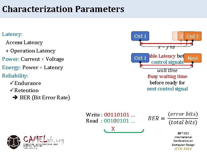
Characterization Parameters Latency: Access Latency + Operation Latency Power: Current × Voltage Energy: Power × Latency Reliability: üEndurance üRetention BER (Bit Error Rate) Ctrl 2 Ctrl 1 x ~ y ns Variable Latency between Ctrl 1 Next control signals wait time Busy waiting time before ready for next control signal Write : 00110101 … Read : 00100101 … X 33 rd IEEE International Conference on Computer Design ICCD 2015
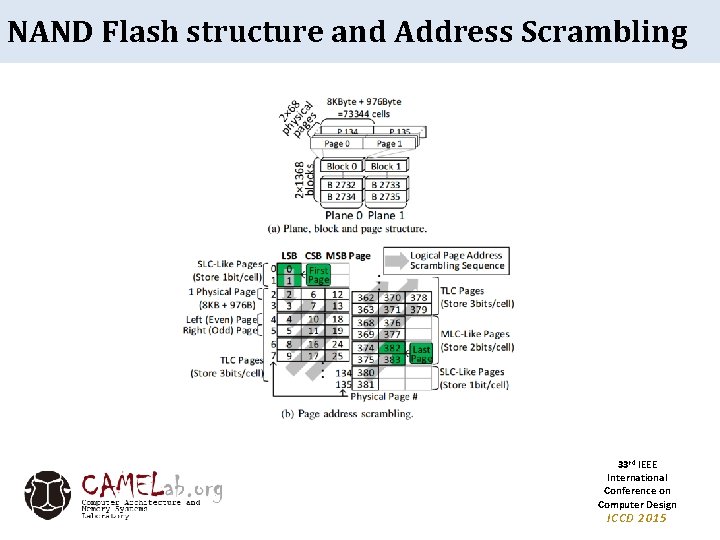
NAND Flash structure and Address Scrambling 33 rd IEEE International Conference on Computer Design ICCD 2015
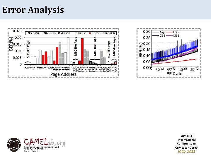
Error Analysis 33 rd IEEE International Conference on Computer Design ICCD 2015
MRAM 33 rd IEEE International Conference on Computer Design ICCD 2015
- Slides: 24