
Open Coherent Accelerator Processor Interface TM Open CAPI




- Slides: 17
Open Coherent Accelerator Processor Interface TM Open. CAPI - A New Standard for High Performance Memory, Acceleration and Networks Jeff Stuecheli April 10, 2017
What is Open CAPI • Device attach • • • Memory Accelerators Network Storage Etc. • Latency: 10 s of ns interface overhead • Bandwidth: 25 G+ differential signaling • Flexibility: One interface scaling from low latency memory to sophisticated accelerators
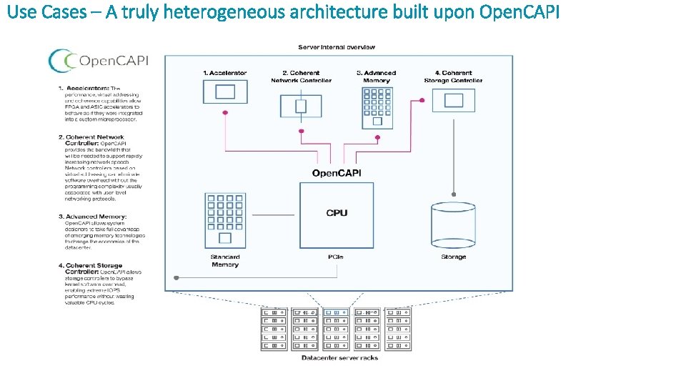
Use Cases – A truly heterogeneous architecture built upon Open. CAPI
Asymmetric Design Philosophy • Motivation • Simplify accelerator to enable 1. 2. 3. 4. Host ISA agnostic Contain coherence complexity to host silicon Higher performance as logic in host silicon higher perf than accelerator Contain accelerator in sandbox to enable fault tolerance and security
Importance of Latency • Server memory latency is critical TOC factor • Differential solution must provide ~equivalent effective latency of DDR standards • POWER 8 DMI round trip latency 10 ns • Typical PCIe round trip latency ~100 s ns • Why is DMI so low? • DMI designed from ground up for minimum latency due to ld/str requirements • Open CAPI key concept • Provide DMI like latency, but with enhanced command set of CAPI
Comparison of Acceleration Paradigms Memory Transform DLx/TLx Egress Transform Acc Processor Chip Example: Basic offload Data Processor Chip Examples: Machine Learning, Deep Learning potentially using Open. CAPI attached memory DLx/TLx Data Examples: Encryption, Compression, Erasure prior to network or storage Ingress Transform Acc Processor Chip DLx/TLx Data Examples: Video Analytics, HFT, VPN/IPsec/SSL, Deep Packet Inspection (DPI), Data Plane Accelerator (DPA), Video Encoding (H. 265) etc Bi-Directional Transform Acc Needle-In-A-Haystack. Engine Needle-in-a-haystack Processor Chip DLx/TLx Needles Examples: Database searches, joins, intersections, merges Acc Haystack Data Processor Chip TLx/DLx Data Acc Examples: No. SQL such as Neo 4 J with Graph Node Traversals etc 6
Comparison of Memory Paradigms Main Memory DLx/TLx Data DDR 4/5 Processor Chip Example: Basic DDR attach Emerging Memory SCM Processor Chip Tiered Memory Needle-in-a-haystack Engine DLx/TLx Data SCM DLx/TLx DDR 4/5 Processor Chip 7
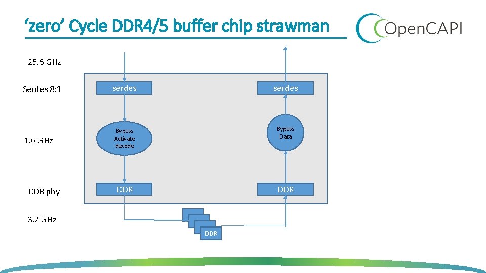
‘zero’ Cycle DDR 4/5 buffer chip strawman 25. 6 GHz Serdes 8: 1 1. 6 GHz DDR phy serdes Bypass Activate decode Bypass Data DDR 3. 2 GHz DDR
Simplified High Performance Accelerator • Explicit command templates enable extremely simple command decode • For best latency CRC bypass • Virtual address based cache enables simplified parallel accelerator caching structures based around data structure semantics (rather than typical Von Neumann bottleneck)
Host scalability • Asymmetric design isolated host coherence throughput from accelerator (avoid scenario of plugging a card or flashing an FPGA image slowing entire system). • Ground up high throughput design with explicit memory barriers enables efficient host implementation (rather than overly strict PCIe). • Open CAPI optimized serdes significant power+area advantage over PCIe enables higher IO bw
Virtual Addressing Ø An Open. CAPI device operates in the virtual address spaces of the applications that it supports Ø Eliminates kernel and device driver software overhead Ø Improves accelerator performance Ø Allows device to operate directly on application memory without kernel-level data copies or pinned pages Ø Simplifies programming effort to integrate accelerators into applications Ø The Virtual-to-Physical Address Translation occurs in the host CPU Ø Reduces design complexity of Open. CAPI-attached devices Ø Makes it easier to ensure interoperability between an Open. CAPI device and multiple CPU architectures Ø Since the Open. CAPI device never has access to a physical address, this eliminates the possibility of a defective or malicious device accessing memory locations belonging to the kernel or other applications that it is not authorized to access
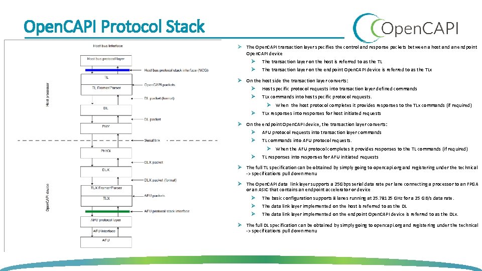
Open. CAPI Protocol Stack Ø The Open. CAPI transaction layer specifies the control and response packets between a host and an endpoint Open. CAPI device Ø Ø The transaction layer on the host is referred to as the TL The transaction layer on the endpoint Open. CAPI device is referred to as the TLx Ø On the host side the transaction layer converts: Ø Host specific protocol requests into transaction layer defined commands Ø TLx commands into host specific protocol requests. Ø When the host protocol completes it provides responses to the TLx commands (if required) Ø TLx responses into responses for host initiated requests Ø On the endpoint Open. CAPI device, the transaction layer converts: Ø AFU protocol requests into transaction layer commands Ø TL commands into AFU protocol requests. Ø When the AFU protocol completes it provides responses to the TL commands (if required) Ø TL responses into responses for AFU initiated requests Ø The full TL specification can be obtained by simply going to opencapi. org and registering under the technical -> specifications pull down menu Ø The Open. CAPI data link layer supports a 25 Gbps serial data rate per lane connecting a processor to an FPGA or an ASIC that contains an endpoint accelerator or device Ø The basic configuration supports 8 lanes running at 25. 78125 GHz for a 25 GB/s data rate. Ø The data link layer implemented on the host is referred to as the DL Ø The data link layer implemented on the endpoint Open. CAPI device is referred to as the DLx. Ø The full DL specification can be obtained by simply going to opencapi. org and registering under the technical -> specifications pull down menu
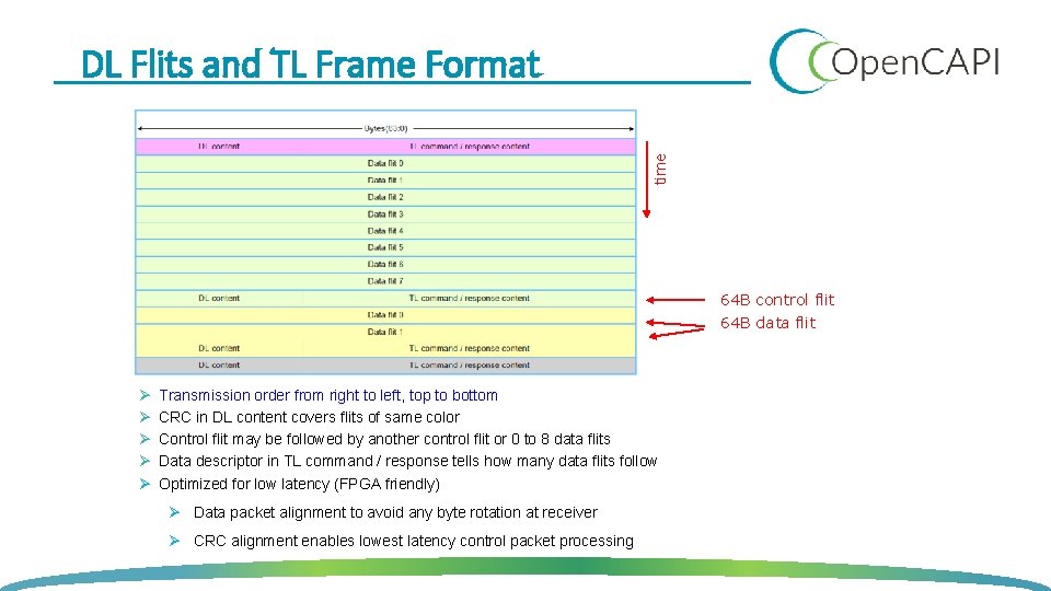
September IBM + Google Technical Meeting time DL Flits and TL Frame Format 64 B control flit 64 B data flit Ø Ø Ø Transmission order from right to left, top to bottom CRC in DL content covers flits of same color Control flit may be followed by another control flit or 0 to 8 data flits Data descriptor in TL command / response tells how many data flits follow Optimized for low latency (FPGA friendly) Ø Data packet alignment to avoid any byte rotation at receiver Ø CRC alignment enables lowest latency control packet processing
25 Gbit PHY Ø Open CAPI is agnostic to processor architecture and as such the electrical interface is not being defined by the Open. CAPI consortium or any of its workgroups Ø However if a partner wishes to connect with IBM’s Power 9 microprocessor the electrical interface is defined as follows Ø Definition is being driven by the 25 G workgroup within the Open. Power Foundation Ø Based on the OIF CEI 28 G SR specification Ø 25 Gbit/sec signaling and protocol built to enable very low latency interface on CPU and attached device Ø Allows for future looking media improvements such as 32 Gb/s and 56 Gb/s signaling
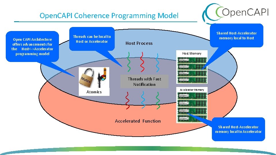
Open. CAPI Coherence Programming Model Open CAPI Architecture offers advancements for the Host<->Accelerator programming model Threads can be local to Host or Accelerator Shared Host-Accelerator memory local to Host Process Host Memory Threads with Fast Notification Accelerator Memory Atomics Accelerated Function Shared Host-Accelerator memory local to Accelerator
FPGA versus ASIC/Structured Array Ø The Open. CAPI architecture is truly agnostic to a specific vendor technology Ø The TLx and DLx reference RTL is written for the Xilinx FPGA Vivado toolchain and statistics are provided using that flow in this deck Ø BRAM(s), Distributed RAM(s) are specific Xilinx constructs Ø To convert to an ASIC vendor or a structured array technology would be a very minimal exercise to port Ø Discussions have been held to take our reference RTL and harden it into a structured array technology Ø Master Definition is underway between IBM and Toshiba Ø Economy of scale and NRE are considerations that partners need to make in deciding whether to go the FPGA, ASIC, or structured array route to market
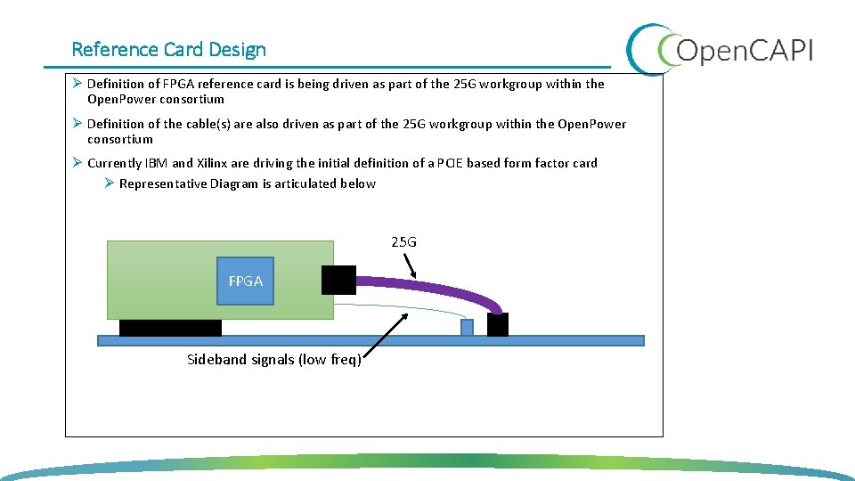
Reference Card Design Ø Definition of FPGA reference card is being driven as part of the 25 G workgroup within the Open. Power consortium Ø Definition of the cable(s) are also driven as part of the 25 G workgroup within the Open. Power consortium Ø Currently IBM and Xilinx are driving the initial definition of a PCIE based form factor card Ø Representative Diagram is articulated below 25 G FPGA Sideband signals (low freq) 17