OPA 2227 All NPN Output Stage Analysis Precision


- Slides: 21

OPA 2227 All NPN Output Stage Analysis Precision Linear Analog Applications April 19 th, 2018 – Tim Green, Thomas Kuehl 1

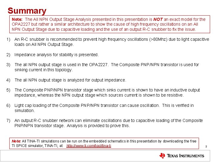
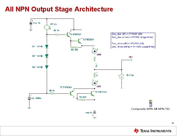
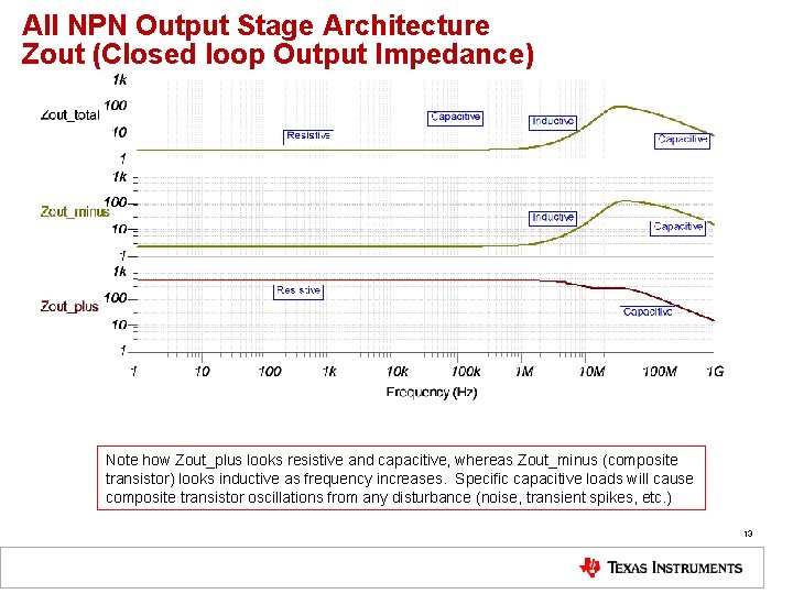
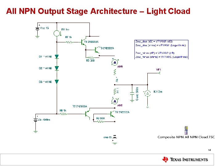
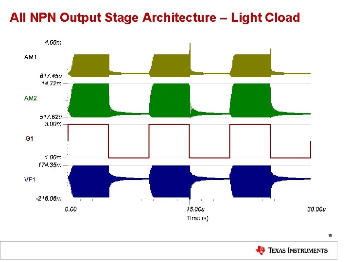
Summary Note: The All NPN Output Stage Analysis presented in this presentation is NOT an exact model for the OPA 2227 but rather a similar architecture to show the cause of high frequency oscillations on an All NPN Output Stage due to capacitive loading and the use of an output R-C snubber to fix the issue. 1) An R-C snubber is recommended to prevent high frequency oscillations (>80 Mhz) due to light capacitive loads on All NPN Output Stage. 2) Impedance analysis for stability is presented. 3) The all NPN output stage is used in the OPA 2227. The Composite PNP/NPN transistor is used for sinking current in this topology. 4) The all NPN output stage is analyzed for output impedance. 5) The Composite PNP/NPN transistor stage which sinks current is shown to have an inductive output impedance, whereas the NPN output stage which sources current is shown to be resistive. 6) Light cap loading of the Composite PNP/NPN transistor can cause oscillation. This is verified in simulation. 7) An output R-C snubber network can eliminate oscillations due to capacitive loading of the Composite PNP/NPN transistor stage. Analysis is provided to prove this. Note: All TINA-TI simulations can be run on the embedded schematics in this presentation by downloading the free TI SPICE simulator, TINA-TI, at: http: //www. ti. com/tool/tina-ti 2

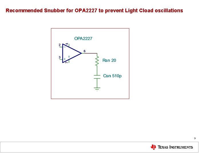
Recommended Snubber for OPA 2227 to prevent Light Cload oscillations 3

Impedance Analysis for Stability 4

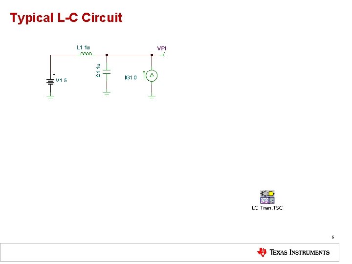
Typical L-C Circuit 5

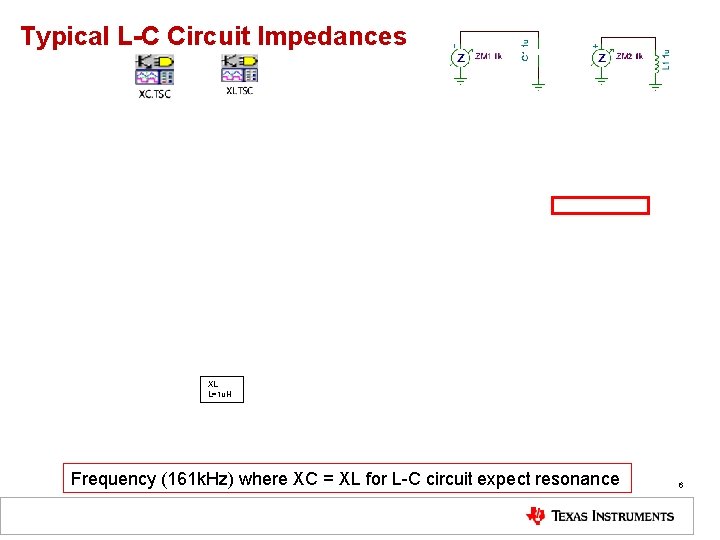
Typical L-C Circuit Impedances XL L=1 u. H Frequency (161 k. Hz) where XC = XL for L-C circuit expect resonance 6

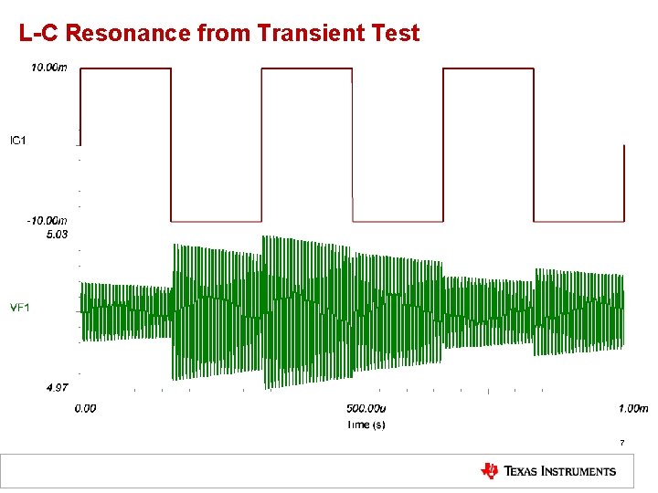
L-C Resonance from Transient Test 7

L-C Resonance from Transient Test Transient Resonance at Frequency (161 k. Hz) where XC = XL predicted L-C circuit resonance 8

Technical Reference: Closed Loop Impedance Stability Analysis (embedded pdf document) 9

OPA 2227 All NPN Output Stage Analysis 10

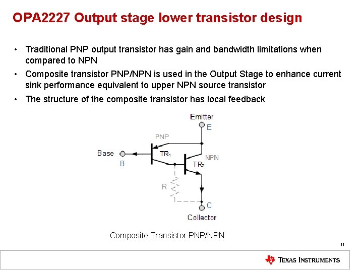
OPA 2227 Output stage lower transistor design • Traditional PNP output transistor has gain and bandwidth limitations when compared to NPN • Composite transistor PNP/NPN is used in the Output Stage to enhance current sink performance equivalent to upper NPN source transistor • The structure of the composite transistor has local feedback Composite Transistor PNP/NPN 11

All NPN Output Stage Architecture 12

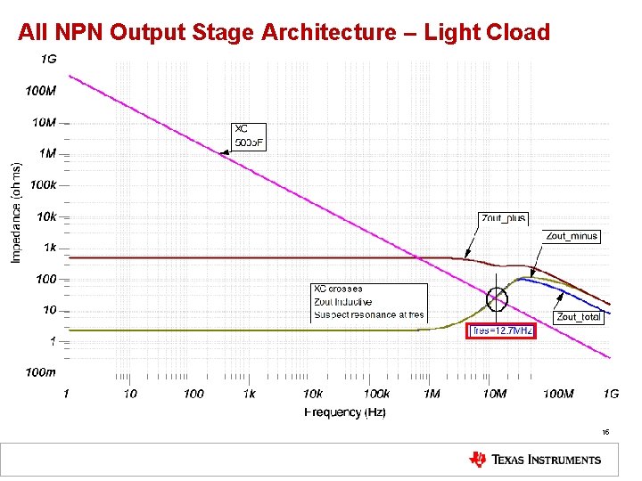
All NPN Output Stage Architecture Zout (Closed loop Output Impedance) Note how Zout_plus looks resistive and capacitive, whereas Zout_minus (composite transistor) looks inductive as frequency increases. Specific capacitive loads will cause composite transistor oscillations from any disturbance (noise, transient spikes, etc. ) 13

All NPN Output Stage Architecture – Light Cload 14

All NPN Output Stage Architecture – Light Cload 15

All NPN Output Stage Architecture – Light Cload 16

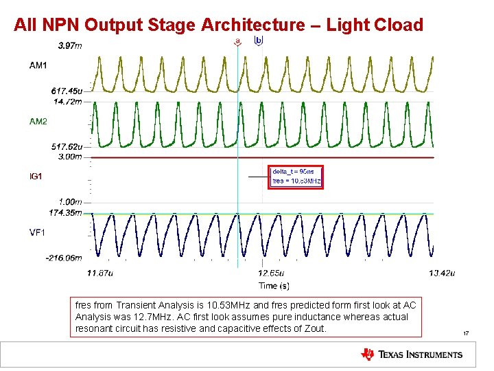
All NPN Output Stage Architecture – Light Cload fres from Transient Analysis is 10. 53 MHz and fres predicted form first look at AC Analysis was 12. 7 MHz. AC first look assumes pure inductance whereas actual resonant circuit has resistive and capacitive effects of Zout. 17

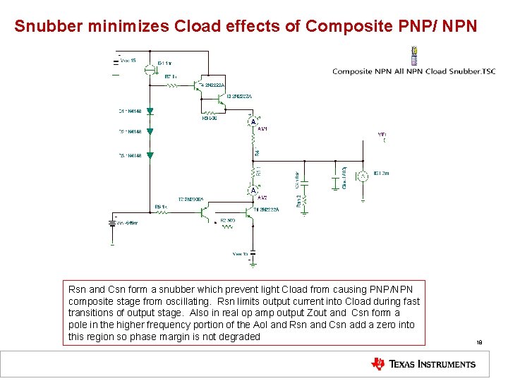
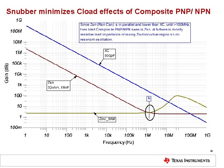
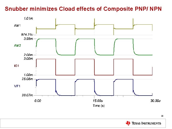
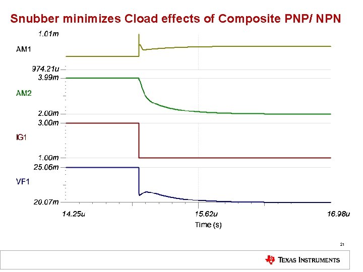
Snubber minimizes Cload effects of Composite PNP/ NPN Rsn and Csn form a snubber which prevent light Cload from causing PNP/NPN composite stage from oscillating. Rsn limits output current into Cload during fast transitions of output stage. Also in real op amp output Zout and Csn form a pole in the higher frequency portion of the Aol and Rsn and Csn add a zero into this region so phase margin is not degraded 18

Snubber minimizes Cload effects of Composite PNP/ NPN 19

Snubber minimizes Cload effects of Composite PNP/ NPN 20

Snubber minimizes Cload effects of Composite PNP/ NPN 21