Op Amp Specifications What do they mean How
- Slides: 40

Op Amp Specifications What do they mean? How do we test them? Keith Kendall & Bruce Trump Including Portions from the Bruce Trump & Gina Hann 2 -Op Amp Loop Presentation 1

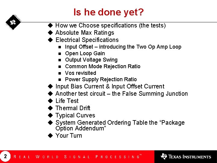
Is he done yet? u How we Choose specifications (the tests) u Absolute Max Ratings u Electrical Specifications n n n u u u Input Offset – introducing the Two Op Amp Loop Open Loop Gain Output Voltage Swing Common Mode Rejection Ratio Vos revisited Power Supply Rejection Ratio Input Bias Current & Input Offset Current Another test circuit – the False Summing Junction Life Test Thermal Drift Typical Curves System Generated Ordering Table the “Package Option Addendum” u Your Turn 2

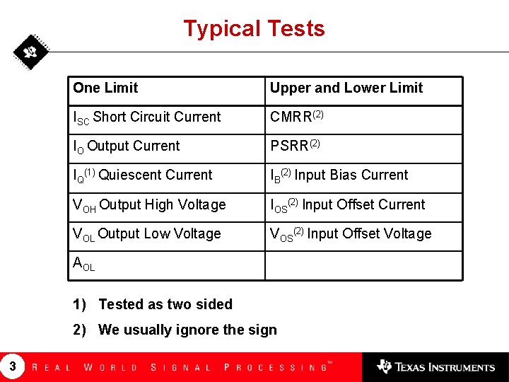
Typical Tests One Limit Upper and Lower Limit ISC Short Circuit Current CMRR(2) IO Output Current PSRR(2) IQ(1) Quiescent Current IB(2) Input Bias Current VOH Output High Voltage IOS(2) Input Offset Current VOL Output Low Voltage VOS(2) Input Offset Voltage AOL 1) Tested as two sided 2) We usually ignore the sign 3

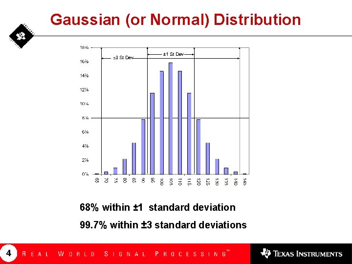
Gaussian (or Normal) Distribution 68% within ± 1 standard deviation 99. 7% within ± 3 standard deviations 4

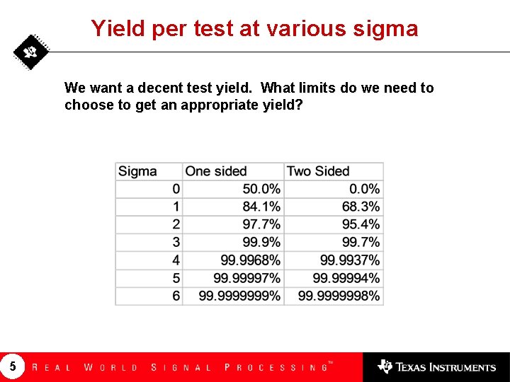
Yield per test at various sigma We want a decent test yield. What limits do we need to choose to get an appropriate yield? 5

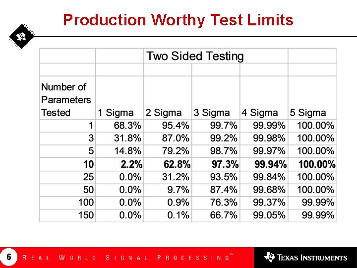
Production Worthy Test Limits 6

7

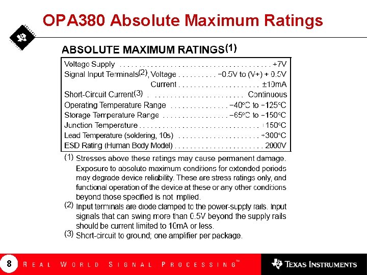
OPA 380 Absolute Maximum Ratings 8

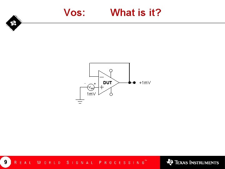
Vos: What is it? VOS + 1 m. V 9 DUT +1 m. V

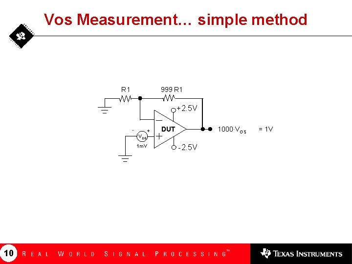
Vos Measurement… simple method R 1 999 R 1 +2. 5 V VOS 1 m. V 10 + DUT 1000·VOS -2. 5 V = 1 V

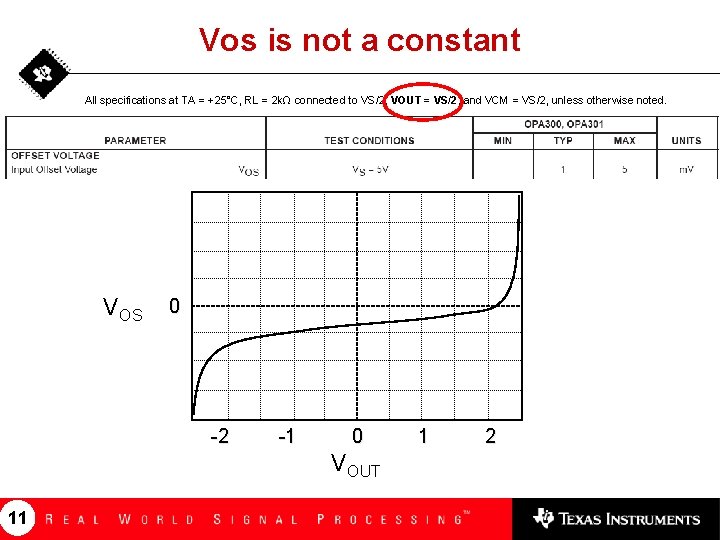
Vos is not a constant All specifications at TA = +25°C, RL = 2 kΩ connected to VS/2, VOUT = VS/2, and VCM = VS/2, unless otherwise noted. VOS 0 -2 -1 0 VOUT 11 1 2

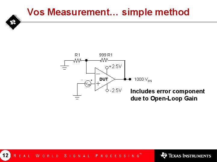
Vos Measurement… simple method R 1 999 R 1 +2. 5 V VOS + DUT 1000·VOS -2. 5 V 12 Includes error component due to Open-Loop Gain

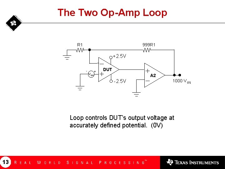
The Two Op-Amp Loop 999 R 1 +2. 5 V - VOS + DUT A 2 -2. 5 V 1000·VOS Loop controls DUT’s output voltage at accurately defined potential. (0 V) 13

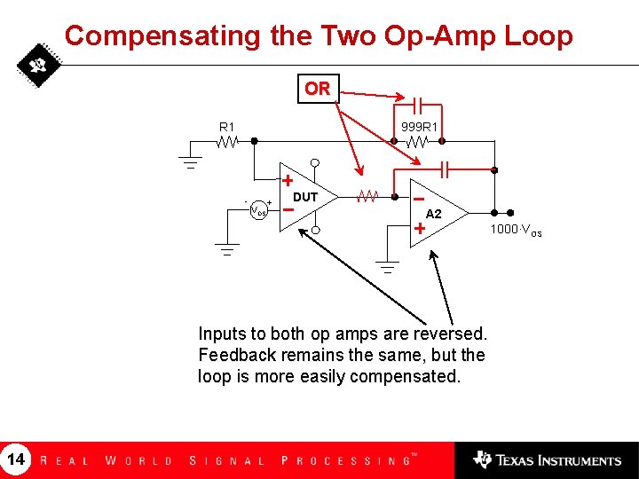
Compensating the Two Op-Amp Loop OR 999 R 1 - VOS + DUT A 2 1000·VOS Inputs to both op amps are reversed. Feedback remains the same, but the loop is more easily compensated. 14

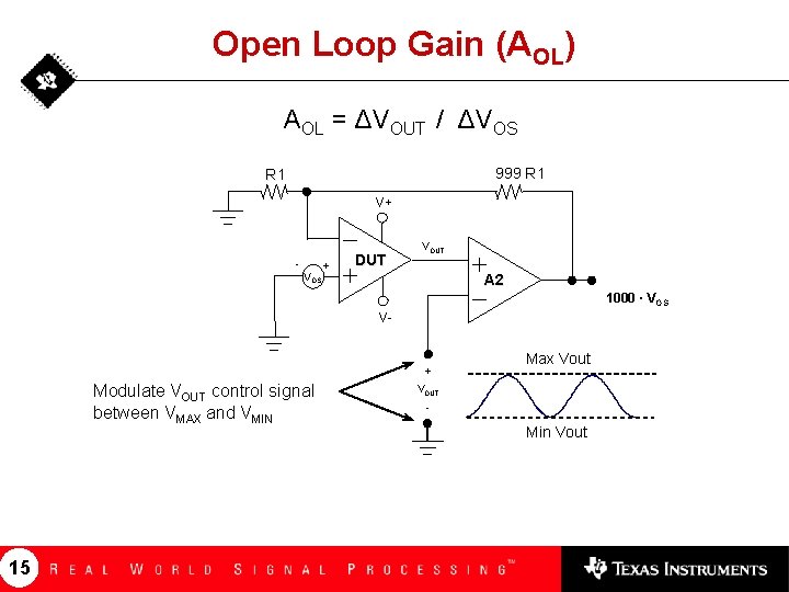
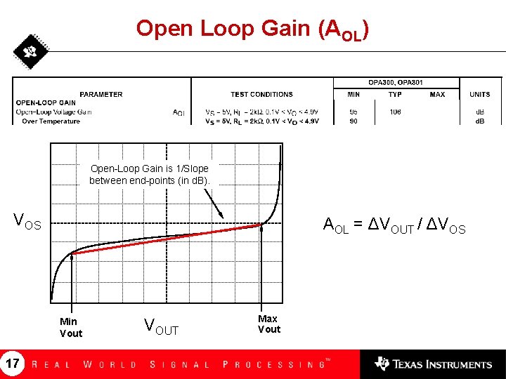
Open Loop Gain (AOL) AOL = ΔVOUT / ΔVOS 999 R 1 V+ - VOS + DUT VOUT A 2 1000 · VOS V- + Modulate VOUT control signal between VMAX and VMIN 15 Max Vout VOUT - Min Vout

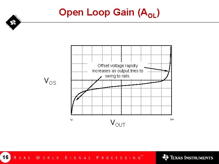
Open Loop Gain (AOL) Offset voltage rapidly increases as output tries to swing to rails. VOS V- 16 VOUT V+

Open Loop Gain (AOL) Open-Loop Gain is 1/Slope between end-points (in d. B). VOS AOL = ΔVOUT / ΔVOS Min Vout 17 VOUT Max Vout

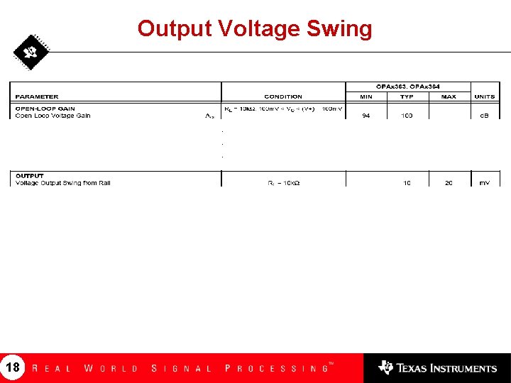
Output Voltage Swing . . . 18

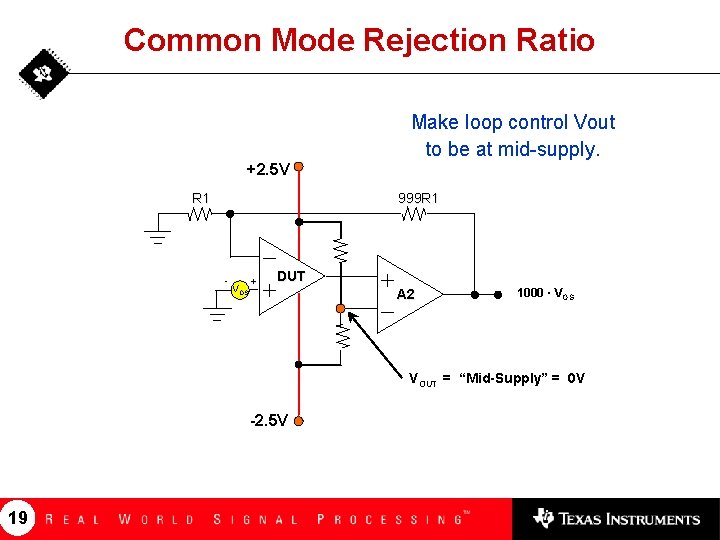
Common Mode Rejection Ratio Make loop control Vout to be at mid-supply. +2. 5 V R 1 999 R 1 - VOS + DUT A 2 1000 · VOS VOUT = “Mid-Supply” = 0 V -2. 5 V 19

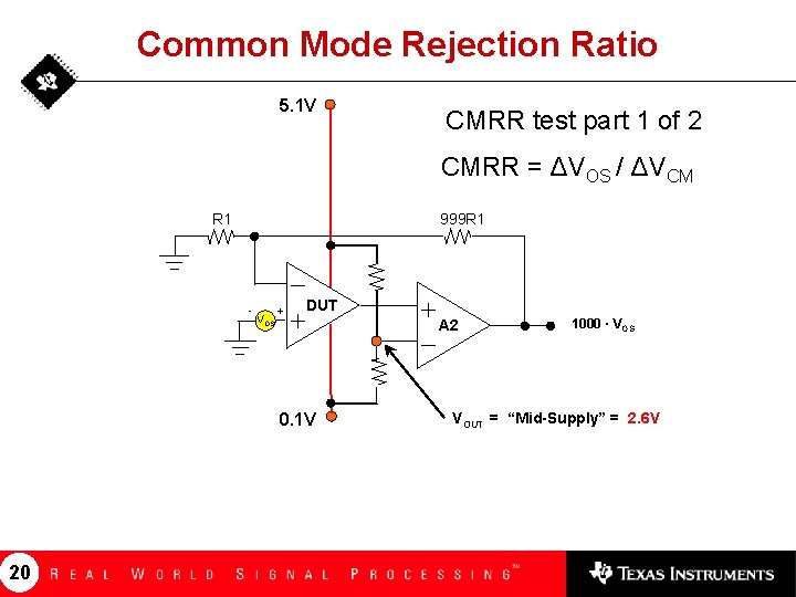
Common Mode Rejection Ratio 5. 1 V CMRR test part 1 of 2 CMRR = ΔVOS / ΔVCM R 1 999 R 1 - VOS + DUT 0. 1 V 20 A 2 1000 · VOS VOUT = “Mid-Supply” = 2. 6 V

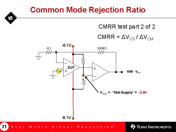
Common Mode Rejection Ratio CMRR test part 2 of 2 CMRR = ΔVOS / ΔVCM -0. 1 V R 1 - VOS + 999 R 1 DUT 1000 · VOS VOUT = “Mid-Supply” = -2. 6 V -5. 1 V 21

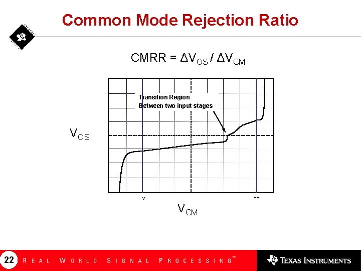
Common Mode Rejection Ratio CMRR = ΔVOS / ΔVCM Transition Region Between two input stages VOS V- 22 V+ VCM

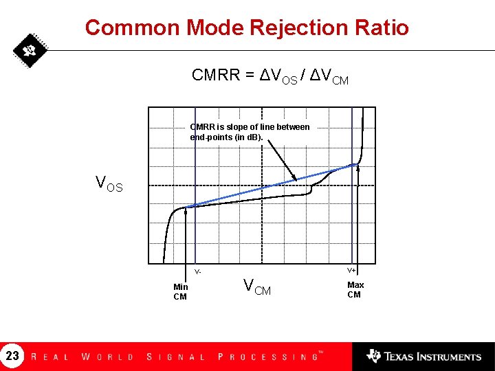
Common Mode Rejection Ratio CMRR = ΔVOS / ΔVCM CMRR is slope of line between end-points (in d. B). VOS V- Min CM 23 V+ VCM Max CM

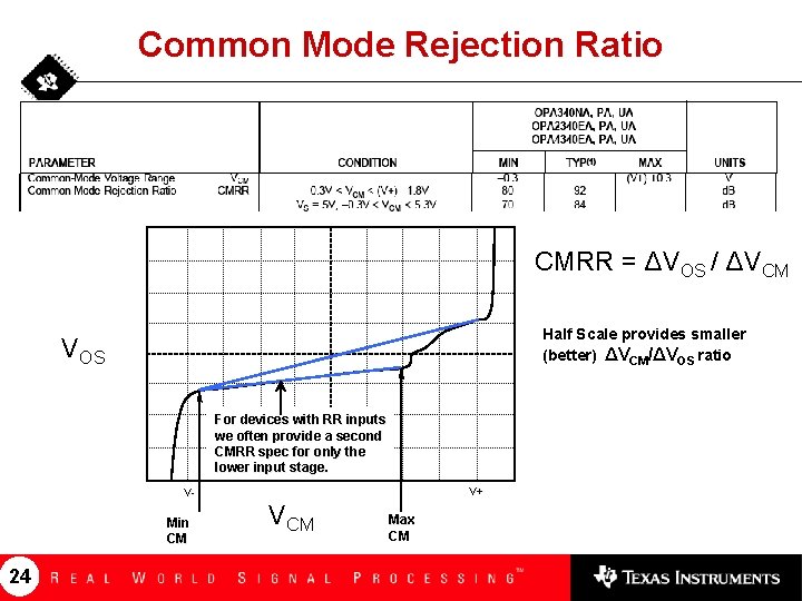
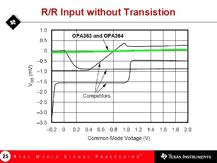
Common Mode Rejection Ratio CMRR = ΔVOS / ΔVCM Half Scale provides smaller (better) ΔVCM/ΔVOS ratio VOS For devices with RR inputs we often provide a second CMRR spec for only the lower input stage. V+ V- Min CM 24 VCM Max CM

R/R Input without Transistion 25

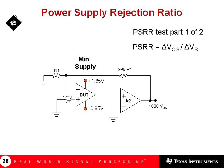
Power Supply Rejection Ratio PSRR test part 1 of 2 PSRR = ΔVOS / ΔVS Min Supply R 1 999 R 1 +1. 85 V - VOS + DUT A 2 -0. 85 V 26 1000·VOS

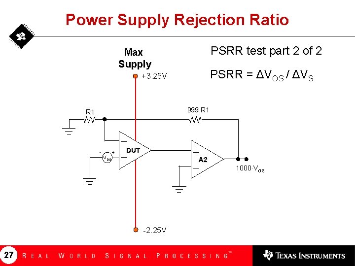
Power Supply Rejection Ratio PSRR test part 2 of 2 Max Supply PSRR = ΔVOS / ΔVS +3. 25 V 999 R 1 VOS + DUT A 2 1000·VOS -2. 25 V 27

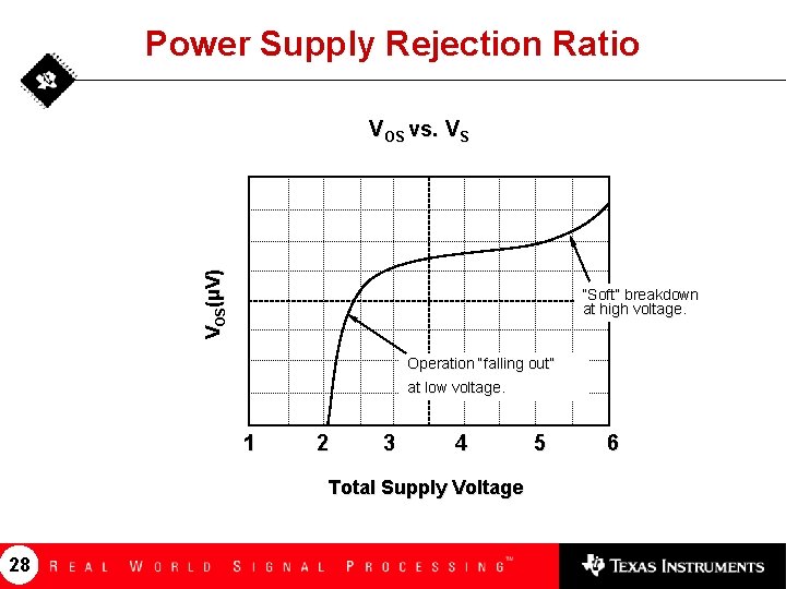
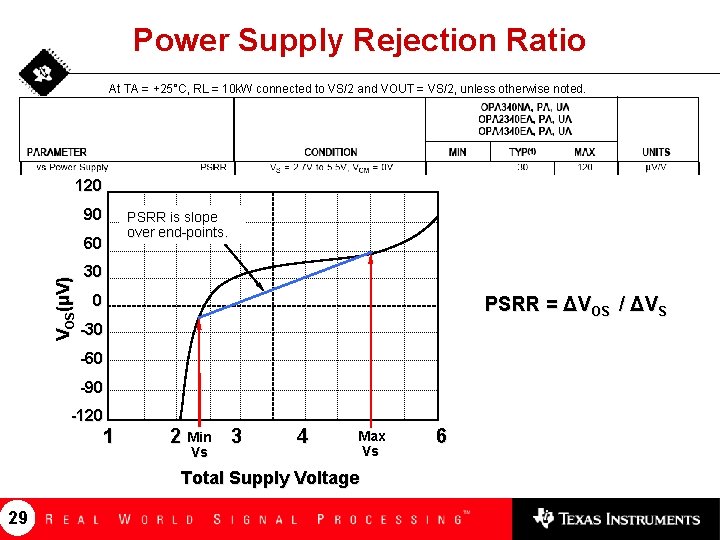
Power Supply Rejection Ratio VOS(μV) VOS vs. VS “Soft” breakdown at high voltage. Operation “falling out” at low voltage. 1 2 3 4 Total Supply Voltage 28 5 6

Power Supply Rejection Ratio At TA = +25°C, RL = 10 k. W connected to VS/2 and VOUT = VS/2, unless otherwise noted. 120 90 PSRR is slope over end-points. VOS(μV) 60 30 0 PSRR = ΔVOS / ΔVS -30 -60 -90 -120 1 2 Min 3 Vs 4 Max Vs Total Supply Voltage 29 6

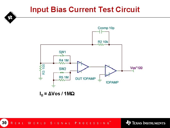
Input Bias Current Test Circuit IB = ΔVos / 1 M 30

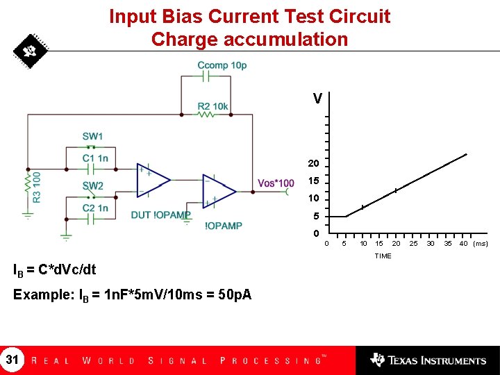
Input Bias Current Test Circuit Charge accumulation V 20 15 10 5 0 0 5 10 15 TIME IB = C*d. Vc/dt Example: IB = 1 n. F*5 m. V/10 ms = 50 p. A 31 20 25 30 35 40 (ms)

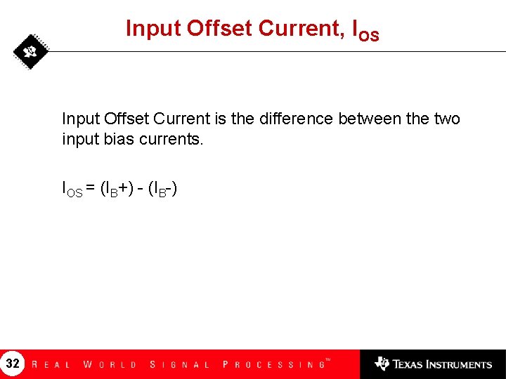
Input Offset Current, IOS Input Offset Current is the difference between the two input bias currents. IOS = (IB+) - (IB-) 32

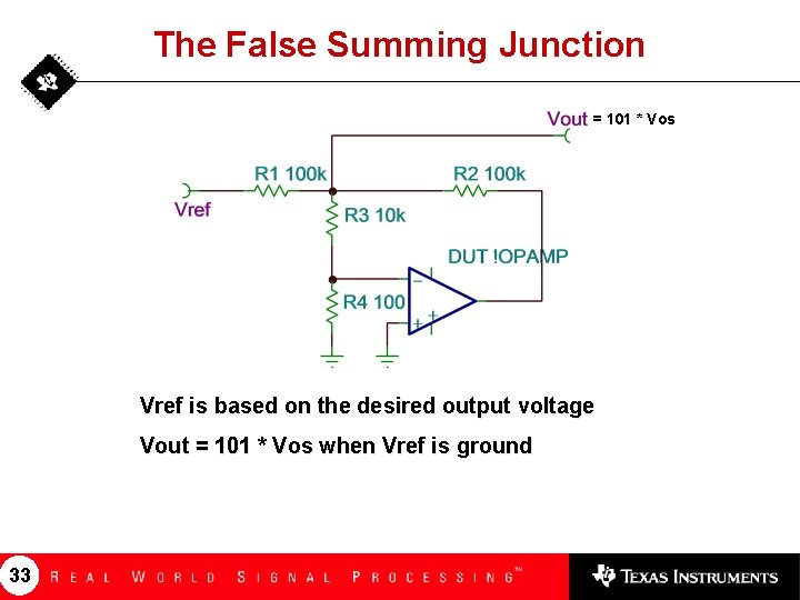
The False Summing Junction = 101 * Vos Vref is based on the desired output voltage Vout = 101 * Vos when Vref is ground 33

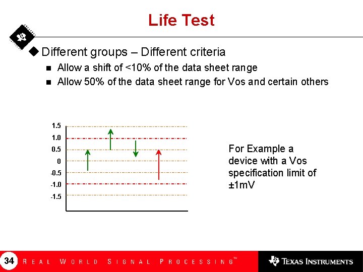
Life Test u Different groups – Different criteria n n Allow a shift of <10% of the data sheet range Allow 50% of the data sheet range for Vos and certain others 1. 5 1. 0 0. 5 0 -0. 5 -1. 0 -1. 5 34 For Example a device with a Vos specification limit of ± 1 m. V

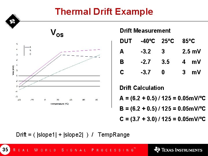
Thermal Drift Example VOS Drift Measurement DUT -40ºC 25ºC 85ºC A -3. 2 3 2. 5 m. V B -2. 7 3. 5 4 m. V C -3. 7 0 3 m. V Drift Calculation A = (6. 2 + 0. 5) / 125 = 0. 05 m. V/ºC B = (6. 2 + 0. 5) / 125 = 0. 05 m. V/ºC C = (3. 7 + 3. 0) / 125 = 0. 05 m. V/ºC Drift = ( |slope 1| + |slope 2| ) / Temp. Range 35

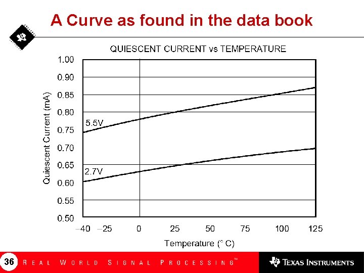
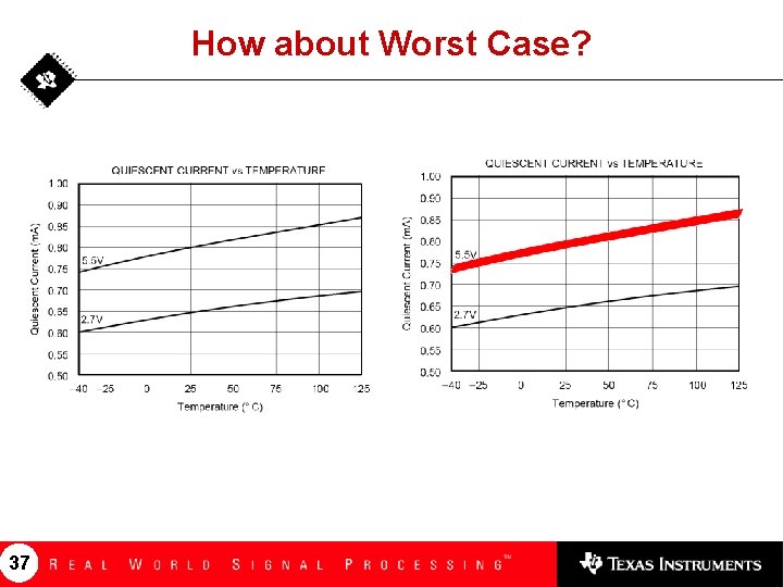
A Curve as found in the data book 36

How about Worst Case? 37

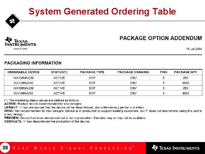
System Generated Ordering Table 38

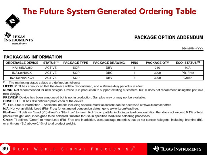
The Future System Generated Ordering Table 39

The End Your Turn to talk 40