OnModule Interconnection and CNM Projects No thinning in
- Slides: 15

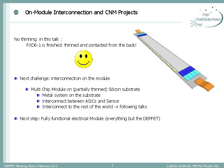
On-Module Interconnection and CNM Projects No thinning in this talk : PXD 6 -1 is finished: thinned and contacted from the§ back! update on thinning samples for thermal mock-ups preparations for PXD 6 thinning § on module interconnection (3 rd metal layer) CNM Project Cu Process at HLL Next challenge: interconnection on the module Multi Chip Module on (partially thinned) Silicon substrate Metal system on the substrate interconnect between ASICs and Sensor Interconnect to the rest of the world following talks Next step: Fully functional electrical Module (everything but the DEPFET) DEPFET Meeting, Bonn, February 2011 1 Ladislav Andricek, MPI für Physik, HLL

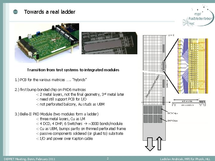
Towards a real ladder Transition from test systems to integrated modules 1. ) PCB for the various matrices …. . “hybrids” 2. ) first bump bonded chip on PXD 6 matrices -: 2 metal layers, not the final geometry, 3 rd metal later -: need still support PCB for I/O -: not perforated balcony, Au studs as UBM 3. ) Belle-II PXD Module (two modules form a ladder) -: three metal layers, Cu as LM -: 4 DCD, 4 DHP, 6 Switchers ~3000 bonds/module -: Cu as UBM, bumps partly on thinned perforated frame -: passive components soldered (or glued to) substrate -: I/O and power over Kapton cable DEPFET Meeting, Bonn, February 2011 2 Ladislav Andricek, MPI für Physik, HLL

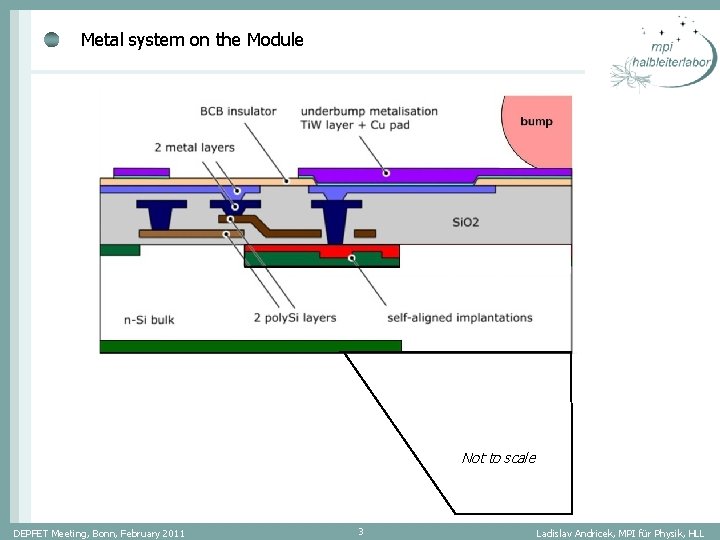
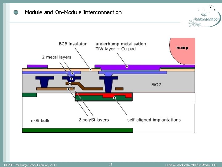
Metal system on the Module § update on thinning samples for thermal mock-ups preparations for PXD 6 thinning § on module interconnection (3 rd metal layer) CNM Project Cu Process at HLL Not to scale DEPFET Meeting, Bonn, February 2011 3 Ladislav Andricek, MPI für Physik, HLL

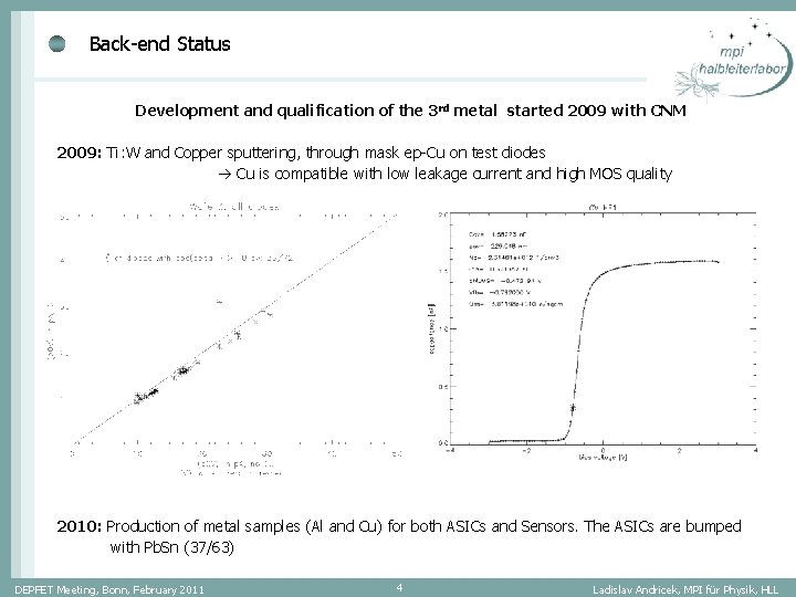
Back-end Status Development and qualification of the 3 rd metal started 2009 with CNM 2009: Ti: W and Copper sputtering, through mask ep-Cu on test diodes § update on thinning Cu is compatible with low leakage current and high MOS quality samples for thermal mock-ups preparations for PXD 6 thinning § on module interconnection (3 rd metal layer) CNM Project Cu Process at HLL 2010: Production of metal samples (Al and Cu) for both ASICs and Sensors. The ASICs are bumped with Pb. Sn (37/63) DEPFET Meeting, Bonn, February 2011 4 Ladislav Andricek, MPI für Physik, HLL

CNM Project 2010 -: project is divided in three parts: I. provide “sensor” samples with two metal layers (Al and Cu) II. ASIC dummies (DCDB and Switcher. B) with eutectic Pb. Sn bumps III. Bump bonding of ASIC dummies to “Sensor” -: work sharing: HLL: mask design provide passivated Al samples of both, the Sensor and the ASIC wafers on std. material CNM: Cu electro-plating of the sensor wafer bumping of the ASIC wafer dicing of the wafers and bump bonding of the ASCIs to the sensor substrate -: time line: finish in the first quarter of 2011 DEPFET Meeting, Bonn, February 2011 5 Ladislav Andricek, MPI für Physik, HLL

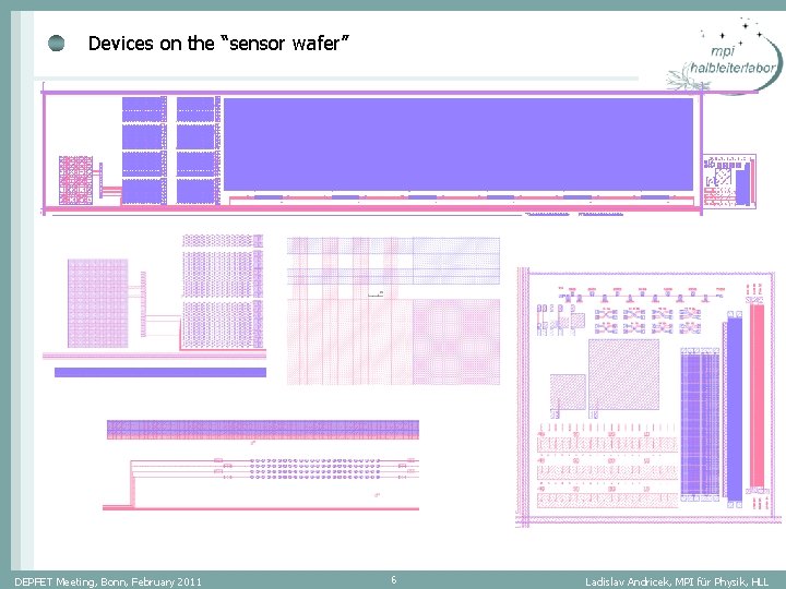
Devices on the “sensor wafer” DEPFET Meeting, Bonn, February 2011 6 Ladislav Andricek, MPI für Physik, HLL

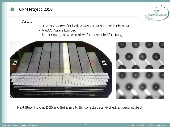
CNM Project 2010 Status: -: 4 Sensor wafers finished, 2 with Cu LM and 2 with Pb. Sn LM -: 6 ASIC Wafers bumped -: latest news (last week): all wafers scheduled for dicing Next Step: flip chip DCD and Switchers to Sensor substrate check procedure, yield … DEPFET Meeting, Bonn, February 2011 7 Ladislav Andricek, MPI für Physik, HLL

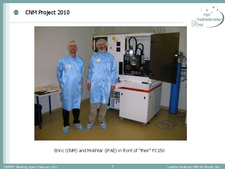
CNM Project 2010 Enric (CNM) and Mokhtar (IFAE) in front of “their” FC 150 DEPFET Meeting, Bonn, February 2011 8 Ladislav Andricek, MPI für Physik, HLL

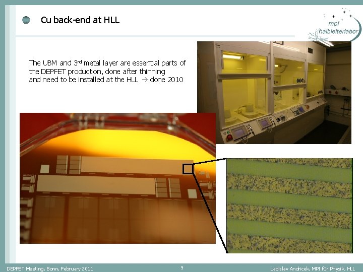
Cu back-end at HLL The UBM and 3 rd metal layer are essential parts of the DEPFET production, done after thinning and need to be installed at the HLL done 2010 DEPFET Meeting, Bonn, February 2011 9 Ladislav Andricek, MPI für Physik, HLL

Intermediate summary -: the Cu metal system (BCB – Ti: W – Cu) seems to be compatible with our process -: more tests concerning the BCB isolator will be done on the next Cu-wafers produced at the HLL. -: CNM produced bumped ASIC dummies an is looking forward to bump bonding these chips to sensor dummies. This will give us hopefully the answer to the question, whether we can really solder reliably to Cu pads. We could also practice the attachment of Hans’ kapton test samples to these modules. We are ready to do the next step: design and assembly of an electrically functional module (half ladder) DEPFET Meeting, Bonn, February 2011 10 Ladislav Andricek, MPI für Physik, HLL

The plan … just a starting point… -: The goal is to build the first fully functional MCM on Silicon everything but the DEPFET -: -: 3 Metal system with the ILD as close as possible to the final module ASICs: Switcher. B, DCDB, DHP 0. 2 Off-Module interconnect as close as possible to final (Kapton. . ) place all necessary passives -: Geometry: outer layer module, 106 -011113. idw with wide kapton layout need at least one iteration between electrical, mechanical and thermal WG to define the exact geometry -: the sensitive region will be free for test structures , bypass pads, test pads for the swticher channels, load capacitors and resistors even as space for a pxd 6 matrix. First brain storming meeting was held in December in Mannheim with participants from Mannheim, Bonn, and Munich (LMU and MPI) and the outcome is placed as a working document on our wiki pages. DEPFET Meeting, Bonn, February 2011 11 Ladislav Andricek, MPI für Physik, HLL

Actions (very rough…) 1. Draw schematic and first layout in consultation with the chip designers: Uni Heidelberg 2. Re-iterate with mechanical and thermal WG 3. Design test structures and schemes for the “sensitive region”: HLL, Heidelberg, Bonn 3. Schedule double-metal run at HLL, prepare Cu layer deposition: HLL 4. Prepare the ASICs (bumping etc…): Bonn, Heidelberg is there a way to get bumped IBM and UMC Dummies? 5. Prepare and qualify bumping: CNM 6. Assembly at CNM DEPFET Meeting, Bonn, February 2011 12 Ladislav Andricek, MPI für Physik, HLL

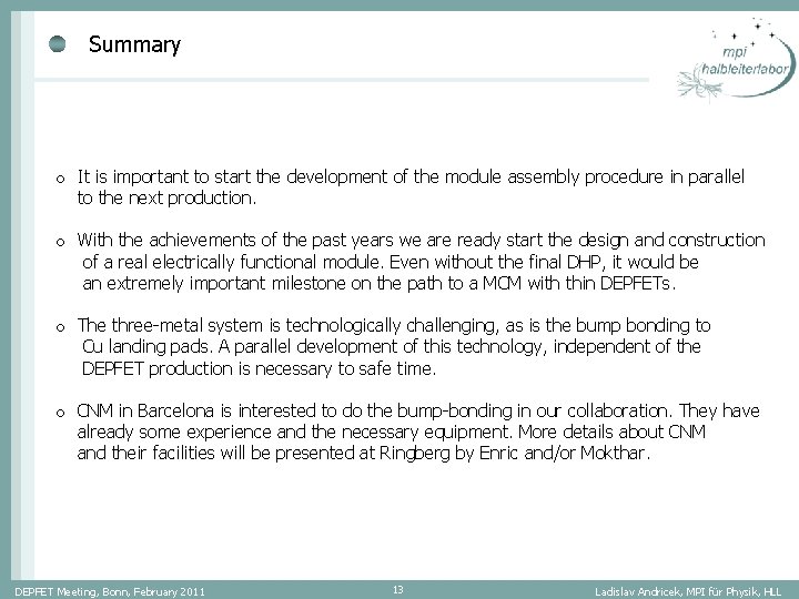
Summary o It is important to start the development of the module assembly procedure in parallel to the next production. o With the achievements of the past years we are ready start the design and construction of a real electrically functional module. Even without the final DHP, it would be an extremely important milestone on the path to a MCM with thin DEPFETs. o The three-metal system is technologically challenging, as is the bump bonding to Cu landing pads. A parallel development of this technology, independent of the DEPFET production is necessary to safe time. o CNM in Barcelona is interested to do the bump-bonding in our collaboration. They have already some experience and the necessary equipment. More details about CNM and their facilities will be presented at Ringberg by Enric and/or Mokthar. DEPFET Meeting, Bonn, February 2011 13 Ladislav Andricek, MPI für Physik, HLL

Backup slides follow DEPFET Meeting, Bonn, February 2011 14 Ladislav Andricek, MPI für Physik, HLL

Module and On-Module Interconnection bump DEPFET Meeting, Bonn, February 2011 15 Ladislav Andricek, MPI für Physik, HLL