On the development of the final optical multiplexer


- Slides: 21

On the development of the final optical multiplexer board prototype for the Tile. Cal experiment V. González Dep. of Electronic Engineering University of Valencia, Spain

Outline Introduction Previous work OMB 6 U Final prototype OMB 9 U Present status

Introduction RODs interface LVL 1 and LVL 2 at each detector – Some preprocessing available if needed For Tile. Cal, radiation issues changed front end connection to RODs – Two fibers with same data output each Front. End board – Need to select the fiber with good data in case of errors (OMB aka Pre. ROD)

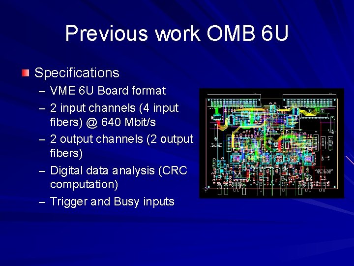
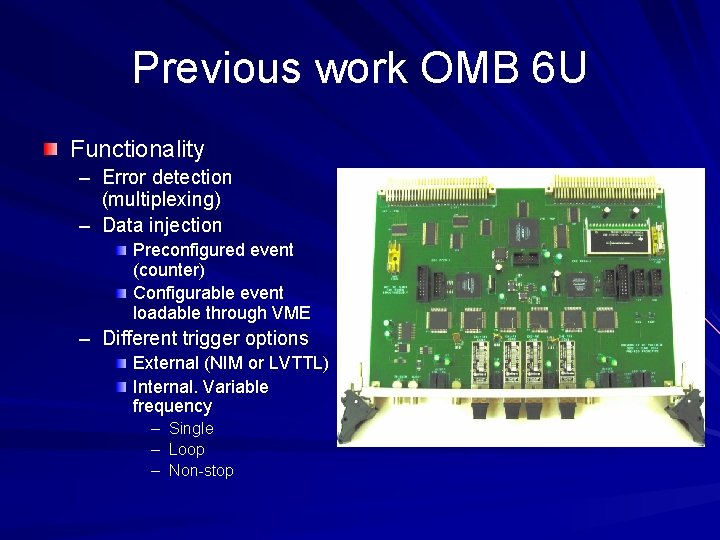
Previous work OMB 6 U Specifications – VME 6 U Board format – 2 input channels (4 input fibers) @ 640 Mbit/s – 2 output channels (2 output fibers) – Digital data analysis (CRC computation) – Trigger and Busy inputs

Previous work OMB 6 U Functionality – Error detection (multiplexing) – Data injection Preconfigured event (counter) Configurable event loadable through VME – Different trigger options External (NIM or LVTTL) Internal. Variable frequency – – – Single Loop Non-stop

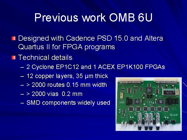
Previous work OMB 6 U Designed with Cadence PSD 15. 0 and Altera Quartus II for FPGA programs Technical details – – – 2 Cyclone EP 1 C 12 and 1 ACEX EP 1 K 100 FPGAs 12 copper layers, 35 μm thick > 2000 routes 0. 15 mm width > 2000 vias 0. 2 mm SMD components widely used

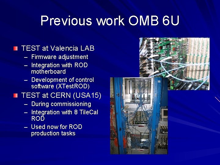
Previous work OMB 6 U TEST at Valencia LAB – Firmware adjustment – Integration with ROD motherboard – Development of control software (XTest. ROD) TEST at CERN (USA 15) – During commissioning – Integration with 8 Tile. Cal ROD – Used now for ROD production tasks

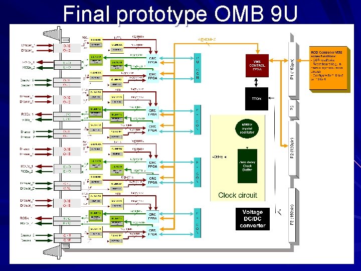
Final prototype OMB 9 U Same basic functionality – CRC checking – Data injection – 40 MHz clock Differences – 8 channels 16 input fibers 8 output fibers – TTCrx – Mezzanine connectors: more processing power?

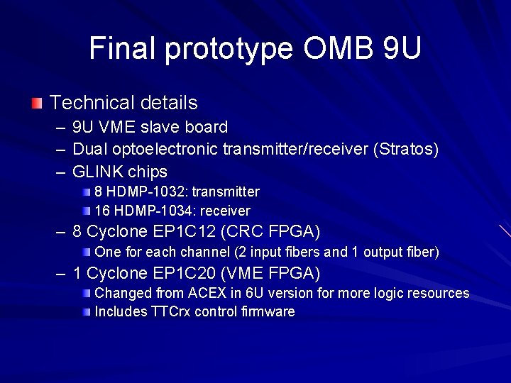
Final prototype OMB 9 U Technical details – 9 U VME slave board – Dual optoelectronic transmitter/receiver (Stratos) – GLINK chips 8 HDMP-1032: transmitter 16 HDMP-1034: receiver – 8 Cyclone EP 1 C 12 (CRC FPGA) One for each channel (2 input fibers and 1 output fiber) – 1 Cyclone EP 1 C 20 (VME FPGA) Changed from ACEX in 6 U version for more logic resources Includes TTCrx control firmware

Final prototype OMB 9 U

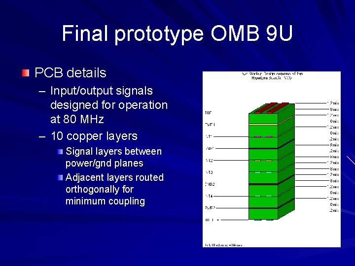
Final prototype OMB 9 U PCB details – Input/output signals designed for operation at 80 MHz – 10 copper layers Signal layers between power/gnd planes Adjacent layers routed orthogonally for minimum coupling

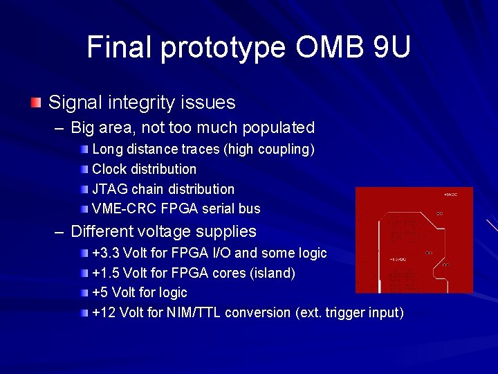
Final prototype OMB 9 U Signal integrity issues – Big area, not too much populated Long distance traces (high coupling) Clock distribution JTAG chain distribution VME-CRC FPGA serial bus – Different voltage supplies +3. 3 Volt for FPGA I/O and some logic +1. 5 Volt for FPGA cores (island) +5 Volt for logic +12 Volt for NIM/TTL conversion (ext. trigger input)

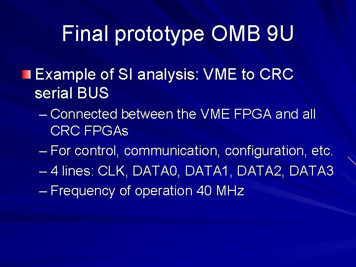
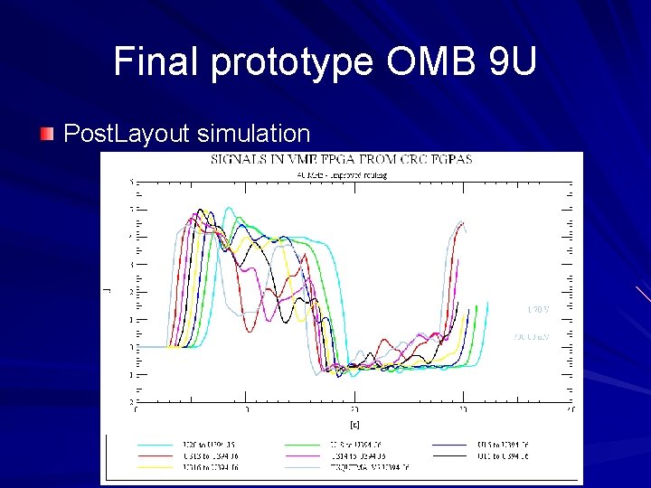
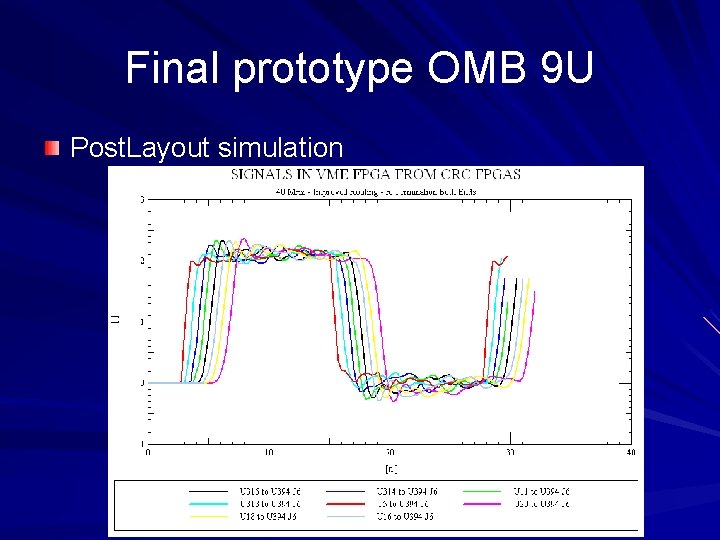
Final prototype OMB 9 U Example of SI analysis: VME to CRC serial BUS – Connected between the VME FPGA and all CRC FPGAs – For control, communication, configuration, etc. – 4 lines: CLK, DATA 0, DATA 1, DATA 2, DATA 3 – Frequency of operation 40 MHz

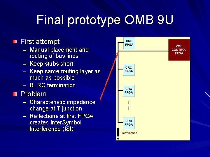
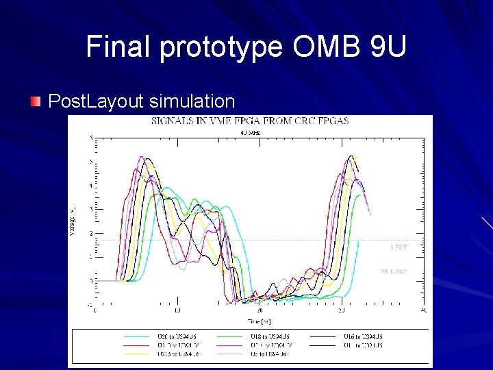
Final prototype OMB 9 U First attempt – Manual placement and routing of bus lines – Keep stubs short – Keep same routing layer as much as possible – R, RC termination Problem – Characteristic impedance change at T junction – Reflections at first FPGA creates Inter. Symbol Interference (ISI)

Final prototype OMB 9 U Post. Layout simulation

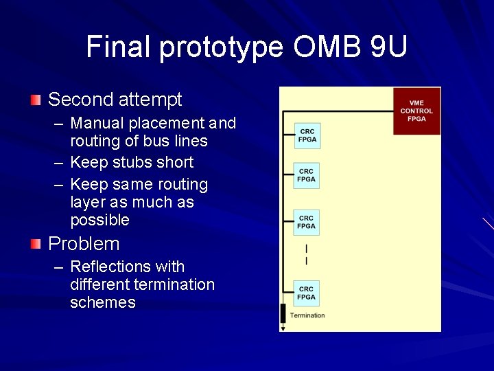
Final prototype OMB 9 U Second attempt – Manual placement and routing of bus lines – Keep stubs short – Keep same routing layer as much as possible Problem – Reflections with different termination schemes

Final prototype OMB 9 U Post. Layout simulation

Final prototype OMB 9 U Final attempt – Manual placement and routing of bus lines – Keep stubs short – Keep same routing layer as much as possible Solution – Resistive termination at both ends

Final prototype OMB 9 U Post. Layout simulation

Present status Stratos change connectors to be Ro. HS compliant – Need to test new connectors Board routing on the way – SI analysis still undergoing: JTAG chain, clock distribution and power distribution FPGA firmware adaptation

THANK YOU FOR YOUR ATTENTION