On Effective IDDQ Testing of LowVoltage CMOS Circuits
![Problem statement Earlier Technologies[5] For new Technologies (Deep submicron levels) Low threshold Transistors Higher Problem statement Earlier Technologies[5] For new Technologies (Deep submicron levels) Low threshold Transistors Higher](https://slidetodoc.com/presentation_image_h2/d13a31bbc076c9d129d97bef68b32f12/image-4.jpg)

![Papers [1] Chen, Zhanping, Liqiong Wei, and Kaushik Roy. "On effective I/sub DDQ/testing of Papers [1] Chen, Zhanping, Liqiong Wei, and Kaushik Roy. "On effective I/sub DDQ/testing of](https://slidetodoc.com/presentation_image_h2/d13a31bbc076c9d129d97bef68b32f12/image-22.jpg)
![Paper Map [5] Final model for effective IDDQ test Assigning different vectors to reduce Paper Map [5] Final model for effective IDDQ test Assigning different vectors to reduce](https://slidetodoc.com/presentation_image_h2/d13a31bbc076c9d129d97bef68b32f12/image-23.jpg)
- Slides: 23

On Effective IDDQ Testing of Low-Voltage CMOS Circuits Using Leakage Control Techniques st Robu Low ECE er Pow 7502 LSI V S 2015 ECE 7502 Class Discussion W. P. M. R Pathirana 31 st March 2015

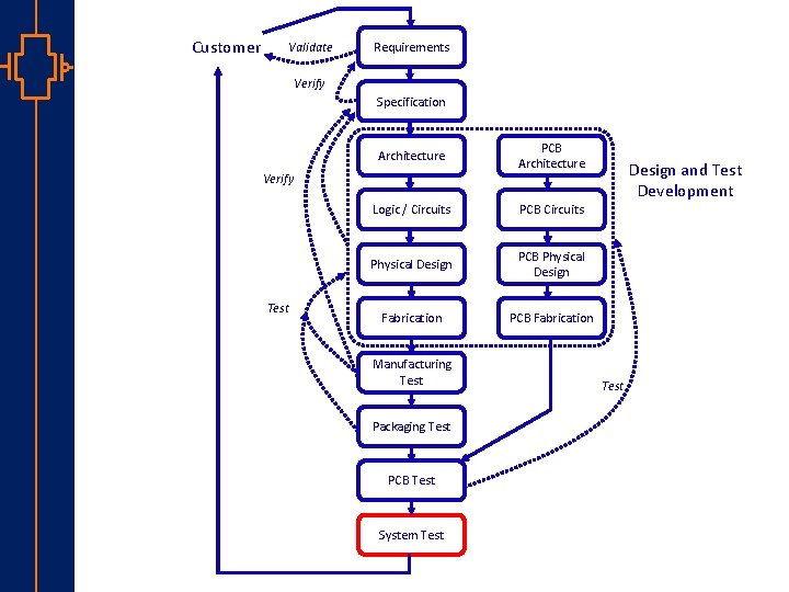
Customer Validate Requirements Verify Specification Architecture PCB Architecture Logic / Circuits PCB Circuits Physical Design PCB Physical Design Fabrication PCB Fabrication Verify Test Manufacturing Test Packaging Test st Robu Low er Pow VLSI PCB Test System Test Design and Test Development Test

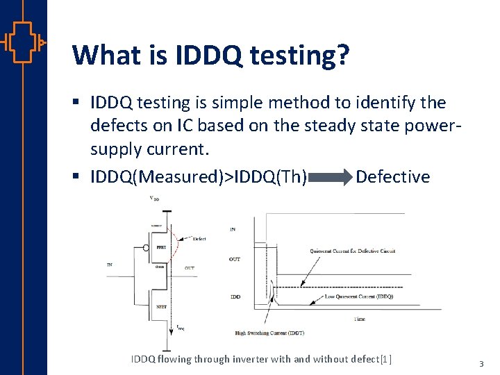
What is IDDQ testing? § IDDQ testing is simple method to identify the defects on IC based on the steady state powersupply current. § IDDQ(Measured)>IDDQ(Th) Defective st Robu Low er Pow VLSI IDDQ flowing through inverter with and without defect[1] 3
![Problem statement Earlier Technologies5 For new Technologies Deep submicron levels Low threshold Transistors Higher Problem statement Earlier Technologies[5] For new Technologies (Deep submicron levels) Low threshold Transistors Higher](https://slidetodoc.com/presentation_image_h2/d13a31bbc076c9d129d97bef68b32f12/image-4.jpg)
Problem statement Earlier Technologies[5] For new Technologies (Deep submicron levels) Low threshold Transistors Higher Leakage Deep submicron Technologies[5] IDDQ(Fault Free)≈IDDQ(Defective) st Robu Low er Pow VLSI Test escapes and yield loss A-test escapes B-yield loss 4

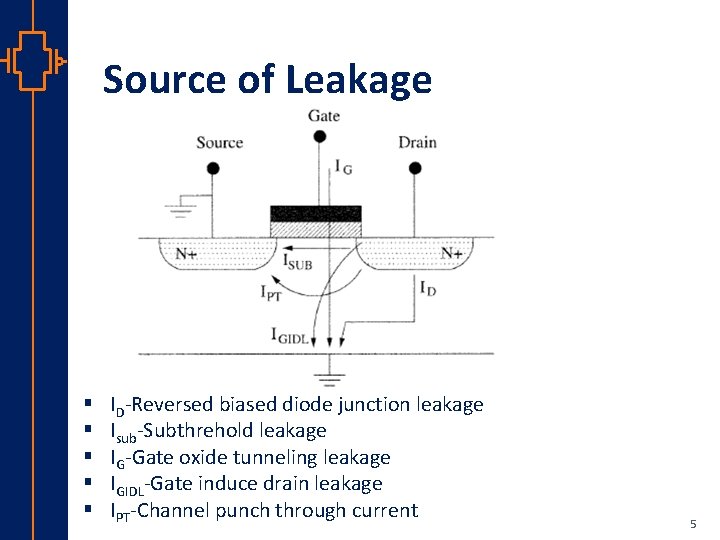
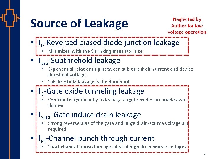
Source of Leakage st Robu Low er Pow VLSI § § § ID-Reversed biased diode junction leakage Isub-Subthrehold leakage IG-Gate oxide tunneling leakage IGIDL-Gate induce drain leakage IPT-Channel punch through current 5

Source of Leakage Neglected by Author for low voltage operation § ID-Reversed biased diode junction leakage § Minimized with the Shrinking transistor size § Isub-Subthrehold leakage § Exponential relationship between sub threshold current and device threshold voltage § Subthreshold leakage is the dominant § IG-Gate oxide tunneling leakage § Contribute significantly to leakage as gate oxides are made ever thinner § IGIDL-Gate induce drain leakage st Robu Low er Pow VLSI § Strong reverse bias of the gate and large drain-source voltage are required § IPT-Channel punch through current § Short channel transistors operated at high drain source voltages 6

Leakage current model § γ'-Linearized body effect coefficient § If Vs is small, body effect is linear and represent with γ’Vs st Robu Low er Pow VLSI § η-DIBL coefficient § μ 0 -Zero bias mobility § n-Subthrehold swing coefficient § n = 1+ ξsitox/ξoxtsi § ξ-permittivity and t-thickness of the depletion layer 7

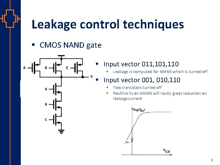
Leakage control techniques § CMOS NAND gate § Input vector 011, 101, 110 § Leakage is computed for NMOS which is turned off § Input vector 001, 010, 110 § Two transistors turned off § Positive Vs on NMOS will reults great reduction on leakage current st Robu Low er Pow VLSI 8

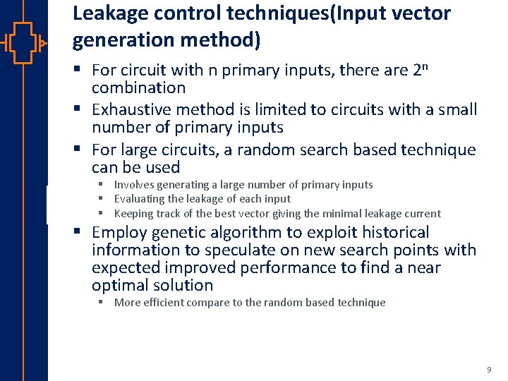
Leakage control techniques(Input vector generation method) § For circuit with n primary inputs, there are 2 n combination § Exhaustive method is limited to circuits with a small number of primary inputs § For large circuits, a random search based technique can be used § Involves generating a large number of primary inputs § Evaluating the leakage of each input § Keeping track of the best vector giving the minimal leakage current st Robu Low er Pow VLSI § Employ genetic algorithm to exploit historical information to speculate on new search points with expected improved performance to find a near optimal solution § More efficient compare to the random based technique 9

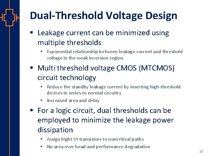
Dual-Threshold Voltage Design § Leakage current can be minimized using multiple thresholds § Exponential relationship between leakage current and threshold voltage in the weak inversion region § Multi threshold voltage CMOS (MTCMOS) circuit technology § Reduce the standby leakage current by inserting high-threshold devices in series to normal circuitry § Increased area and delay st Robu Low er Pow VLSI § For a logic circuit, dual thresholds can be employed to minimize the leakage power dissipation § Assign hight Vt transistors to noncritical paths § No area over head and performance degradation 10

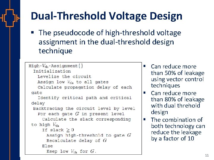
Dual-Threshold Voltage Design § The pseudocode of high-threshold voltage assignment in the dual-threshold design technique st Robu Low er Pow VLSI § Can reduce more than 50% of leakage using vector control techniques § Can reduce more than 80% of leakage with dual threhold design § The combination of both technology can reduce the leakage by a factor of 10 11

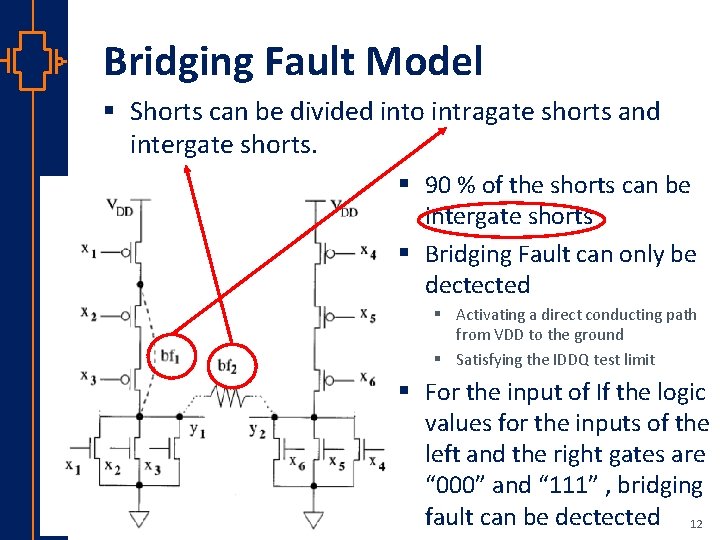
Bridging Fault Model § Shorts can be divided into intragate shorts and intergate shorts. § 90 % of the shorts can be intergate shorts § Bridging Fault can only be dectected § Activating a direct conducting path from VDD to the ground § Satisfying the IDDQ test limit st Robu Low er Pow VLSI § For the input of If the logic values for the inputs of the left and the right gates are “ 000” and “ 111” , bridging fault can be dectected 12

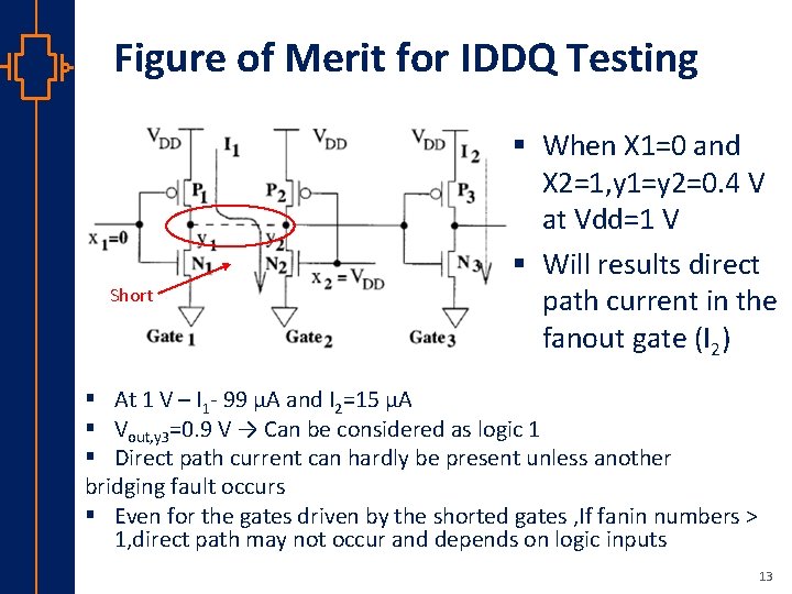
Figure of Merit for IDDQ Testing Short § When X 1=0 and X 2=1, y 1=y 2=0. 4 V at Vdd=1 V § Will results direct path current in the fanout gate (I 2) § At 1 V – I 1 - 99 μA and I 2=15 μA § Vout, y 3=0. 9 V → Can be considered as logic 1 § Direct path current can hardly be present unless another t s u b Ro bridging fault occurs Low er § Even for the gates driven by the shorted gates , If fanin numbers > Pow 1, direct path may not occur and depends on logic inputs VLSI 13

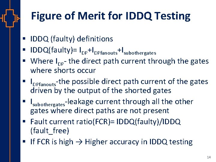
Figure of Merit for IDDQ Testing st Robu Low er Pow VLSI § IDDQ (faulty) definitions § IDDQ(faulty)= IDP+IDPfanouts+Isubothergates § Where IDP- the direct path current through the gates where shorts occur § IDPfanouts-the possible direct path current of the gates driven by the output of the shorted gates § Isubothergates-leakage current through all the other gates where direct paths are not present § Fault current ratio(FCR)= IDDQ(faulty)/IDDQ (fault_free) § If FCR is high → Higher accuracy in IDDQ testing 14

Implementation and experimental results § § Fault resistance value set to Zero ? ? ? 20 bridging faults are randomly introduced 20 test vectors are randomly generated Calculate the § FCRs-(Base line for comparison)-fault current ratio with a single low threshold § FCRd-dual-threshold voltage technique fault current ratio § FCRdv-dual-threshold voltage and vector control technique fault current ratio st Robu Low er Pow VLSI § Random search technique is used and select 20 out of 1000 vectors for FCRdv § FCRdv > FCRd>FCRs 15

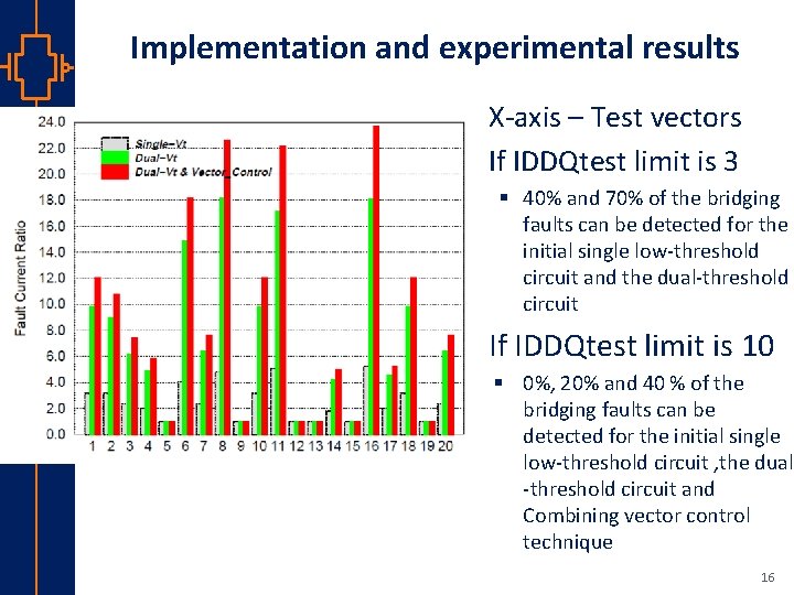
Implementation and experimental results § X-axis – Test vectors § If IDDQtest limit is 3 § 40% and 70% of the bridging faults can be detected for the initial single low-threshold circuit and the dual-threshold circuit § If IDDQtest limit is 10 st Robu Low er Pow VLSI § 0%, 20% and 40 % of the bridging faults can be detected for the initial single low-threshold circuit , the dual -threshold circuit and Combining vector control technique 16

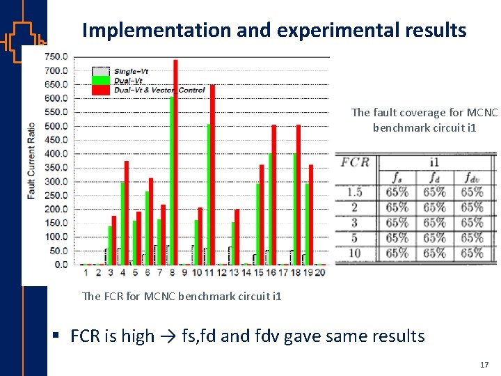
Implementation and experimental results The fault coverage for MCNC benchmark circuit i 1 st Robu Low er Pow VLSI The FCR for MCNC benchmark circuit i 1 § FCR is high → fs, fd and fdv gave same results 17

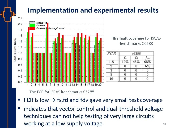
Implementation and experimental results The fault coverage for ISCAS benchmarks C 6288 The FCR for ISCAS benchmarks C 6288 st Robu Low er Pow VLSI § FCR is low → fs, fd and fdv gave very small test coverage § indicates that vector control and dual-threshold voltage techniques can not help testing of very large circuits 18 working at a low supply voltage

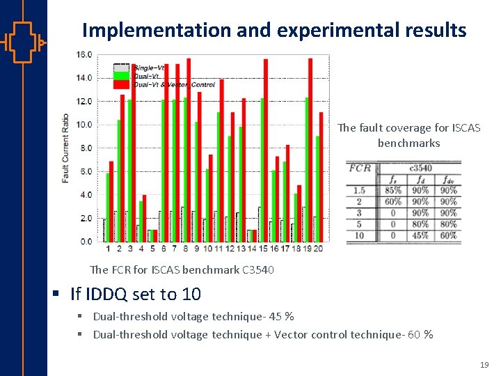
Implementation and experimental results The fault coverage for ISCAS benchmarks The FCR for ISCAS benchmark C 3540 st Robu Low er Pow VLSI § If IDDQ set to 10 § Dual-threshold voltage technique- 45 % § Dual-threshold voltage technique + Vector control technique- 60 % 19

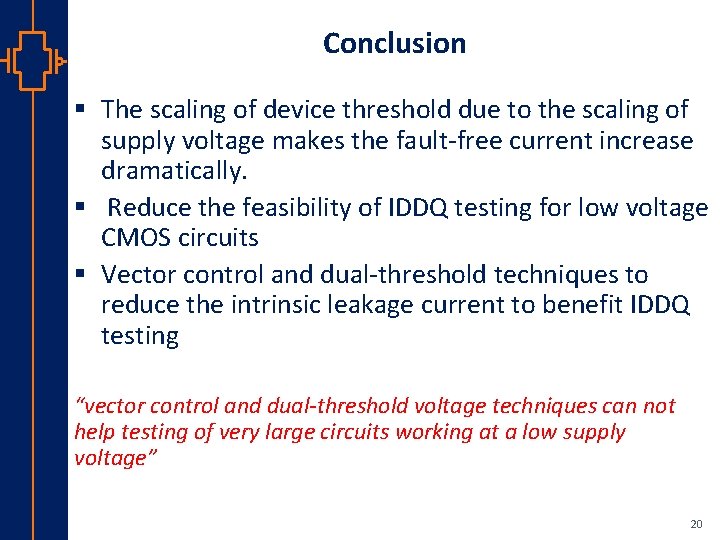
Conclusion § The scaling of device threshold due to the scaling of supply voltage makes the fault-free current increase dramatically. § Reduce the feasibility of IDDQ testing for low voltage CMOS circuits § Vector control and dual-threshold techniques to reduce the intrinsic leakage current to benefit IDDQ testing st Robu Low er Pow VLSI “vector control and dual-threshold voltage techniques can not help testing of very large circuits working at a low supply voltage” 20

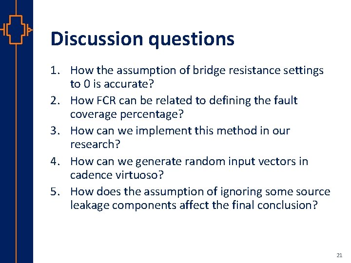
Discussion questions st Robu Low er Pow VLSI 1. How the assumption of bridge resistance settings to 0 is accurate? 2. How FCR can be related to defining the fault coverage percentage? 3. How can we implement this method in our research? 4. How can we generate random input vectors in cadence virtuoso? 5. How does the assumption of ignoring some source leakage components affect the final conclusion? 21
![Papers 1 Chen Zhanping Liqiong Wei and Kaushik Roy On effective Isub DDQtesting of Papers [1] Chen, Zhanping, Liqiong Wei, and Kaushik Roy. "On effective I/sub DDQ/testing of](https://slidetodoc.com/presentation_image_h2/d13a31bbc076c9d129d97bef68b32f12/image-22.jpg)
Papers [1] Chen, Zhanping, Liqiong Wei, and Kaushik Roy. "On effective I/sub DDQ/testing of lowvoltage CMOS circuits using leakage control techniques. " Very Large Scale Integration (VLSI) Systems, IEEE Transactions on 9. 5 (2001): 718 -725. [2] M. C. Jeng, “Design and modeling of deep-submicrometer MOSFETS, ”Electron. Res. Lab. , Univ. California, Berkeley, Rep. ERL-M 90/90, 1990. [3] L. Wei, Z. Chen, M. John, K. Roy, Y. Ye, and V. De, “Design and optimization of dual threshold circuits for low voltage low power applications, ”IEEE Trans. VLSI Syst. , vol. 7, pp. 16– 24, Mar. 1999. [4] J. P. Halter and F. Najm, “A gate-level leakage power reduction method for ultra-lowpower CMOS circuits, ” in Proc. IEEE Custom Integrated Circuits Conf. , Santa Clara, CA, May 1997, pp. 475– 478. [5] Rajsuman, Rochit. "Iddq testing for CMOS VLSI. " Proceedings of the IEEE 88. 4 (2000): 544 -568. st Robu Low er Pow VLSI 22
![Paper Map 5 Final model for effective IDDQ test Assigning different vectors to reduce Paper Map [5] Final model for effective IDDQ test Assigning different vectors to reduce](https://slidetodoc.com/presentation_image_h2/d13a31bbc076c9d129d97bef68b32f12/image-23.jpg)
Paper Map [5] Final model for effective IDDQ test Assigning different vectors to reduce leakage [3] dual threshold circuits [2] Leakage current model st Robu Low er Pow VLSI Model for leakage High vt assignment model [4] Vector control techniques Random search based method [5] A survey on IDDQ Testing 23