Oct 2020 Part II Defects Physical Imperfections Slide












- Slides: 77

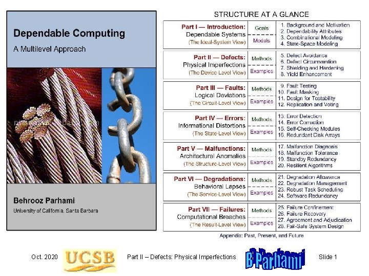
Oct. 2020 Part II – Defects: Physical Imperfections Slide 1

About This Presentation This presentation is intended to support the use of the textbook Dependable Computing: A Multilevel Approach (traditional print or on-line open publication, TBD). It is updated regularly by the author as part of his teaching of the graduate course ECE 257 A, Fault-Tolerant Computing, at Univ. of California, Santa Barbara. Instructors can use these slides freely in classroom teaching or for other educational purposes. Unauthorized uses, including distribution for profit, are strictly prohibited. © Behrooz Parhami Edition Released Revised First Sep. 2006 Oct. 2007 Oct. 2009 Oct. 2012 Oct. 2013 Jan. 2015 Oct. 2018 Oct. 2019 Oct. 2020 Part II – Defects: Physical Imperfections Slide 2

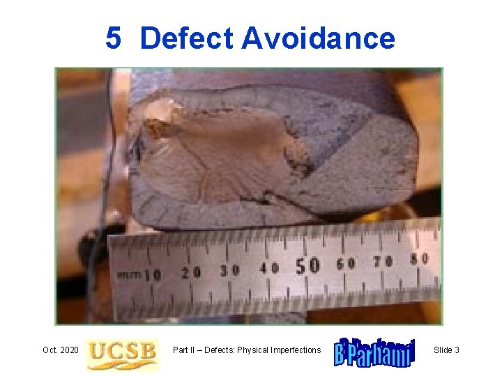
5 Defect Avoidance Oct. 2020 Part II – Defects: Physical Imperfections Slide 3

Oct. 2020 Part II – Defects: Physical Imperfections Slide 4

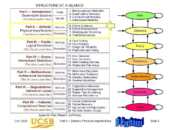
Oct. 2020 Part II – Defects: Physical Imperfections Slide 5

5. 1 Types and Causes of Defects Resistive open due to unfilled via [R. Madge et al. , IEEE D&T, 2003] Oct. 2020 Particle embedded between layers Part II – Defects: Physical Imperfections Slide 6

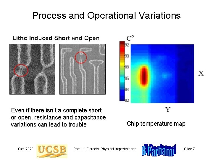
Process and Operational Variations Even if there isn’t a complete short or open, resistance and capacitance variations can lead to trouble Oct. 2020 Chip temperature map Part II – Defects: Physical Imperfections Slide 7

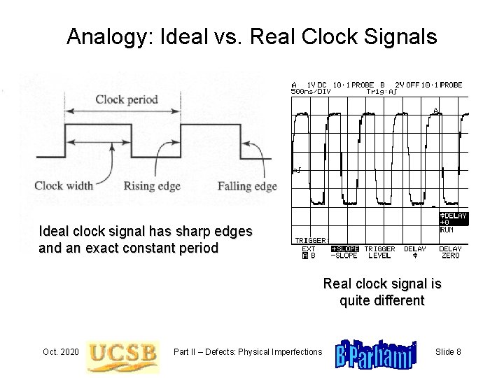
Analogy: Ideal vs. Real Clock Signals Ideal clock signal has sharp edges and an exact constant period Real clock signal is quite different Oct. 2020 Part II – Defects: Physical Imperfections Slide 8

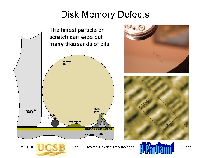
Disk Memory Defects The tiniest particle or scratch can wipe out many thousands of bits Oct. 2020 Part II – Defects: Physical Imperfections Slide 9

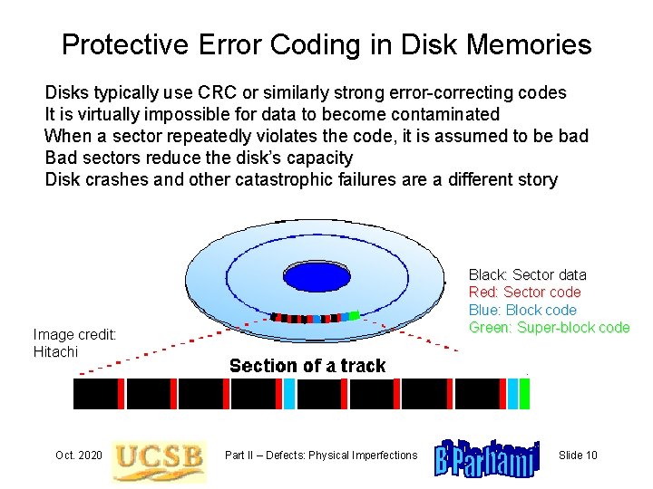
Protective Error Coding in Disk Memories Disks typically use CRC or similarly strong error-correcting codes It is virtually impossible for data to become contaminated When a sector repeatedly violates the code, it is assumed to be bad Bad sectors reduce the disk’s capacity Disk crashes and other catastrophic failures are a different story Black: Sector data Red: Sector code Blue: Block code Green: Super-block code Image credit: Hitachi Oct. 2020 Part II – Defects: Physical Imperfections Slide 10

Learning from Failed Disk Drives Analyses of failed disk drives have led to the following monitoring suggestions to predict when a disk drive is about to go, thus allowing a preemptive replacement before a hard failure Head flying height: Downward trend often precedes a head crash Number of remapped sectors: A bad sector is remapped to a different physical location on disk to avoid repeat errors, so having too many remapped sectors signal persistent problems Frequency of error correction via the built-in code: Disks routinely use CRC and other coding schemes to protect against data loss, but as errors accumulate, they may go beyond the code’s tolerance limit The following are signs of mechanical or electrical problems: - Changes in spin-up time - Rising temperatures in the unit - Reduction in data throughput Oct. 2020 Part II – Defects: Physical Imperfections Slide 11

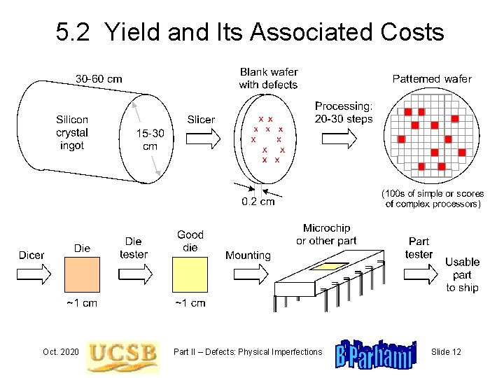
5. 2 Yield and Its Associated Costs Oct. 2020 Part II – Defects: Physical Imperfections Slide 12

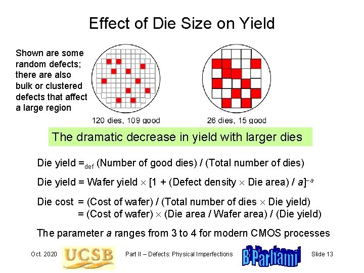
Effect of Die Size on Yield Shown are some random defects; there also bulk or clustered defects that affect a large region The dramatic decrease in yield with larger dies Die yield =def (Number of good dies) / (Total number of dies) Die yield = Wafer yield [1 + (Defect density Die area) / a]–a Die cost = (Cost of wafer) / (Total number of dies Die yield) = (Cost of wafer) (Die area / Wafer area) / (Die yield) The parameter a ranges from 3 to 4 for modern CMOS processes Oct. 2020 Part II – Defects: Physical Imperfections Slide 13

Effects of Yield on Testing and Part Reliability Assume a die yield of 50% Out of 2, 000 dies manufactured, 1, 000 are defective To achieve the goal of 100 defects per million (DPM) in parts shipped, we must catch 999, 900 of the 1, 000 defective parts Therefore, we need a test coverage of 99. 99% Testing is imperfect: missed defects/faults (coverage), false positives Going from a coverage of 99. 9% to 99. 99% involves a significant investment in test development and application times False positives are not a source of difficulty in this context Discarding another 1 -2% due to false positives in testing does not change the scale of the loss Oct. 2020 Part II – Defects: Physical Imperfections Slide 14

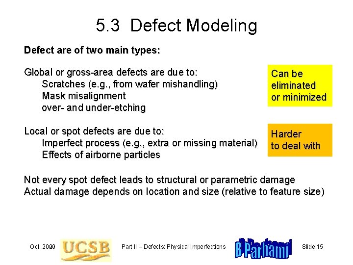
5. 3 Defect Modeling Defect are of two main types: Global or gross-area defects are due to: Scratches (e. g. , from wafer mishandling) Mask misalignment over- and under-etching Can be eliminated or minimized Local or spot defects are due to: Imperfect process (e. g. , extra or missing material) Effects of airborne particles Harder to deal with Not every spot defect leads to structural or parametric damage Actual damage depends on location and size (relative to feature size) Oct. 2009 2020 Part II – Defects: Physical Imperfections Slide 15

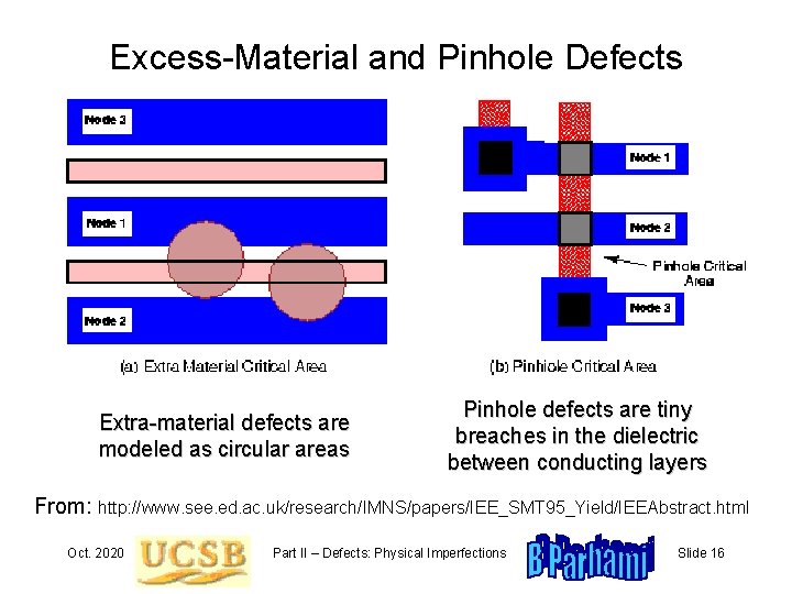
Excess-Material and Pinhole Defects Extra-material defects are modeled as circular areas Pinhole defects are tiny breaches in the dielectric between conducting layers From: http: //www. see. ed. ac. uk/research/IMNS/papers/IEE_SMT 95_Yield/IEEAbstract. html Oct. 2020 Part II – Defects: Physical Imperfections Slide 16

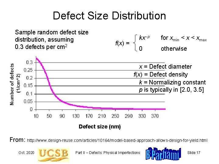
Defect Size Distribution Sample random defect size distribution, assuming 0. 3 defects per cm 2 f(x) = kx–p for xmin < xmax 0 otherwise x = Defect diameter f(x) = Defect density k = Normalizing constant p is typically in [2. 0, 3. 5] Defect size (nm) From: http: //www. design-reuse. com/articles/10164/model-based-approach-allows-design-for-yield. html Oct. 2020 Part II – Defects: Physical Imperfections Slide 17

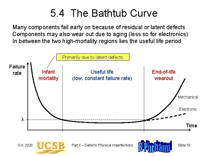
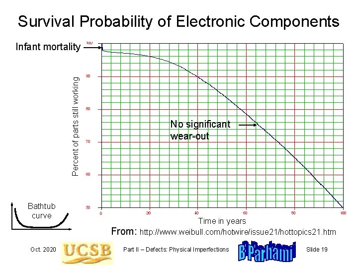
5. 4 The Bathtub Curve Many components fail early on because of residual or latent defects Components may also wear out due to aging (less so for electronics) In between the two high-mortality regions lies the useful life period Primarily due to latent defects Failure rate Infant mortality Useful life (low, constant failure rate) End-of-life wearout Mechanical Electronic l Time Oct. 2020 Part II – Defects: Physical Imperfections Slide 18

Survival Probability of Electronic Components Percent of parts still working Infant mortality No significant wear-out Bathtub curve From: Oct. 2020 Time in years http: //www. weibull. com/hotwire/issue 21/hottopics 21. htm Part II – Defects: Physical Imperfections Slide 19

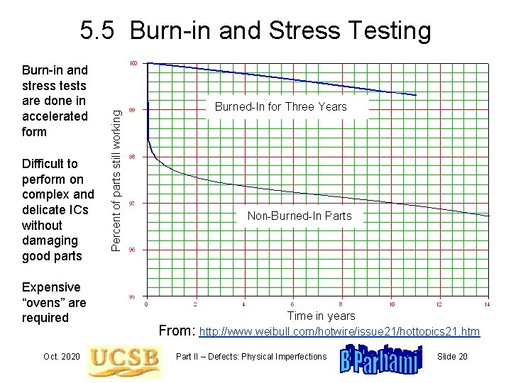
Burn-in and stress tests are done in accelerated form Difficult to perform on complex and delicate ICs without damaging good parts Expensive “ovens” are required Oct. 2020 Percent of parts still working 5. 5 Burn-in and Stress Testing From: Time in years http: //www. weibull. com/hotwire/issue 21/hottopics 21. htm Part II – Defects: Physical Imperfections Slide 20

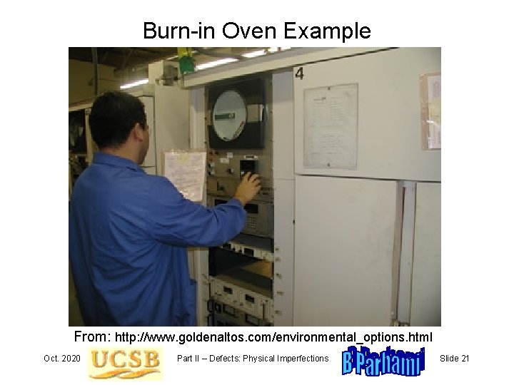
Burn-in Oven Example From: http: //www. goldenaltos. com/environmental_options. html Oct. 2020 Part II – Defects: Physical Imperfections Slide 21

5. 6 Active Defect Prevention Other than initial or manufacturing imperfections, defects can develop over the course of a device’s lifetime Defects induced by harsh operating environment Temperature control Load redistribution Clock scaling Radiation-induced defects Defects due to shock and vibration Defects due to mishandling (e. g. , scratch or smudge on disk). . . discussed in Chap. 7 dealing with shielding and hardening Oct. 2020 Part II – Defects: Physical Imperfections Slide 22

6 Defect Circumvention Oct. 2020 Part II – Defects: Physical Imperfections Slide 23

“This just in: the inhabitants of planet Earth are being recalled for the correction of a major defect. ” Oct. 2020 Part II – Defects: Physical Imperfections Slide 24

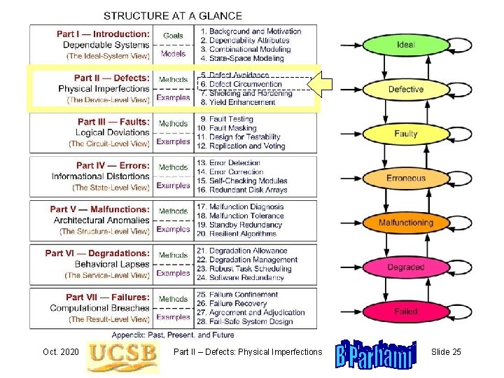
Oct. 2020 Part II – Defects: Physical Imperfections Slide 25

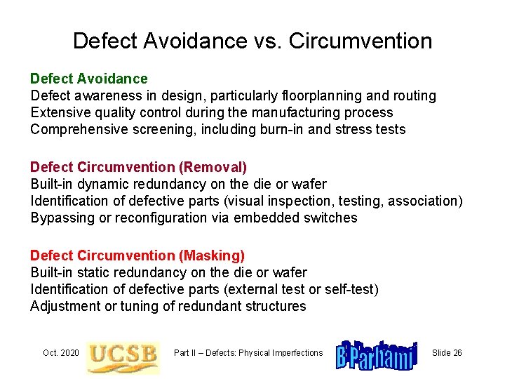
Defect Avoidance vs. Circumvention Defect Avoidance Defect awareness in design, particularly floorplanning and routing Extensive quality control during the manufacturing process Comprehensive screening, including burn-in and stress tests Defect Circumvention (Removal) Built-in dynamic redundancy on the die or wafer Identification of defective parts (visual inspection, testing, association) Bypassing or reconfiguration via embedded switches Defect Circumvention (Masking) Built-in static redundancy on the die or wafer Identification of defective parts (external test or self-test) Adjustment or tuning of redundant structures Oct. 2020 Part II – Defects: Physical Imperfections Slide 26

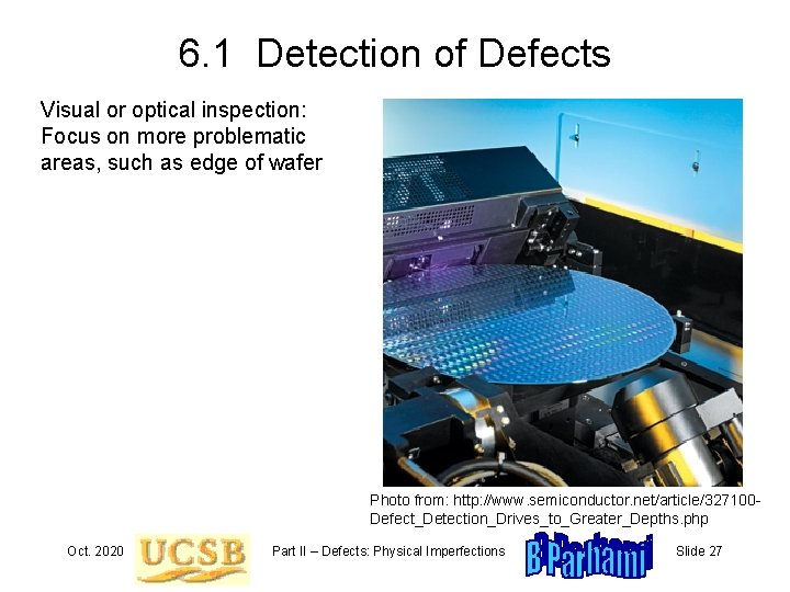
6. 1 Detection of Defects Visual or optical inspection: Focus on more problematic areas, such as edge of wafer Photo from: http: //www. semiconductor. net/article/327100 Defect_Detection_Drives_to_Greater_Depths. php Oct. 2020 Part II – Defects: Physical Imperfections Slide 27

6. 2 Redundancy and Reconfiguration Works best when the system on die has regular, repetitive structure: Memory FPGA Multicore chip CMP (chip multiprocessor) Irregular (random) logic implies greater redundancy due to replication: Replicated structures must not be close to each other They should not be very far either (wiring/switching overhead) Oct. 2020 Part II – Defects: Physical Imperfections Slide 28

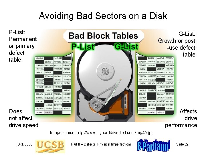
Avoiding Bad Sectors on a Disk P-List: Permanent or primary defect table G-List: Growth or post -use defect table Does not affect drive speed Affects drive performance Image source: http: //www. myharddrivedied. com/img 4 A. jpg Oct. 2020 Part II – Defects: Physical Imperfections Slide 29

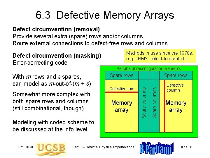
6. 3 Defective Memory Arrays Defect circumvention (removal) Provide several extra (spare) rows and/or columns Route external connections to defect-free rows and columns Defect circumvention (masking) Error-correcting code Methods in use since the 1970 s; e. g. , IBM’s defect-tolerant chip Peripheral reconfiguration elements Spare rows Defective row Defective column Memory array Spare columns Somewhat more complex with both spare rows and columns (still combinational, though) Spare rows Spare columns With m rows and s spares, can model as m-out-of-(m + s) Memory array Modeling with coded scheme to be discussed at the info level Oct. 2020 Part II – Defects: Physical Imperfections Slide 30

6. 4 Defects in Logic and FPGAs Moore and Shannon’s pioneering work: Building arbitrarily reliable relay circuits out of “crummy” relays Prob. that a relay device closes when it is supposed to be open = p Prob. that a relay circuit closes when it is supposed to be open = h(p) If we can achieve h(p) < p, then repeated application of the composition scheme will lead to arbitrarily small h(h(h(. . . h(p)))) x x h(p) = 4 p 2 – 4 p 3 + p 4 h(p) < p for p < 0. 382 x x h(p) > p for p > 0. 382 p Oct. 2020 Part II – Defects: Physical Imperfections Slide 31

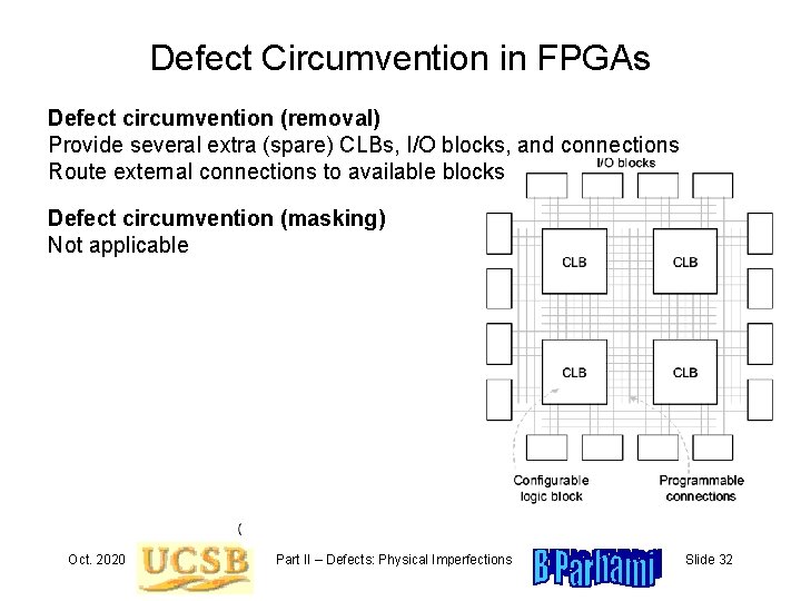
Defect Circumvention in FPGAs Defect circumvention (removal) Provide several extra (spare) CLBs, I/O blocks, and connections Route external connections to available blocks Defect circumvention (masking) Not applicable Oct. 2020 Part II – Defects: Physical Imperfections Slide 32

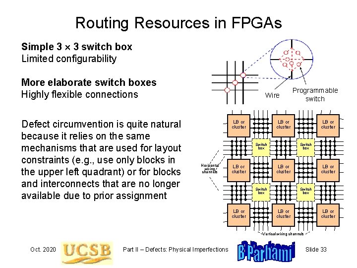
Routing Resources in FPGAs Simple 3 3 switch box Limited configurability More elaborate switch boxes Highly flexible connections Defect circumvention is quite natural because it relies on the same mechanisms that are used for layout constraints (e. g. , use only blocks in the upper left quadrant) or for blocks and interconnects that are no longer available due to prior assignment Wire LB or cluster Switch box LB or cluster Switch box Horizontal wiring channels Programmable switch LB or cluster Switch box LB or cluster Vertical wiring channels Oct. 2020 Part II – Defects: Physical Imperfections Slide 33

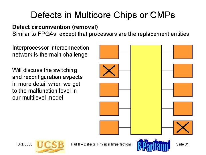
Defects in Multicore Chips or CMPs Defect circumvention (removal) Similar to FPGAs, except that processors are the replacement entities Interprocessor interconnection network is the main challenge Will discuss the switching and reconfiguration aspects in more detail when we get to the malfunction level in our multilevel model Oct. 2020 Part II – Defects: Physical Imperfections Slide 34

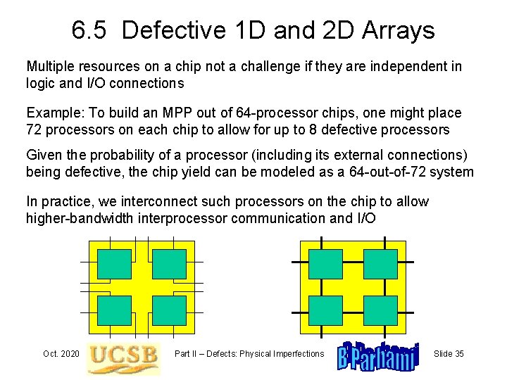
6. 5 Defective 1 D and 2 D Arrays Multiple resources on a chip not a challenge if they are independent in logic and I/O connections Example: To build an MPP out of 64 -processor chips, one might place 72 processors on each chip to allow for up to 8 defective processors Given the probability of a processor (including its external connections) being defective, the chip yield can be modeled as a 64 -out-of-72 system In practice, we interconnect such processors on the chip to allow higher-bandwidth interprocessor communication and I/O Oct. 2020 Part II – Defects: Physical Imperfections Slide 35

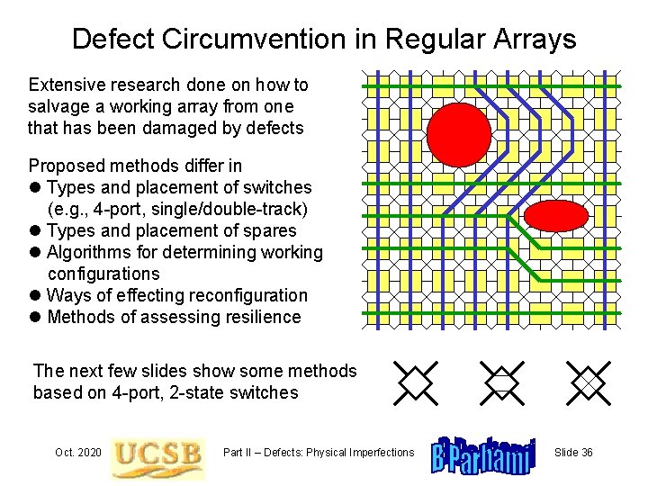
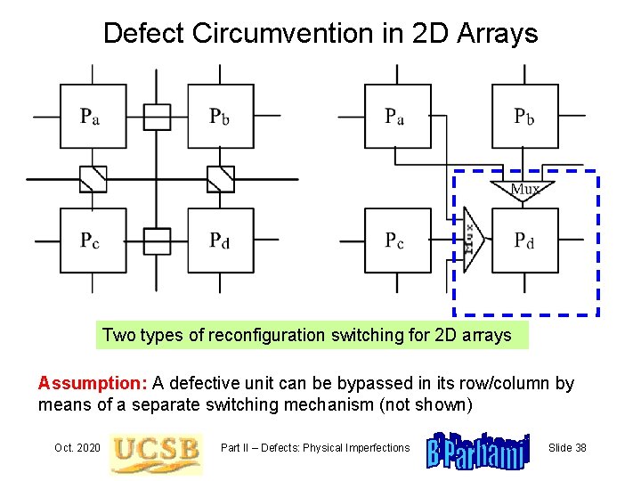
Defect Circumvention in Regular Arrays Extensive research done on how to salvage a working array from one that has been damaged by defects Proposed methods differ in Types and placement of switches (e. g. , 4 -port, single/double-track) Types and placement of spares Algorithms for determining working configurations Ways of effecting reconfiguration Methods of assessing resilience The next few slides show some methods based on 4 -port, 2 -state switches Oct. 2020 Part II – Defects: Physical Imperfections Slide 36

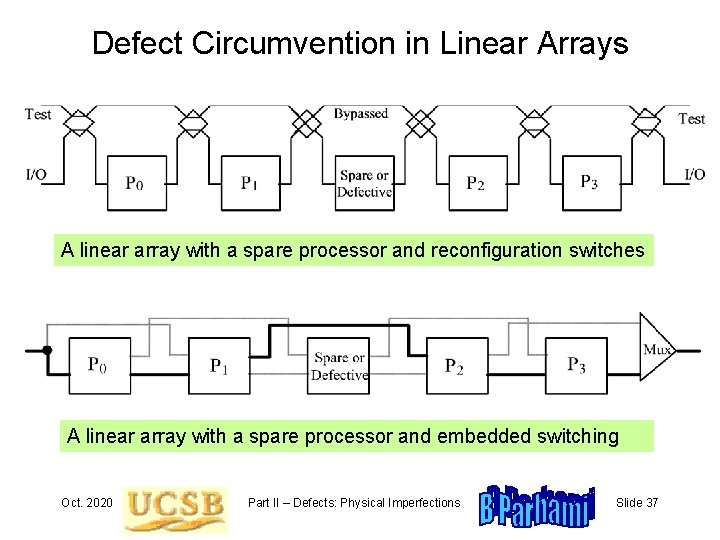
Defect Circumvention in Linear Arrays A linear array with a spare processor and reconfiguration switches A linear array with a spare processor and embedded switching Oct. 2020 Part II – Defects: Physical Imperfections Slide 37

Defect Circumvention in 2 D Arrays Two types of reconfiguration switching for 2 D arrays Assumption: A defective unit can be bypassed in its row/column by means of a separate switching mechanism (not shown) Oct. 2020 Part II – Defects: Physical Imperfections Slide 38

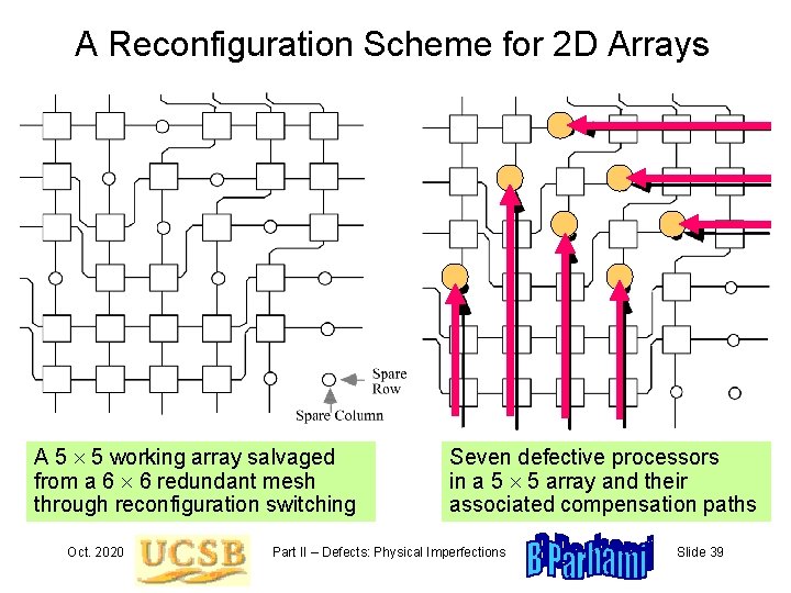
A Reconfiguration Scheme for 2 D Arrays A 5 5 working array salvaged from a 6 6 redundant mesh through reconfiguration switching Oct. 2020 Seven defective processors in a 5 5 array and their associated compensation paths Part II – Defects: Physical Imperfections Slide 39

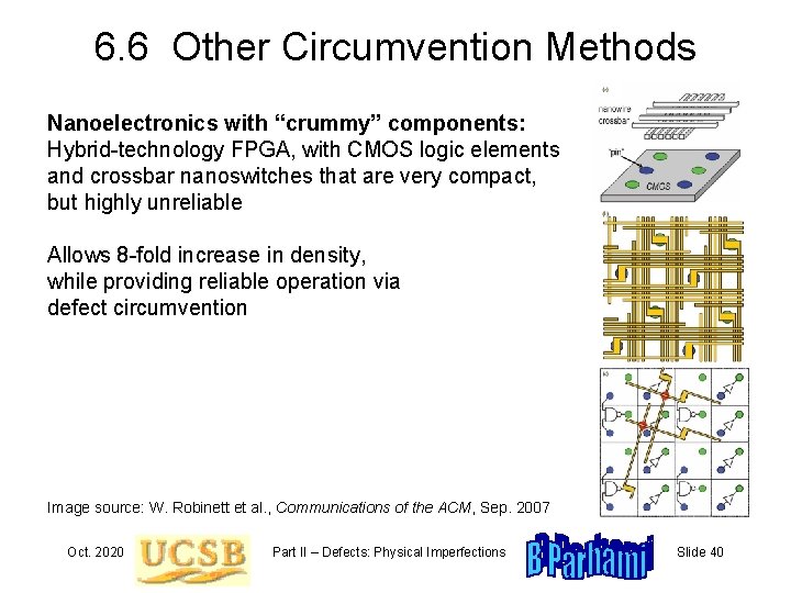
6. 6 Other Circumvention Methods Nanoelectronics with “crummy” components: Hybrid-technology FPGA, with CMOS logic elements and crossbar nanoswitches that are very compact, but highly unreliable Allows 8 -fold increase in density, while providing reliable operation via defect circumvention Image source: W. Robinett et al. , Communications of the ACM, Sep. 2007 Oct. 2020 Part II – Defects: Physical Imperfections Slide 40

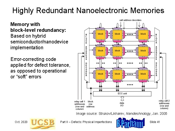
Highly Redundant Nanoelectronic Memories Memory with block-level redundancy: Based on hybrid semiconductor/nanodevice implementation Error-correcting code applied for defect tolerance, as opposed to operational or “soft” errors Image source: Strukov/Likharev, Nanotechnology, Jan. 2005 Oct. 2020 Part II – Defects: Physical Imperfections Slide 41

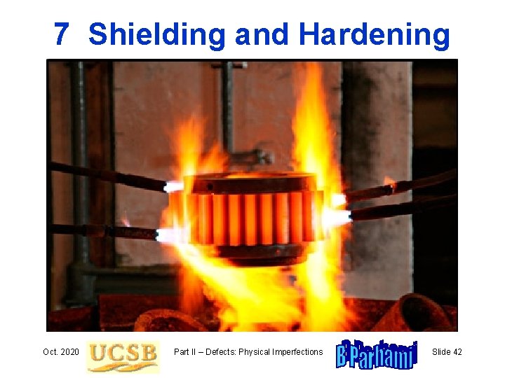
7 Shielding and Hardening Oct. 2020 Part II – Defects: Physical Imperfections Slide 42

Oct. 2020 Part II – Defects: Physical Imperfections Slide 43

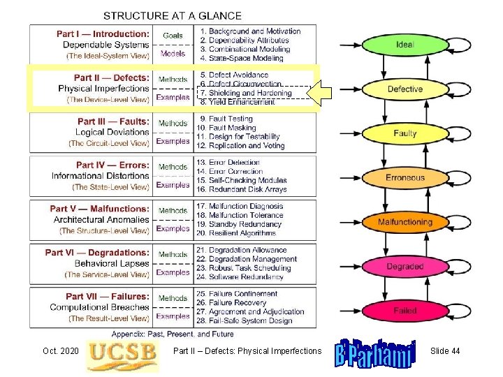
Oct. 2020 Part II – Defects: Physical Imperfections Slide 44

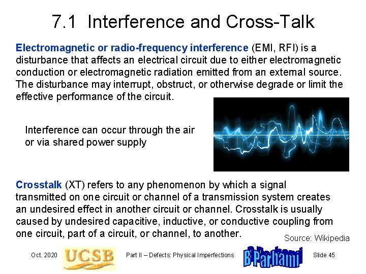
7. 1 Interference and Cross-Talk Electromagnetic or radio-frequency interference (EMI, RFI) is a disturbance that affects an electrical circuit due to either electromagnetic conduction or electromagnetic radiation emitted from an external source. The disturbance may interrupt, obstruct, or otherwise degrade or limit the effective performance of the circuit. Interference can occur through the air or via shared power supply Crosstalk (XT) refers to any phenomenon by which a signal transmitted on one circuit or channel of a transmission system creates an undesired effect in another circuit or channel. Crosstalk is usually caused by undesired capacitive, inductive, or conductive coupling from one circuit, part of a circuit, or channel, to another. Source: Wikipedia Oct. 2020 Part II – Defects: Physical Imperfections Slide 45

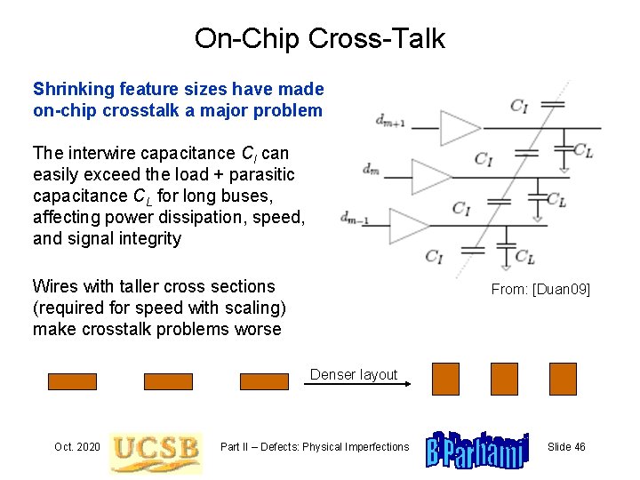
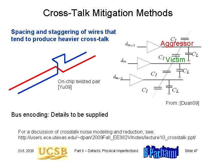
On-Chip Cross-Talk Shrinking feature sizes have made on-chip crosstalk a major problem The interwire capacitance CI can easily exceed the load + parasitic capacitance CL for long buses, affecting power dissipation, speed, and signal integrity Wires with taller cross sections (required for speed with scaling) make crosstalk problems worse From: [Duan 09] Denser layout Oct. 2020 Part II – Defects: Physical Imperfections Slide 46

Cross-Talk Mitigation Methods Spacing and staggering of wires that tend to produce heavier cross-talk Aggressor Victim On-chip twisted pair [Yu 09] From: [Duan 09] Bus encoding: Details to be supplied For a discussion of crosstalk noise modeling and reduction, see: http: //users. ece. utexas. edu/~dpan/2009 Fall_EE 382 V/notes/lecture 10_crosstalk. ppt/ Oct. 2020 Part II – Defects: Physical Imperfections Slide 47

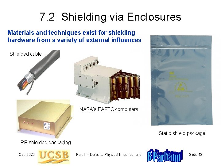
7. 2 Shielding via Enclosures Materials and techniques exist for shielding hardware from a variety of external influences Shielded cable NASA’s EAFTC computers Static-shield package RF-shielded packaging Oct. 2020 Part II – Defects: Physical Imperfections Slide 48

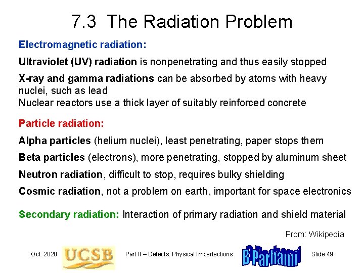
7. 3 The Radiation Problem Electromagnetic radiation: Ultraviolet (UV) radiation is nonpenetrating and thus easily stopped X-ray and gamma radiations can be absorbed by atoms with heavy nuclei, such as lead Nuclear reactors use a thick layer of suitably reinforced concrete Particle radiation: Alpha particles (helium nuclei), least penetrating, paper stops them Beta particles (electrons), more penetrating, stopped by aluminum sheet Neutron radiation, difficult to stop, requires bulky shielding Cosmic radiation, not a problem on earth, important for space electronics Secondary radiation: Interaction of primary radiation and shield material From: Wikipedia Oct. 2020 Part II – Defects: Physical Imperfections Slide 49

Radiation Effect on CMOS ICs Impact by high-energy particles, such as protons or heavy ions Radiation ionizes the oxide, creating electrons and holes; the electrons then flow out, creating a positive charge which leads to current leak across the channel It also decreases the threshold voltage, which affects timing and other operational parameters From: http: //ajnoyola. com/RHBD_primer. html One-way mission to Mars: Exposes the electronics to about 1000 kilorad of radiation, which is near the limit of what is now tolerable by advanced space electronics Oct. 2020 Part II – Defects: Physical Imperfections Slide 50

Heavy-Ion and Proton Radiations From: http: //parts. jpl. nasa. gov/docs/Radcrs_Final. pdf Oct. 2020 Part II – Defects: Physical Imperfections Slide 51

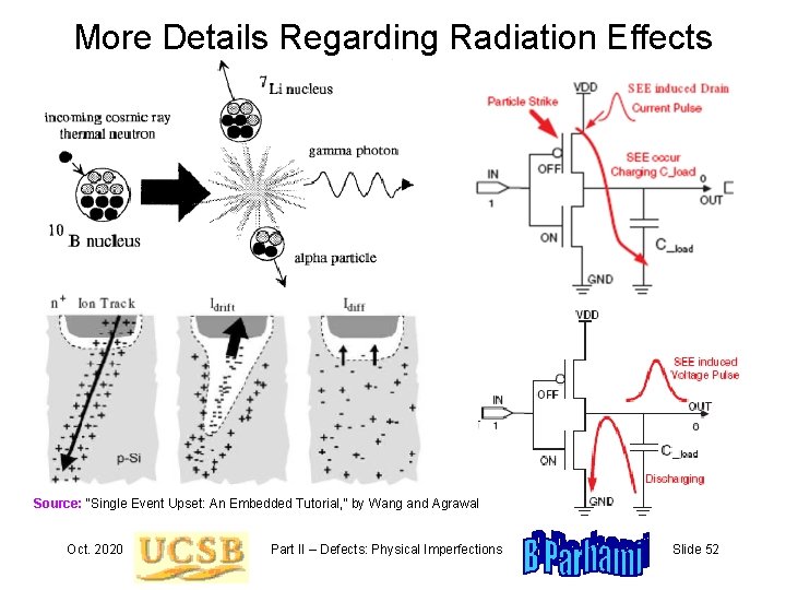
More Details Regarding Radiation Effects Source: “Single Event Upset: An Embedded Tutorial, ” by Wang and Agrawal Oct. 2020 Part II – Defects: Physical Imperfections Slide 52

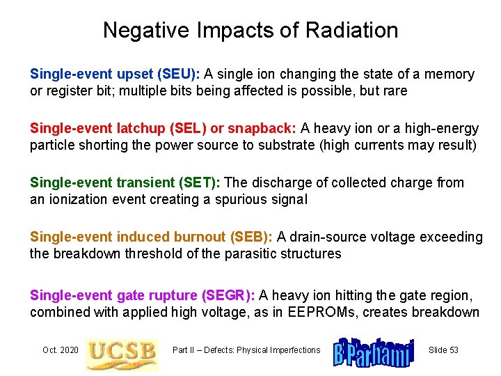
Negative Impacts of Radiation Single-event upset (SEU): A single ion changing the state of a memory or register bit; multiple bits being affected is possible, but rare Single-event latchup (SEL) or snapback: A heavy ion or a high-energy particle shorting the power source to substrate (high currents may result) Single-event transient (SET): The discharge of collected charge from an ionization event creating a spurious signal Single-event induced burnout (SEB): A drain-source voltage exceeding the breakdown threshold of the parasitic structures Single-event gate rupture (SEGR): A heavy ion hitting the gate region, combined with applied high voltage, as in EEPROMs, creates breakdown Oct. 2020 Part II – Defects: Physical Imperfections Slide 53

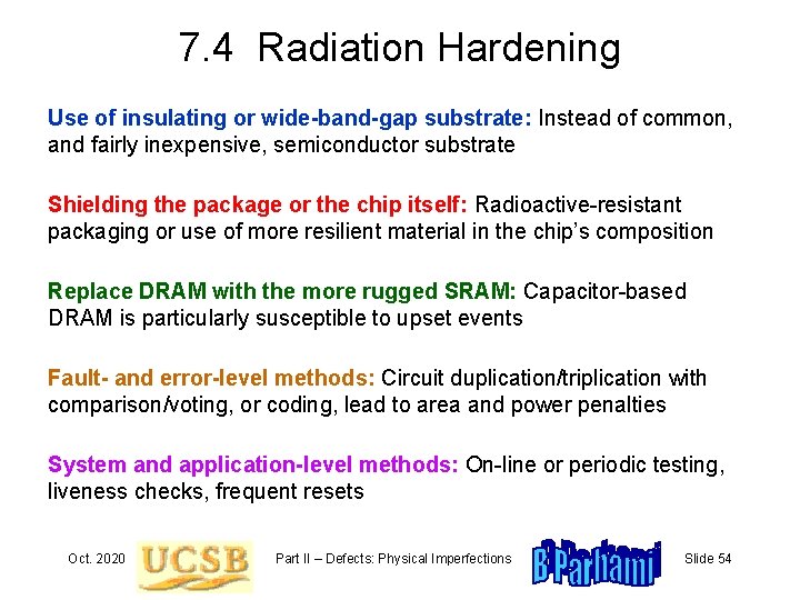
7. 4 Radiation Hardening Use of insulating or wide-band-gap substrate: Instead of common, and fairly inexpensive, semiconductor substrate Shielding the package or the chip itself: Radioactive-resistant packaging or use of more resilient material in the chip’s composition Replace DRAM with the more rugged SRAM: Capacitor-based DRAM is particularly susceptible to upset events Fault- and error-level methods: Circuit duplication/triplication with comparison/voting, or coding, lead to area and power penalties System and application-level methods: On-line or periodic testing, liveness checks, frequent resets Oct. 2020 Part II – Defects: Physical Imperfections Slide 54

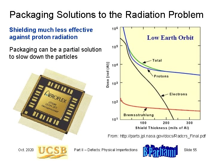
Packaging Solutions to the Radiation Problem Shielding much less effective against proton radiation Packaging can be a partial solution to slow down the particles From: http: //parts. jpl. nasa. gov/docs/Radcrs_Final. pdf Oct. 2020 Part II – Defects: Physical Imperfections Slide 55

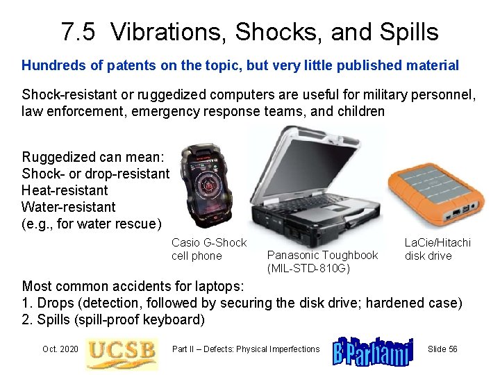
7. 5 Vibrations, Shocks, and Spills Hundreds of patents on the topic, but very little published material Shock-resistant or ruggedized computers are useful for military personnel, law enforcement, emergency response teams, and children Ruggedized can mean: Shock- or drop-resistant Heat-resistant Water-resistant (e. g. , for water rescue) Casio G-Shock cell phone Panasonic Toughbook (MIL-STD-810 G) La. Cie/Hitachi disk drive Most common accidents for laptops: 1. Drops (detection, followed by securing the disk drive; hardened case) 2. Spills (spill-proof keyboard) Oct. 2020 Part II – Defects: Physical Imperfections Slide 56

Rugged Laptop for NASA’s Space Shuttles The GRi. D (Graphical Retrieval Information Display) Compass First laptop in orbit First with a clamshell design 21. 6 -cm bright plasma display In use through the early 1990 s Weight: 4. 5 kg Cost: $8150, at the time Reportedly survived the 1986 Space Shuttle Challenger crash Image credit: IEEE Spectrum Oct. 2020 Part II – Defects: Physical Imperfections Slide 57

7. 6 Current Practice and Trends This section to be completed Nemoto, N. , et al. “Evaluation of Single-Event Upset Tolerance on Recent Commercial Memory ICs” Proc. 3 rd ESA Electronic Components Conf. , April 1997 Abstract: Single-event upset (SEU) tolerance for commercial 1 Mbit SRAMs, 4 Mbit SRAMs, 16 Mbit DRAMs and 64 Mbit DRAMs was evaluated by irradiation tests using high-energy heavy ions with an LET range between 4. 0 and 60. 6 Me. V/(mg/cm 2). The threshold LET and the saturated cross-section were determined for each device from the LET dependence of the SEU cross-section. We show these test results and describe the SEU tolerance of highly integrated memory devices in connection with their structures and fabrication processes. The SEU rates in actual space were also calculated for these devices. Oct. 2020 Part II – Defects: Physical Imperfections Slide 58

8 Yield Enhancement Oct. 2020 Part II – Defects: Physical Imperfections Slide 59

Oct. 2020 Part II – Defects: Physical Imperfections Slide 60

Oct. 2020 Part II – Defects: Physical Imperfections Slide 61

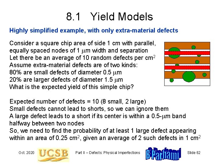
8. 1 Yield Models Highly simplified example, with only extra-material defects Consider a square chip area of side 1 cm with parallel, equally spaced nodes of 1 mm width and separation Let there be an average of 10 random defects per cm 2 Assume extra-material defects are of two kinds: 80% are small defects of diameter 0. 5 mm 20% are larger defects of diameter 1. 5 mm What is the expected yield of this simple chip? Expected number of defects = 10 (8 small, 2 large) Small defects cannot lead to shorts, so we can ignore them A large defect leads to a short if its center is within a 0. 5 -mm band halfway between two nodes So, we need to find the probability of at least 1 large defect appearing within an area of 0. 25 cm 2, given an average of 2 such defects in 1 cm 2 Oct. 2020 Part II – Defects: Physical Imperfections Slide 62

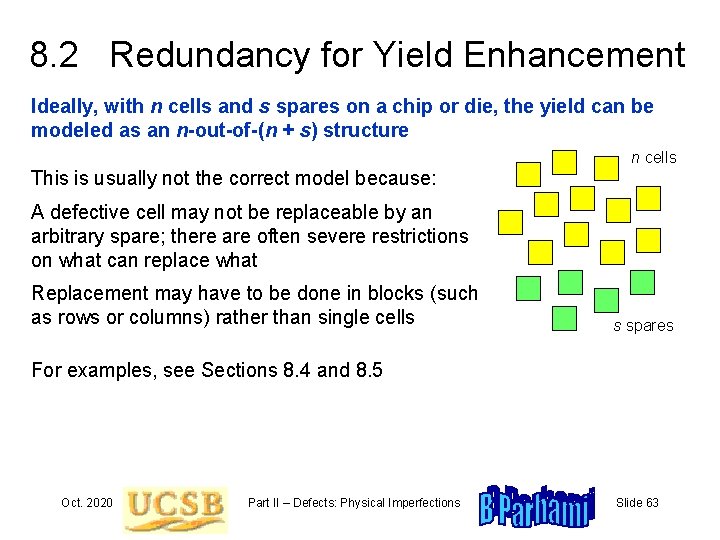
8. 2 Redundancy for Yield Enhancement Ideally, with n cells and s spares on a chip or die, the yield can be modeled as an n-out-of-(n + s) structure n cells This is usually not the correct model because: A defective cell may not be replaceable by an arbitrary spare; there are often severe restrictions on what can replace what Replacement may have to be done in blocks (such as rows or columns) rather than single cells s spares For examples, see Sections 8. 4 and 8. 5 Oct. 2020 Part II – Defects: Physical Imperfections Slide 63

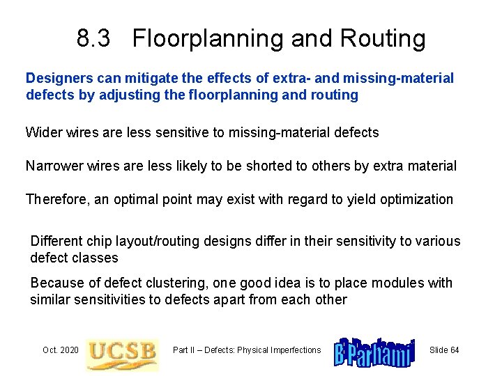
8. 3 Floorplanning and Routing Designers can mitigate the effects of extra- and missing-material defects by adjusting the floorplanning and routing Wider wires are less sensitive to missing-material defects Narrower wires are less likely to be shorted to others by extra material Therefore, an optimal point may exist with regard to yield optimization Different chip layout/routing designs differ in their sensitivity to various defect classes Because of defect clustering, one good idea is to place modules with similar sensitivities to defects apart from each other Oct. 2020 Part II – Defects: Physical Imperfections Slide 64

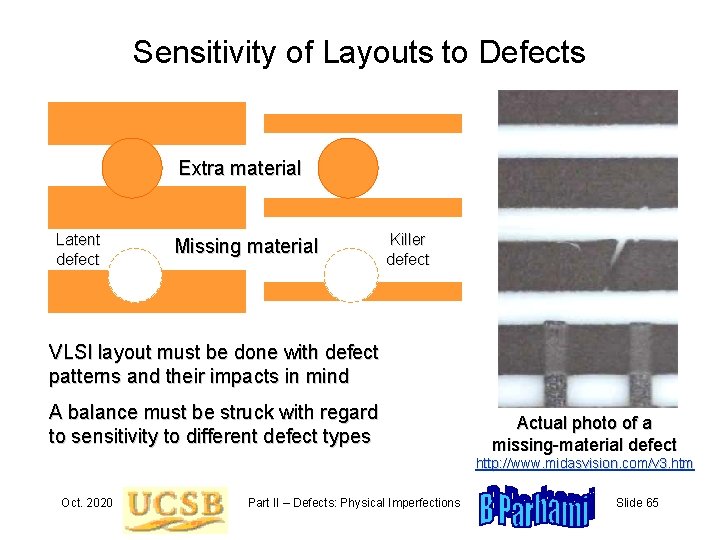
Sensitivity of Layouts to Defects Extra material Latent defect Missing material Killer defect VLSI layout must be done with defect patterns and their impacts in mind A balance must be struck with regard to sensitivity to different defect types Actual photo of a missing-material defect http: //www. midasvision. com/v 3. htm Oct. 2020 Part II – Defects: Physical Imperfections Slide 65

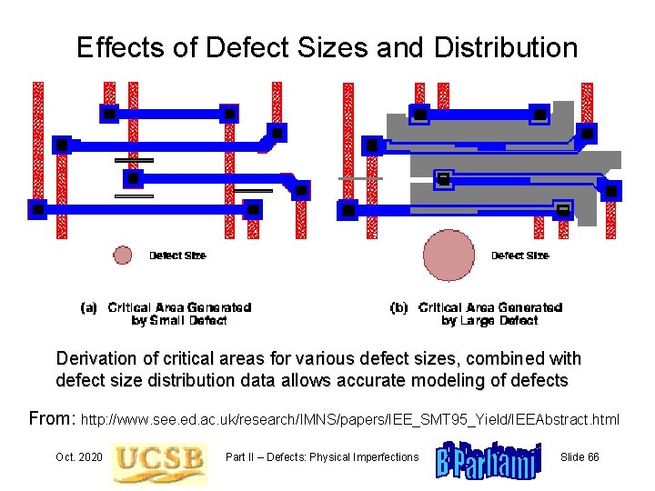
Effects of Defect Sizes and Distribution Derivation of critical areas for various defect sizes, combined with defect size distribution data allows accurate modeling of defects From: http: //www. see. ed. ac. uk/research/IMNS/papers/IEE_SMT 95_Yield/IEEAbstract. html Oct. 2020 Part II – Defects: Physical Imperfections Slide 66

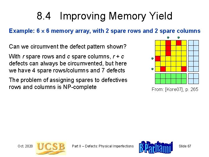
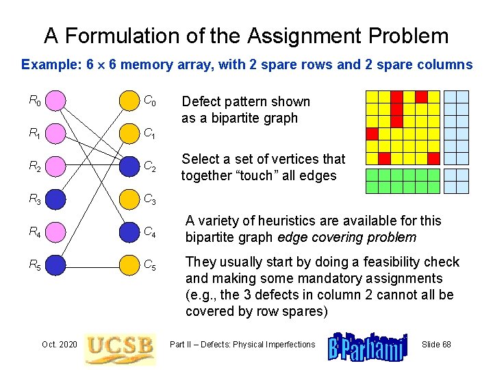
8. 4 Improving Memory Yield Example: 6 6 memory array, with 2 spare rows and 2 spare columns Can we circumvent the defect pattern shown? With r spare rows and c spare columns, r + c defects can always be circumvented, but here we have 4 spare rows/columns and 7 defects The problem of assigning spares to defectives rows and columns is NP-complete Oct. 2020 Part II – Defects: Physical Imperfections From: [Kore 07], p. 265 Slide 67

A Formulation of the Assignment Problem Example: 6 6 memory array, with 2 spare rows and 2 spare columns R 0 C 0 R 1 C 1 R 2 C 2 R 3 C 3 R 4 C 4 R 5 C 5 Oct. 2020 Defect pattern shown as a bipartite graph Select a set of vertices that together “touch” all edges A variety of heuristics are available for this bipartite graph edge covering problem They usually start by doing a feasibility check and making some mandatory assignments (e. g. , the 3 defects in column 2 cannot all be covered by row spares) Part II – Defects: Physical Imperfections Slide 68

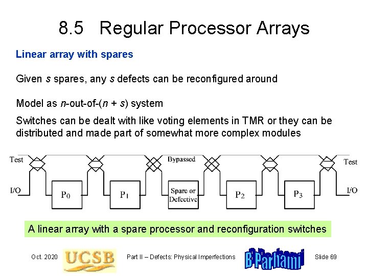
8. 5 Regular Processor Arrays Linear array with spares Given s spares, any s defects can be reconfigured around Model as n-out-of-(n + s) system Switches can be dealt with like voting elements in TMR or they can be distributed and made part of somewhat more complex modules A linear array with a spare processor and reconfiguration switches Oct. 2020 Part II – Defects: Physical Imperfections Slide 69

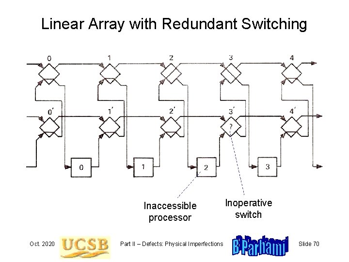
Linear Array with Redundant Switching Inaccessible processor Oct. 2020 Part II – Defects: Physical Imperfections Inoperative switch Slide 70

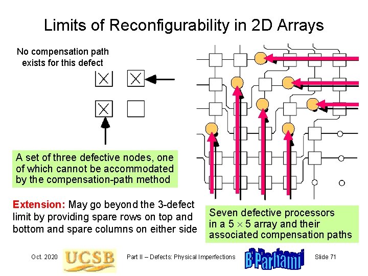
Limits of Reconfigurability in 2 D Arrays No compensation path exists for this defect A set of three defective nodes, one of which cannot be accommodated by the compensation-path method Extension: May go beyond the 3 -defect limit by providing spare rows on top and bottom and spare columns on either side Oct. 2020 Seven defective processors in a 5 5 array and their associated compensation paths Part II – Defects: Physical Imperfections Slide 71

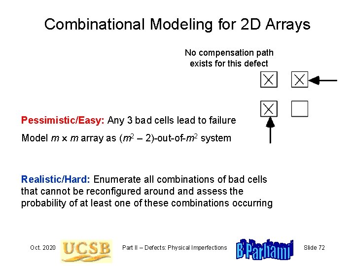
Combinational Modeling for 2 D Arrays No compensation path exists for this defect Pessimistic/Easy: Any 3 bad cells lead to failure Model m m array as (m 2 – 2)-out-of-m 2 system Realistic/Hard: Enumerate all combinations of bad cells that cannot be reconfigured around assess the probability of at least one of these combinations occurring Oct. 2020 Part II – Defects: Physical Imperfections Slide 72

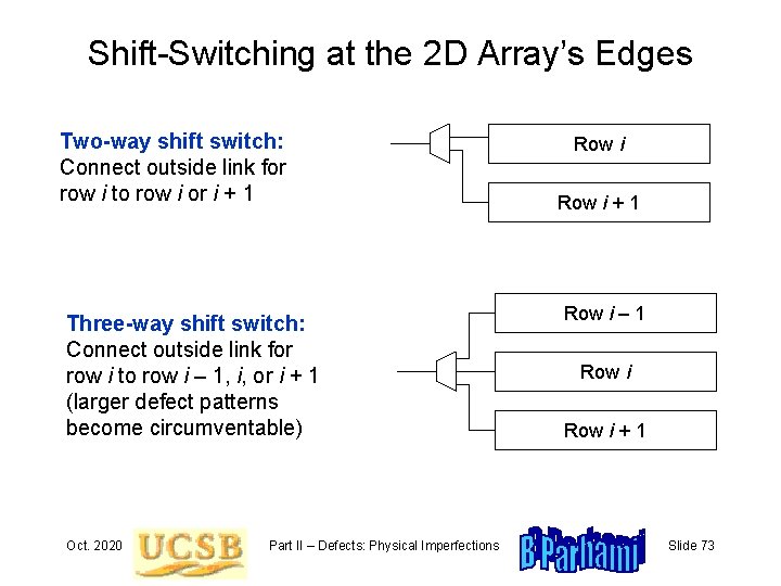
Shift-Switching at the 2 D Array’s Edges Two-way shift switch: Connect outside link for row i to row i or i + 1 Three-way shift switch: Connect outside link for row i to row i – 1, i, or i + 1 (larger defect patterns become circumventable) Oct. 2020 Part II – Defects: Physical Imperfections Row i + 1 Row i – 1 Row i + 1 Slide 73

Multiple Redundancy Schemes Multiple forms of redundancy can be effective for defect circumvention, if each method covers the others’ weaknesses Example: Memory yield enhancement ECC quite good in confronting isolated random defects Spare rows/columns/blocks good for correlated or large-area defects Oct. 2020 Part II – Defects: Physical Imperfections Slide 74

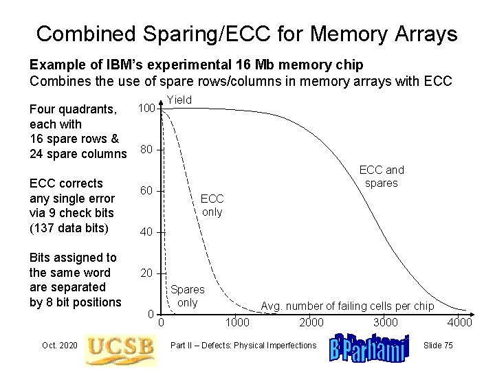
Combined Sparing/ECC for Memory Arrays Example of IBM’s experimental 16 Mb memory chip Combines the use of spare rows/columns in memory arrays with ECC Four quadrants, each with 16 spare rows & 24 spare columns ECC corrects any single error via 9 check bits (137 data bits) Bits assigned to the same word are separated by 8 bit positions Oct. 2020 Yield 100 80 ECC and spares 60 ECC only 40 20 0 Spares only 0 1000 Avg. number of failing cells per chip 2000 3000 Part II – Defects: Physical Imperfections 4000 Slide 75

8. 6 Impact of Process Variations Small feature sizes and high densities of modern VLSI circuits make slight manufacturing variations quite significant in their correct functioning and performance Additionally, there may be massive numbers of defects in nanoelectronic circuits and a single physical defect may affect more components than before Oct. 2020 Part II – Defects: Physical Imperfections Slide 76

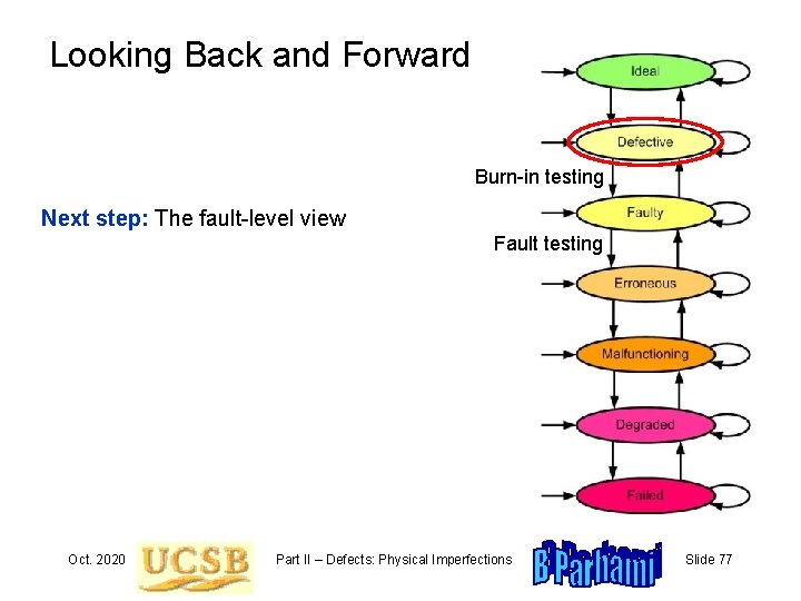
Looking Back and Forward Burn-in testing Next step: The fault-level view Fault testing Oct. 2020 Part II – Defects: Physical Imperfections Slide 77