
Obtencin caracterizacin y aplicaciones de dispositivos pticos basados
Obtención, caracterización y aplicaciones de dispositivos ópticos basados en nanoestructuras de silicio. Realisation, characterisation and applications of optical devices based on silicon nanostructures. Ph. D Thesis Defense Daniel Navarro Urrios Dpto. de Física Básica, Universidad de La Laguna Ph. D thesis defense, La Laguna, 5 -12 -2006 Daniel Navarro Urrios
Outline • General Introduction • Amplification studies in planar waveguides based on oxidised porous silicon • Form birefringence in Si-Nc planar waveguides • Er coupled to Si-Nc optical amplifiers • General conclusions Ph. D thesis defense, La Laguna, 5 -12 -2006 Daniel Navarro Urrios 2
Outline • General Introduction • Amplification studies in planar waveguides based on oxidised porous silicon • Form birefringence in Si-Nc planar waveguides • Er coupled to Si-Nc optical amplifiers • General conclusions Ph. D thesis defense, La Laguna, 5 -12 -2006 Daniel Navarro Urrios 3
General introduction • Silicon is the leading material for microelectronics. Huge processing technology (CMOS) infrastructure, process learning and capacity. • In photonics it can do also well (waveguides, fast modulators, power splitters and combiners, tuneable optical filters, detectors…) • It is the ideal plattform for integrating optical and electrical devices. Ph. D thesis defense, La Laguna, 5 -12 -2006 Daniel Navarro Urrios 4
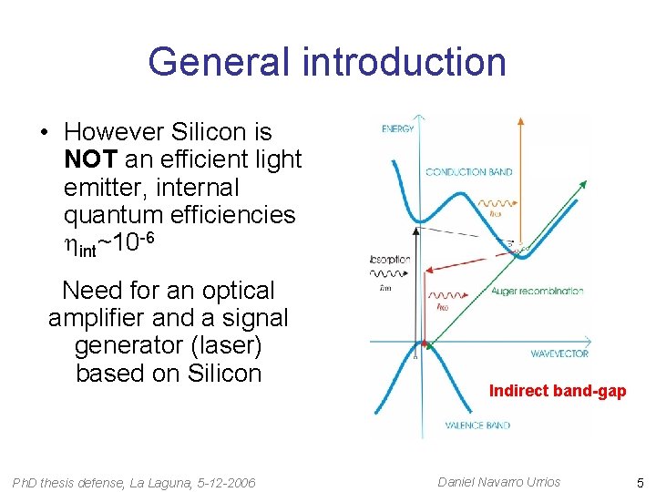
General introduction • However Silicon is NOT an efficient light emitter, internal quantum efficiencies int~10 -6 Need for an optical amplifier and a signal generator (laser) based on Silicon Ph. D thesis defense, La Laguna, 5 -12 -2006 Indirect band-gap Daniel Navarro Urrios 5
Different strategies to amplify light based on Silicon materials • Dye-doped planar waveguides based on oxidised porous silicon • Si-Nc in Si. O 2 planar waveguides • Er coupled to Si-Nc planar amplifiers Ph. D thesis defense, La Laguna, 5 -12 -2006 Daniel Navarro Urrios 6
Outline • General Introduction • Amplification studies in planar waveguides based on oxidised porous silicon • Form birefringence in Si-Nc planar waveguides • Er coupled to Si-Nc optical amplifiers • General conclusions Ph. D thesis defense, La Laguna, 5 -12 -2006 Daniel Navarro Urrios 7
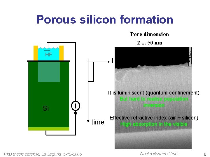
Porous silicon formation Pore dimension 2. . . 50 nm HF Si I It is luminiscent (quantum confinement) But hard to realise population inversion I time Ph. D thesis defense, La Laguna, 5 -12 -2006 Effective refractive index (air + silicon) High absorption in the visible Daniel Navarro Urrios 8
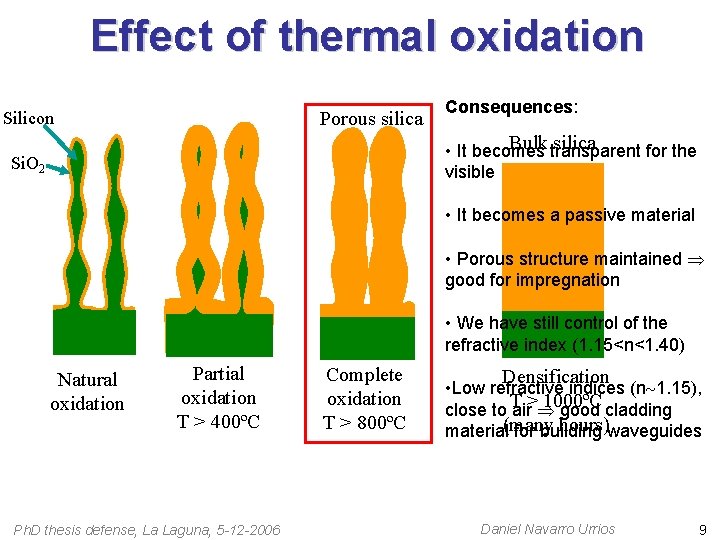
Effect of thermal oxidation Porous silica Silicon Consequences: Bulk silica • It becomes transparent for the visible Si. O 2 • It becomes a passive material • Porous structure maintained good for impregnation • We have still control of the refractive index (1. 15<n<1. 40) Natural oxidation Partial oxidation T > 400ºC Ph. D thesis defense, La Laguna, 5 -12 -2006 Complete oxidation T > 800ºC Densification • Low refractive indices (n 1. 15), T > 1000ºC close to air good cladding (many hours) material for building waveguides Daniel Navarro Urrios 9
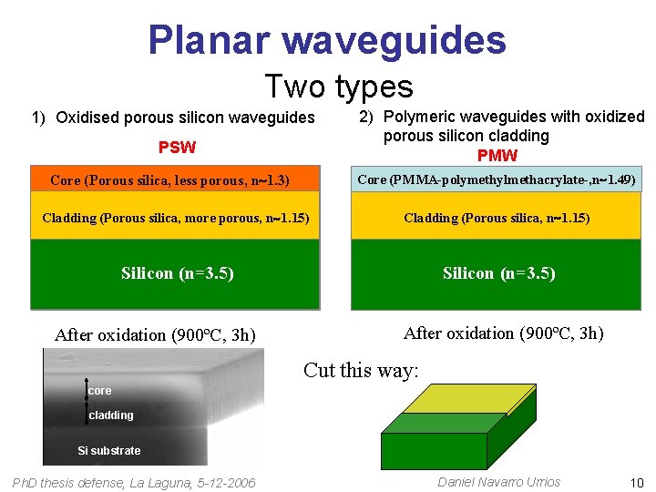
Planar waveguides Two types 1) Oxidised porous silicon waveguides PSW 2) Polymeric waveguides with oxidized porous silicon cladding PMW Core less porous, n 1. 3) Core(Poroussilica, silicon, porous, n 1. 8) Core (PMMA-polymethylmethacrylate-, n 1. 49) Cladding (Porous silica, silicon, moreporous, n 1. 15) n 1. 35) Cladding (Porous silicon, n 1. 35) Cladding (Porous silica, n 1. 15) Silicon (n=3. 5) After oxidation (900ºC, 3 h) Cut this way: core cladding Si substrate Ph. D thesis defense, La Laguna, 5 -12 -2006 Daniel Navarro Urrios 10
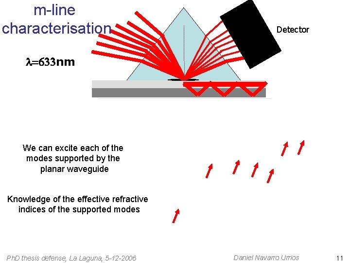
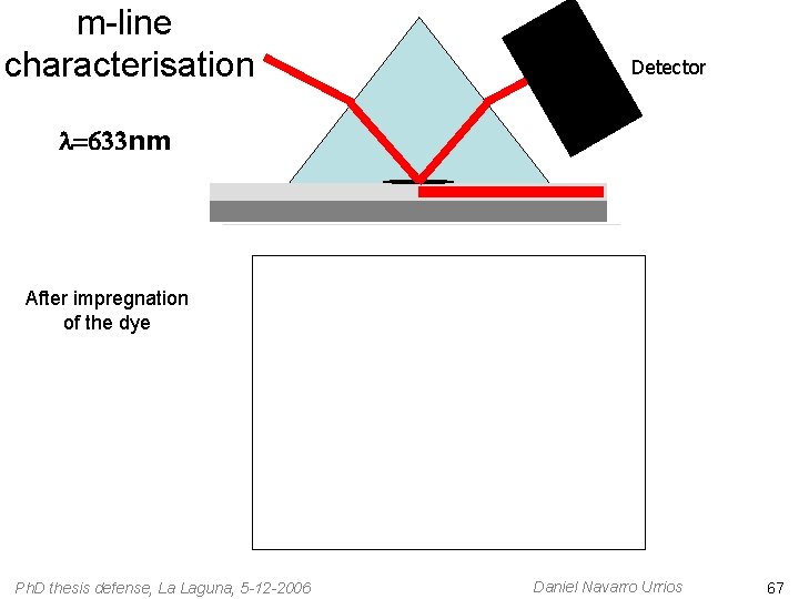
m-line characterisation Detector l=633 nm We can excite each of the modes supported by the planar waveguide Knowledge of the effective refractive indices of the supported modes Ph. D thesis defense, La Laguna, 5 -12 -2006 Daniel Navarro Urrios 11
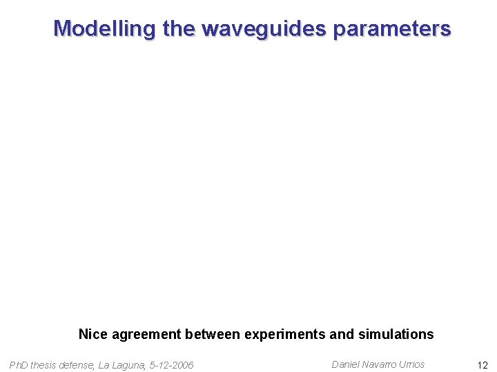
Modelling the waveguides parameters Nice agreement between experiments and simulations Ph. D thesis defense, La Laguna, 5 -12 -2006 Daniel Navarro Urrios 12
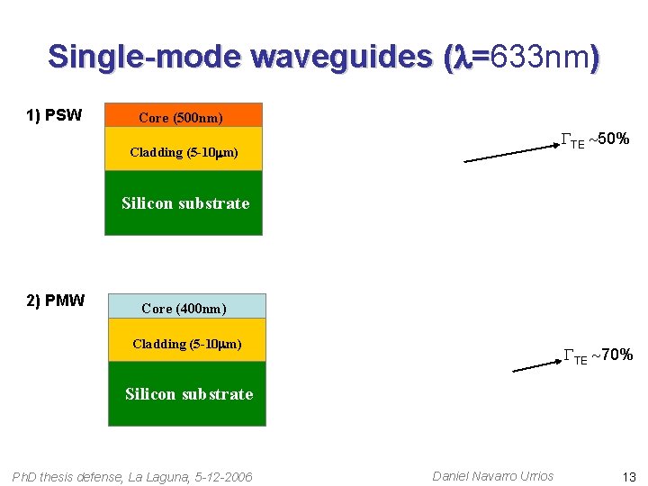
Single-mode waveguides (l=633 nm) 1) PSW Core (500 nm) TE 50% Cladding (5 -10 mm) Silicon substrate 2) PMW Core (400 nm) Cladding (5 -10 mm) TE 70% Silicon substrate Ph. D thesis defense, La Laguna, 5 -12 -2006 Daniel Navarro Urrios 13
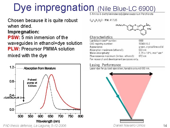
Dye impregnation (Nile Blue-LC 6900) Chosen because it is quite robust when dried. Impregnation: PSW: 5 min inmersion of the waveguides in ethanol+dye solution PLW: Precursor PMMA solution mixed with the dye Pulsed pump at 532 nm Ph. D thesis defense, La Laguna, 5 -12 -2006 Daniel Navarro Urrios 14
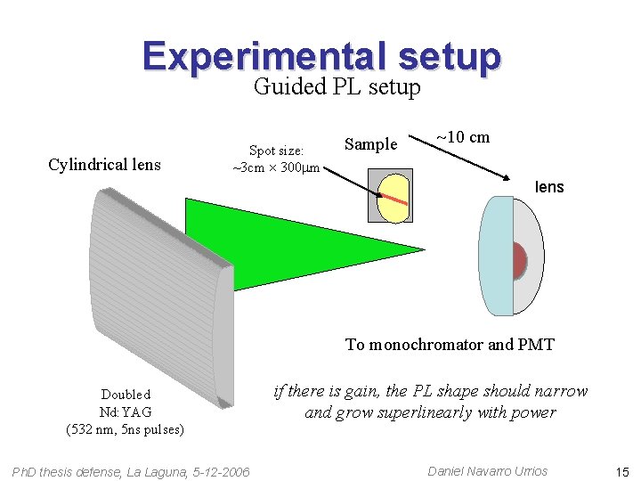
Experimental setup Guided PL setup Cylindrical lens Spot size: ~3 cm 300 m Sample 10 cm lens To monochromator and PMT Doubled Nd: YAG (532 nm, 5 ns pulses) Ph. D thesis defense, La Laguna, 5 -12 -2006 if there is gain, the PL shape should narrow and grow superlinearly with power Daniel Navarro Urrios 15
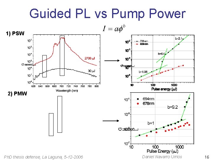
Guided PL vs Pump Power 1) PSW 2) PMW Ph. D thesis defense, La Laguna, 5 -12 -2006 Daniel Navarro Urrios 16
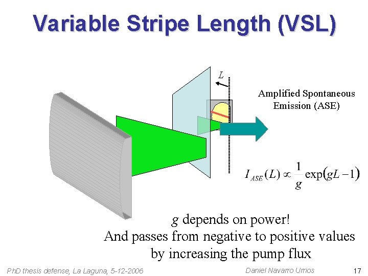
Variable Stripe Length (VSL) L Amplified Spontaneous Emission (ASE) g depends on power! And passes from negative to positive values by increasing the pump flux Ph. D thesis defense, La Laguna, 5 -12 -2006 Daniel Navarro Urrios 17
Guided PL vs Pump Power 1) PSW 2) PMW Net optical gain has been observed in both cases Ph. D thesis defense, La Laguna, 5 -12 -2006 Daniel Navarro Urrios 18
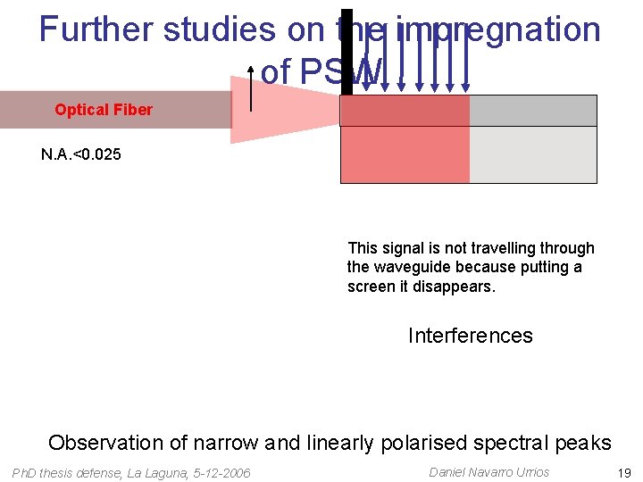
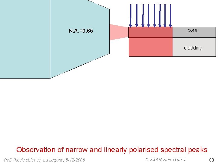
Further studies on the impregnation of PSW Optical Fiber N. A. <0. 025 This signal is not travelling through the waveguide because putting a screen it disappears. Interferences Observation of narrow and linearly polarised spectral peaks Ph. D thesis defense, La Laguna, 5 -12 -2006 Daniel Navarro Urrios 19
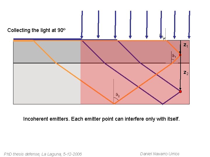
Collecting the light at 90º 0 z 1 1 z 2 2 Incoherent emitters. Each emitter point can interfere only with itself. Ph. D thesis defense, La Laguna, 5 -12 -2006 Daniel Navarro Urrios
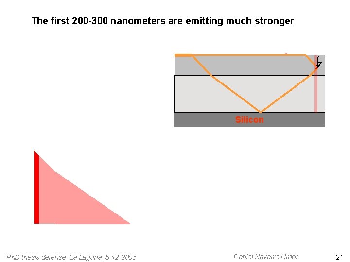
The first 200 -300 nanometers are emitting much stronger z Silicon Ph. D thesis defense, La Laguna, 5 -12 -2006 Daniel Navarro Urrios 21
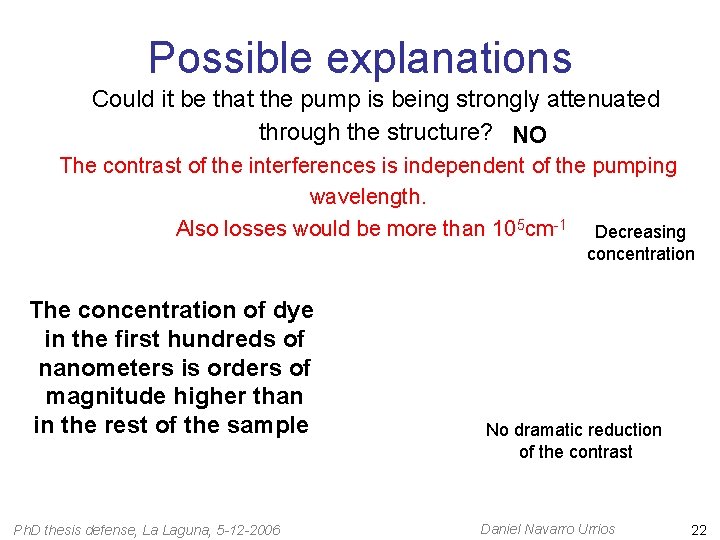
Possible explanations Could it be that the pump is being strongly attenuated through the structure? NO The contrast of the interferences is independent of the pumping wavelength. Also losses would be more than 105 cm-1 Decreasing concentration The concentration of dye in the first hundreds of nanometers is orders of magnitude higher than in the rest of the sample Ph. D thesis defense, La Laguna, 5 -12 -2006 No dramatic reduction of the contrast Daniel Navarro Urrios 22
In this kind of samples we have observed net gain in the guided configuration. We believe that the main contribution to the gain is due to these first hundreds of nanometers, because we have built micro and macro-cavities and no amplification behaviors with pump power were observed when detecting normal to the sample. Ph. D thesis defense, La Laguna, 5 -12 -2006 Daniel Navarro Urrios 23
Outline • General Introduction • Amplification studies in planar waveguides based on oxidised porous silicon • Form birefringence in Si-Nc planar waveguides • Er coupled to Si-Nc optical amplifiers • General conclusions Ph. D thesis defense, La Laguna, 5 -12 -2006 Daniel Navarro Urrios 24
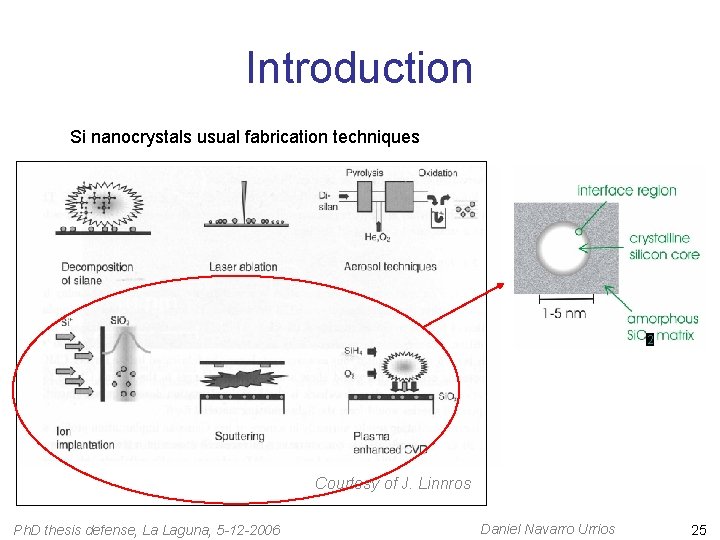
Introduction Si nanocrystals usual fabrication techniques 2 Courtesy of J. Linnros Ph. D thesis defense, La Laguna, 5 -12 -2006 Daniel Navarro Urrios 25
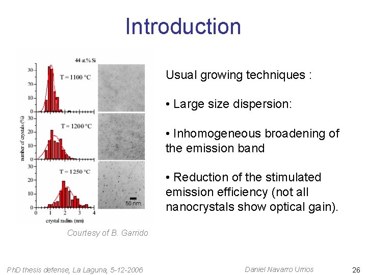
Introduction Usual growing techniques : • Large size dispersion: • Inhomogeneous broadening of the emission band • Reduction of the stimulated emission efficiency (not all nanocrystals show optical gain). Courtesy of B. Garrido Ph. D thesis defense, La Laguna, 5 -12 -2006 Daniel Navarro Urrios 26
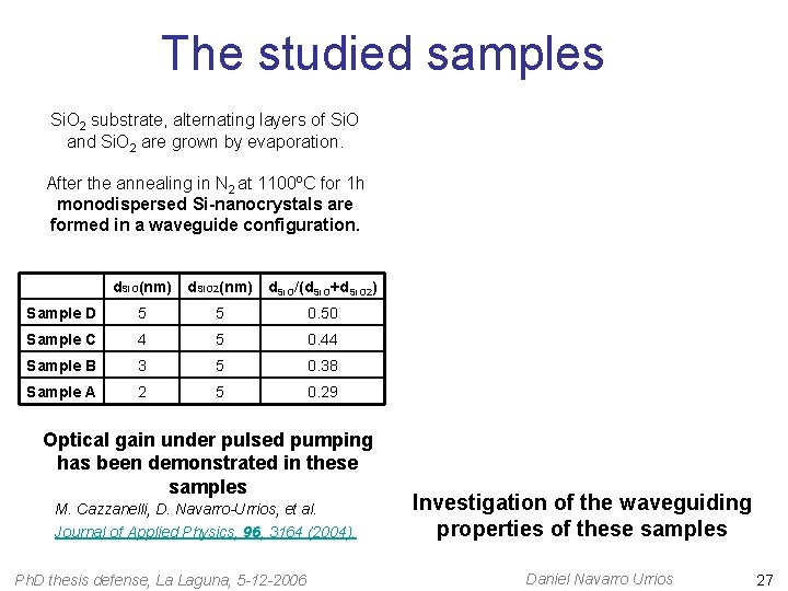
The studied samples Si. O 2 substrate, alternating layers of Si. O and Si. O 2 are grown by evaporation. After the annealing in N 2 at 1100ºC for 1 h monodispersed Si-nanocrystals are formed in a waveguide configuration. d. Si. O(nm) d. Si. O 2(nm) d. Si. O/(d. Si. O+d. Si. O 2) Sample D 5 5 0. 50 Sample C 4 5 0. 44 Sample B 3 5 0. 38 Sample A 2 5 0. 29 Optical gain under pulsed pumping has been demonstrated in these samples M. Cazzanelli, D. Navarro-Urrios, et al. Journal of Applied Physics, 96, 3164 (2004). Ph. D thesis defense, La Laguna, 5 -12 -2006 Investigation of the waveguiding properties of these samples Daniel Navarro Urrios 27
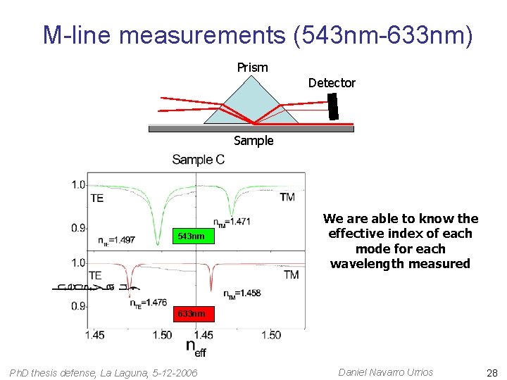
M-line measurements (543 nm-633 nm) Prism Detector Sample 543 nm We are able to know the effective index of each mode for each wavelength measured 633 nm Ph. D thesis defense, La Laguna, 5 -12 -2006 Daniel Navarro Urrios 28
Information extracted from m-line, TEM images and mode solver simulations -Thicknesses and number of periods of the SL (TEM images) -Dimension of each period (TEM images) -Effective modal indices (m-line) Material refractive indices (simulations) Ph. D thesis defense, La Laguna, 5 -12 -2006 Daniel Navarro Urrios 29
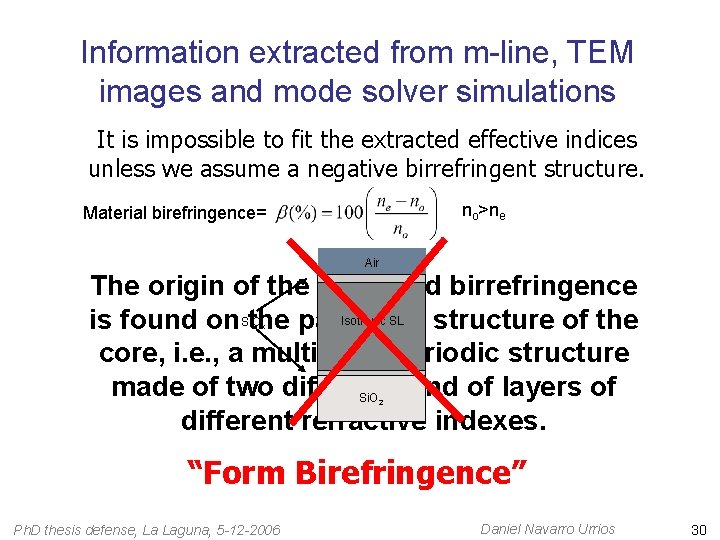
Information extracted from m-line, TEM images and mode solver simulations It is impossible to fit the extracted effective indices unless we assume a negative birrefringent structure. no>ne Material birefringence= Air The origin of the observed birrefringence Isotropic SL is found on. Si. Othe particular structure of the core, i. e. , a multilayer periodic structure made of two different kind of layers of Si. O different refractive indexes. x 2 “Form Birefringence” Ph. D thesis defense, La Laguna, 5 -12 -2006 Daniel Navarro Urrios 30
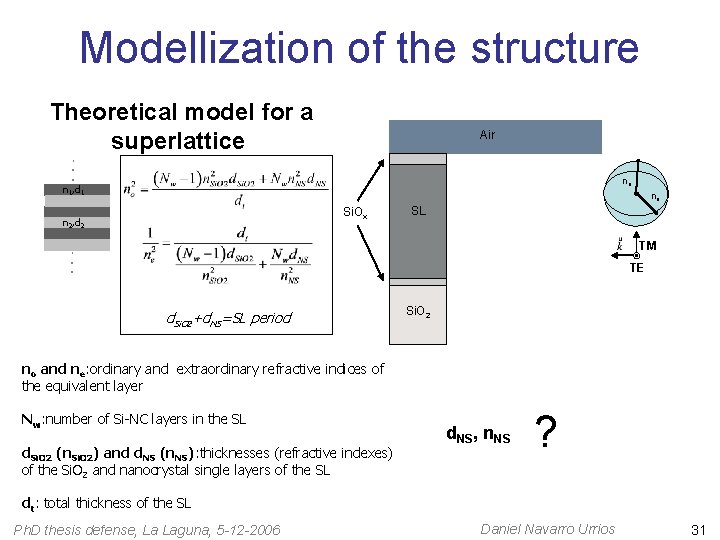
Modellization of the structure Theoretical model for a superlattice Air . . . no n 1, d 1 ne Si. Ox n 2, d 2 SL TM . . . TE d. Si. O 2+d. NS=SL period Si. O 2 no and ne: ordinary and extraordinary refractive indices of the equivalent layer Nw: number of Si-NC layers in the SL d. Si. O 2 (n. Si. O 2) and d. NS (n. NS): thicknesses (refractive indexes) of the Si. O 2 and nanocrystal single layers of the SL d. NS, n. NS ? dt: total thickness of the SL Ph. D thesis defense, La Laguna, 5 -12 -2006 Daniel Navarro Urrios 31
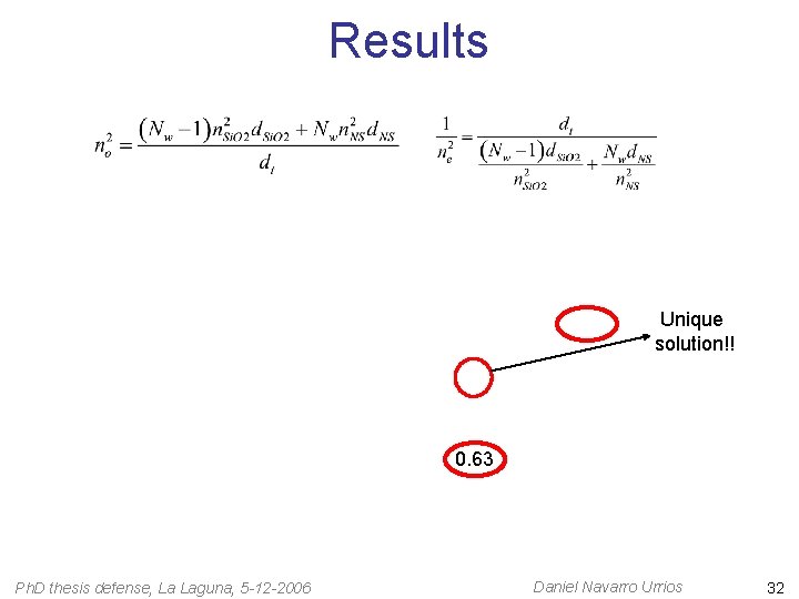
Results Unique solution!! 0. 63 Ph. D thesis defense, La Laguna, 5 -12 -2006 Daniel Navarro Urrios 32
Results Waveguide B Waveguide C Waveguide D 633 nm 543 nm n. TE 1. 462± 0. 001 1. 473± 0. 001 1. 476± 0. 001 1. 497± 0. 001 1. 519± 0. 001 1. 553± 0. 001 n. TM 1. 456± 0. 002 1. 463± 0. 001 1. 458± 0. 001 1. 471± 0. 001 1. 486± 0. 001 1. 518± 0. 001 B 0. 006± 0. 003 0. 010± 0. 002 0. 018± 0. 002 0. 026± 0. 002 0. 033± 0. 002 0. 035± 0. 002 GTE(%) 27 42 44 59 72 81 GTM(%) 3 23 10 35 56 73 n. Si. Ox 1. 4755 1. 4790 no 1. 564± 0. 003 1. 568± 0. 002 1. 600± 0. 002 1. 611± 0. 002 1. 621± 0. 001 1. 643± 0. 001 ne - 1. 567± 0. 005 1. 581± 0. 004 1. 596± 0. 002 1. 603± 0. 001 1. 624± 0. 001 b(%) - -0. 5± 0. 5 -1. 1± 0. 3 -1. 0± 0. 3 -1. 1± 0. 1 d. NS - 2. 2± 0. 3 nm 3. 1± 0. 2 nm 3. 3± 0. 1 nm 4. 4± 0. 1 nm n. NS(633 nm)= 1. 705 n. NS(543 nm)= 1. 735 Independent calculations …but the same d. NS (independent of l) Ph. D thesis defense, La Laguna, 5 -12 -2006 Daniel Navarro Urrios 33
Other studied samples Similar samples growed by sputtering technique showed similar results N. Daldosso et al. , Journal of Luminescence, 121, 2, 2006 Ion implanted samples with random distributed nanocrystals gave isotropic behavior no=ne 50 nm Ph. D thesis defense, La Laguna, 5 -12 -2006 Daniel Navarro Urrios 34
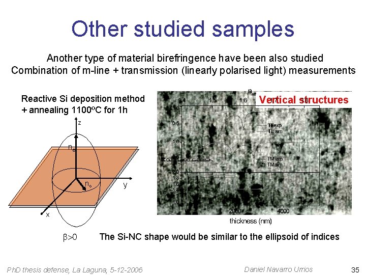
Other studied samples Another type of material birefringence have been also studied Combination of m-line + transmission (linearly polarised light) measurements Reactive Si deposition method + annealing 1100ºC for 1 h Vertical structures z ne no y x b>0 The Si-NC shape would be similar to the ellipsoid of indices Ph. D thesis defense, La Laguna, 5 -12 -2006 Daniel Navarro Urrios 35
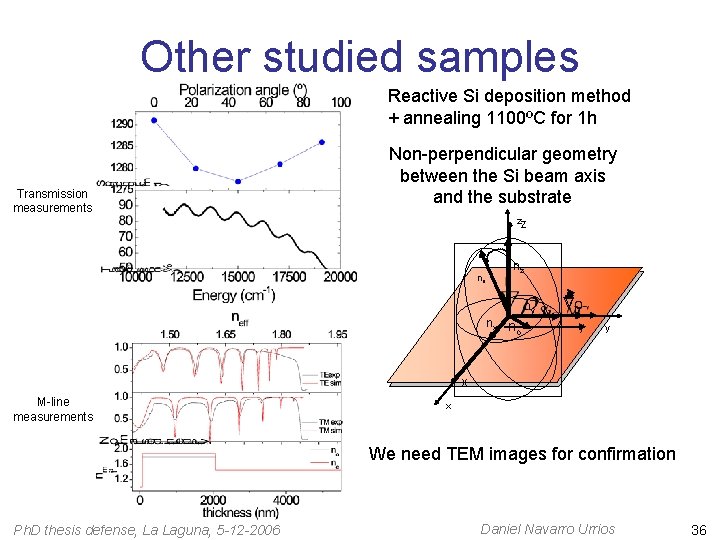
Other studied samples Reactive Si deposition method + annealing 1100ºC for 1 h Transmission measurements Non-perpendicular geometry between the Si beam axis and the substrate zz ne nz ny nx n o y y x M-line measurements x We need TEM images for confirmation Ph. D thesis defense, La Laguna, 5 -12 -2006 Daniel Navarro Urrios 36
Outline • General Introduction • Amplification studies in planar waveguides based on oxidised porous silicon • Form birefringence in Si-Nc planar waveguides • Er coupled to Si-Nc optical amplifiers • General conclusions Ph. D thesis defense, La Laguna, 5 -12 -2006 Daniel Navarro Urrios 37
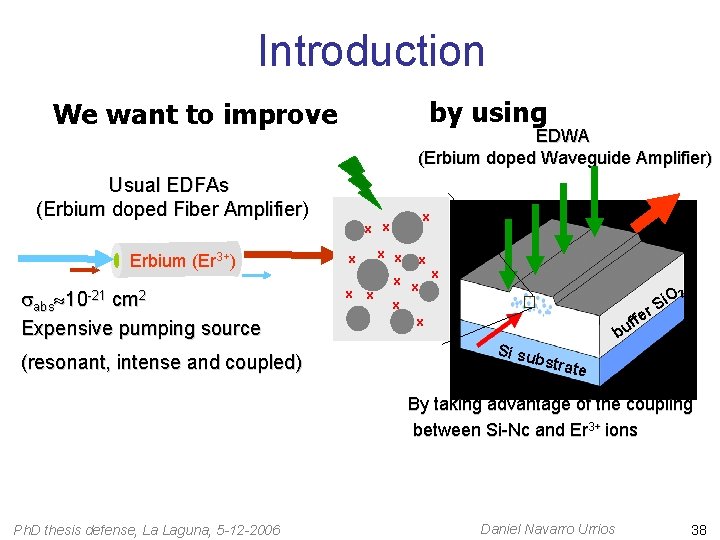
Introduction by using We want to improve EDWA (Erbium doped Waveguide Amplifier) Usual EDFAs (Erbium doped Fiber Amplifier) Erbium (Er 3+) abs 10 -21 cm 2 Expensive pumping source (resonant, intense and coupled) x x x x x x O 2 i r. S x x ffe u b x x Si su bstra t e By taking advantage of the coupling between Si-Nc and Er 3+ ions Ph. D thesis defense, La Laguna, 5 -12 -2006 Daniel Navarro Urrios 38
Why Si-Nc? Broad band absorption (UV-VIS) Increment of excitation for Er 3+ : exc from ~10 -21 (in Si. O 2) to 10 -16 -10 -18 cm 2 (with Si. Nc) Fast (~ 1 s) and efficient (~55%) energy transfer from Si-nc to Er 3+ Possibility of electrical pumping Higher index contrast for light confinement CMOS compatibility Ph. D thesis defense, La Laguna, 5 -12 -2006 Daniel Navarro Urrios 39
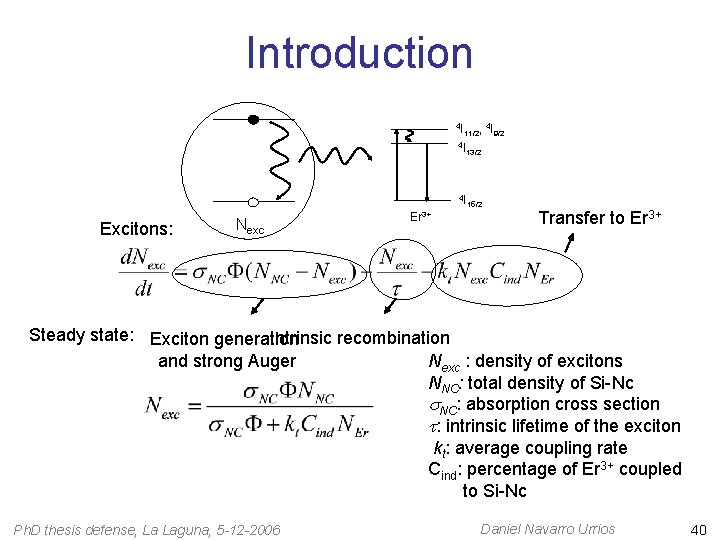
Introduction 4 I 4 11/2, I 9/2 4 I 13/2 4 I Excitons: Nexc Er 3+ 15/2 Transfer to Er 3+ Steady state: Exciton generation Intrinsic recombination and strong Auger Nexc : density of excitons NNC: total density of Si-Nc NC: absorption cross section : intrinsic lifetime of the exciton kt: average coupling rate Cind: percentage of Er 3+ coupled to Si-Nc Ph. D thesis defense, La Laguna, 5 -12 -2006 Daniel Navarro Urrios 40
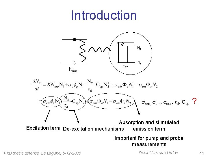
Introduction N 2 N 1 Nexc Er 3+ abs, em, exc, td, Cup ? Absorption and stimulated Excitation term De-excitation mechanisms emission term Important for pump and probe measurements Ph. D thesis defense, La Laguna, 5 -12 -2006 Daniel Navarro Urrios 41
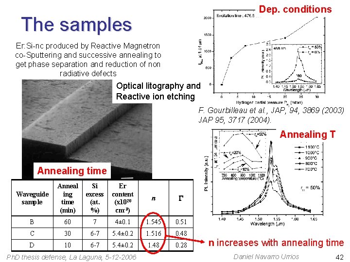
Dep. conditions The samples Er: Si-nc produced by Reactive Magnetron co-Sputtering and successive annealing to get phase separation and reduction of non radiative defects (2÷ 6 mm) Si. O 2 Optical litography and Reactive ion etching F. Gourbilleau et al. , JAP, 94, 3869 (2003) JAP 95, 3717 (2004). 800 nm Annealing T Si-nc doped Er 3+(1 mm) Si. O 2 (15 mm) Annealing time Waveguide sample Anneal Si Er Si-substrate ing excess content time (at. (x 1020 (min) %) cm-3) n G B 60 7 4± 0. 1 1. 545 0. 51 C 30 6 -7 5. 4± 0. 2 1. 516 0. 48 D 10 6 -7 5. 4± 0. 2 1. 48 0. 28 Ph. D thesis defense, La Laguna, 5 -12 -2006 n increases with annealing time Daniel Navarro Urrios 42
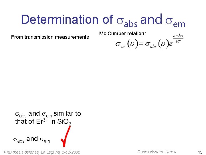
Determination of abs and em From transmission measurements Mc Cumber relation: abs and em similar to that of Er 3+ in Si. O 2 abs and em Ph. D thesis defense, La Laguna, 5 -12 -2006 Daniel Navarro Urrios 43
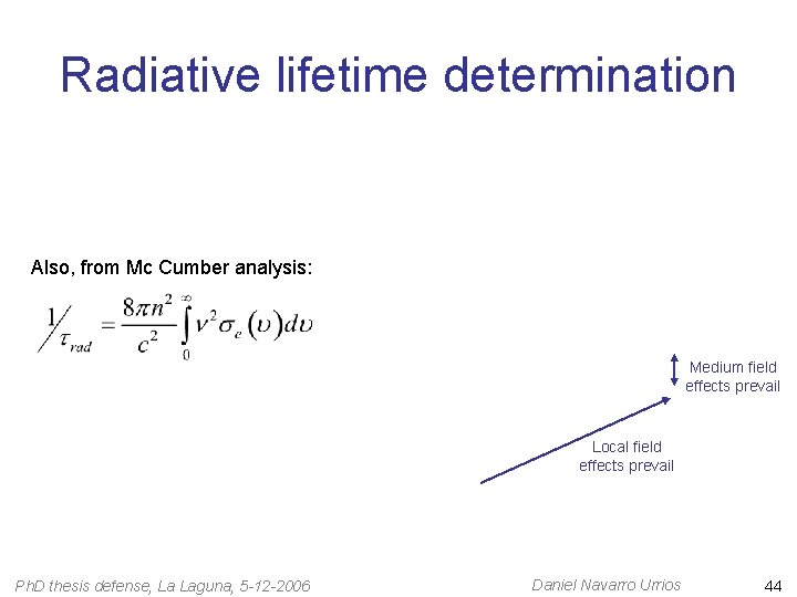
Radiative lifetime determination Also, from Mc Cumber analysis: Medium field effects prevail Local field effects prevail Ph. D thesis defense, La Laguna, 5 -12 -2006 Daniel Navarro Urrios 44
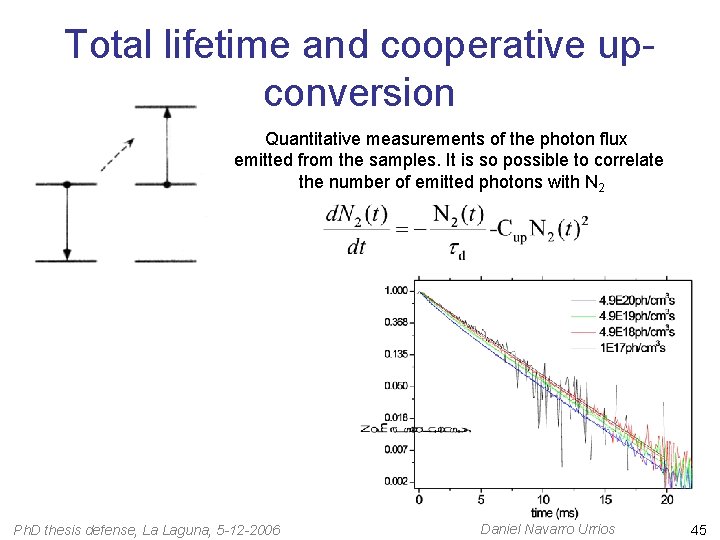
Total lifetime and cooperative upconversion Quantitative measurements of the photon flux emitted from the samples. It is so possible to correlate the number of emitted photons with N 2 Ph. D thesis defense, La Laguna, 5 -12 -2006 Daniel Navarro Urrios 45
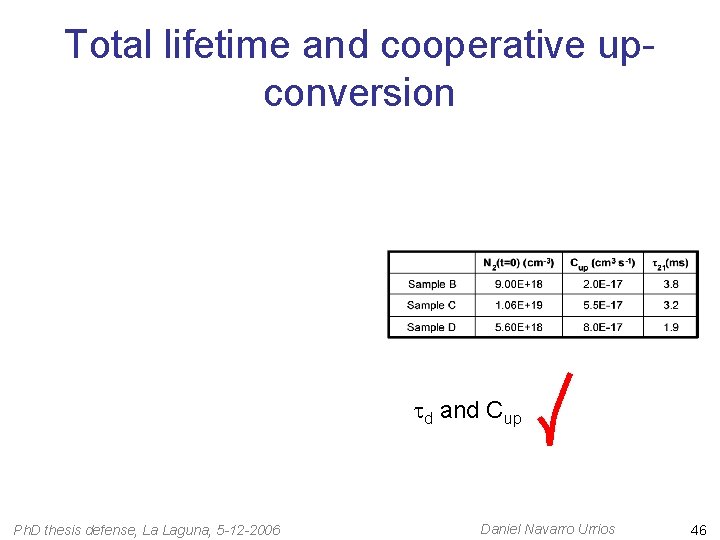
Total lifetime and cooperative upconversion td and Cup Ph. D thesis defense, La Laguna, 5 -12 -2006 Daniel Navarro Urrios 46
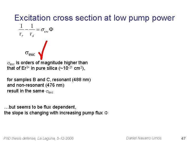
Excitation cross section at low pump power exc is orders of magnitude higher than that of Er 3+ in pure silica (~10 -21 cm 2), for samples B and C, resonant (488 nm) and non-resonant (476 nm) result in the same exc …but seems to be flux dependent, the slope is changing with increasing pump flux Ph. D thesis defense, La Laguna, 5 -12 -2006 Daniel Navarro Urrios 47
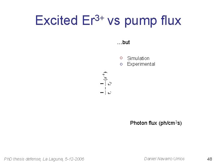
Excited Er 3+ vs pump flux …but Simulation Experimental Photon flux (ph/cm 2 s) Ph. D thesis defense, La Laguna, 5 -12 -2006 Daniel Navarro Urrios 48
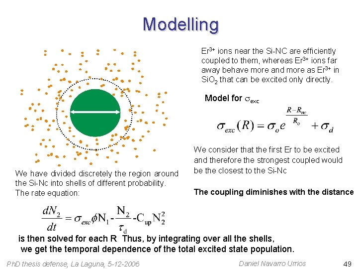
Modelling Er 3+ ions near the Si-NC are efficiently coupled to them, whereas Er 3+ ions far away behave more and more as Er 3+ in Si. O 2 that can be excited only directly. Model for exc We have divided discretely the region around the Si-Nc into shells of different probability. The rate equation: We consider that the first Er to be excited and therefore the strongest coupled would be the closest to the Si-Nc The coupling diminishes with the distance is then solved for each R Thus, by integrating over all the shells, we get the temporal dependence of the total excited state population. Ph. D thesis defense, La Laguna, 5 -12 -2006 Daniel Navarro Urrios 49
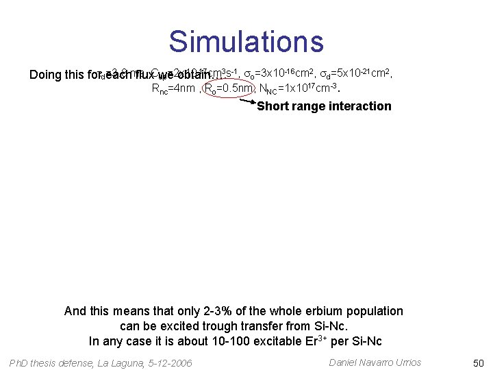
Simulations td=3. 8 ms, Cup=2 x 10 -17 cm 3 s-1, o=3 x 10 -16 cm 2, d=5 x 10 -21 cm 2, Doing this for each flux we obtain…. Rnc=4 nm , Ro=0. 5 nm, NNC=1 x 1017 cm-3. Short range interaction And this means that only 2 -3% of the whole erbium population can be excited trough transfer from Si-Nc. In any case it is about 10 -100 excitable Er 3+ per Si-Nc Ph. D thesis defense, La Laguna, 5 -12 -2006 Daniel Navarro Urrios 50
• Around 96% of the total volume of the sample is occupied by Er 3+ that are only excitable through direct photon excitation, because simply they are too far from a Si. Nc. Ph. D thesis defense, La Laguna, 5 -12 -2006 Daniel Navarro Urrios 51
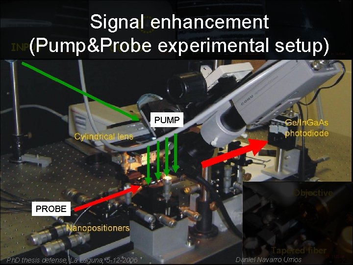
Signal enhancement INPUT OUTPUT (Pump&Probe experimental setup) PUMP PROBE Ph. D thesis defense, La Laguna, 5 -12 -2006 Daniel Navarro Urrios 52
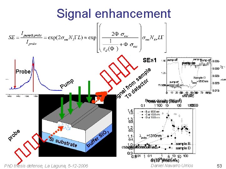
Signal enhancement SE 1 SE>1 e l p m sa tor om tec r f l de a gn To i S Probe mp u P e b ro p r Si su bstra te Ph. D thesis defense, La Laguna, 5 -12 -2006 fe uf O 2 i S b Daniel Navarro Urrios 53
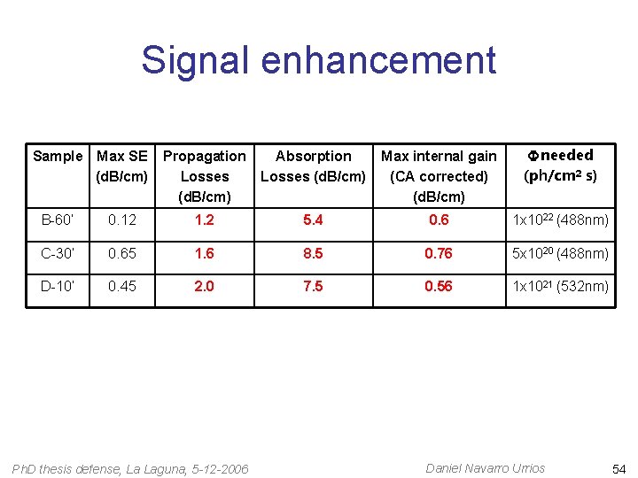
Signal enhancement Sample Max SE (d. B/cm) Propagation Losses (d. B/cm) Absorption Losses (d. B/cm) Max internal gain (CA corrected) (d. B/cm) F needed (ph/cm 2 s) B-60’ 0. 12 1. 2 5. 4 0. 6 1 x 10²² (488 nm) C-30’ 0. 65 1. 6 8. 5 0. 76 5 x 10²⁰ (488 nm) D-10’ 0. 45 2. 0 7. 5 0. 56 1 x 10²¹ (532 nm) Ph. D thesis defense, La Laguna, 5 -12 -2006 Daniel Navarro Urrios 54
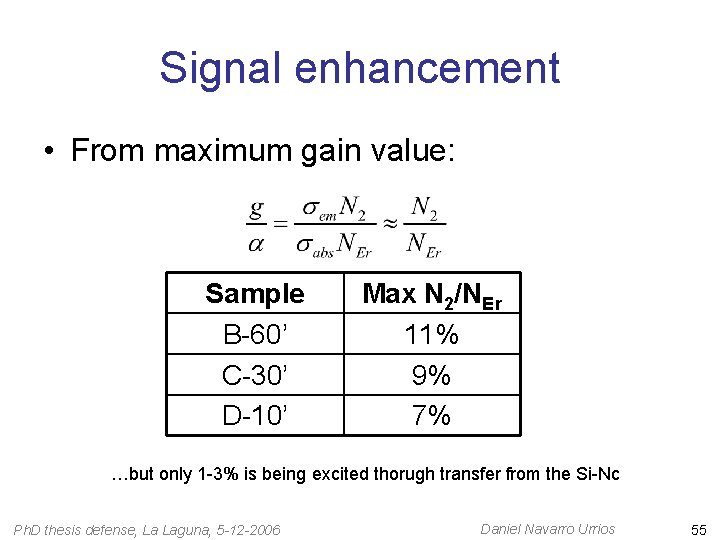
Signal enhancement • From maximum gain value: Sample B-60’ C-30’ D-10’ Max N 2/NEr 11% 9% 7% …but only 1 -3% is being excited thorugh transfer from the Si-Nc Ph. D thesis defense, La Laguna, 5 -12 -2006 Daniel Navarro Urrios 55
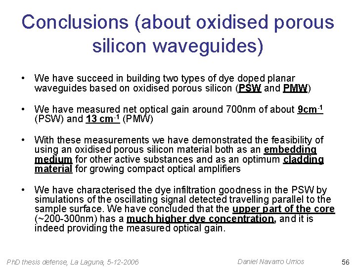
Conclusions (about oxidised porous silicon waveguides) • We have succeed in building two types of dye doped planar waveguides based on oxidised porous silicon (PSW and PMW) • We have measured net optical gain around 700 nm of about 9 cm-1 (PSW) and 13 cm-1 (PMW) • With these measurements we have demonstrated the feasibility of using an oxidised porous silicon material both as an embedding medium for other active substances and as an optimum cladding material for growing compact optical amplifiers • We have characterised the dye infiltration goodness in the PSW by simulations of the oscillating signal detected travelling parallel to the sample surface. We have concluded that the upper part of the core (~200 -300 nm) has a much higher dye concentration, and it is indeed providing the measured optical gain. Ph. D thesis defense, La Laguna, 5 -12 -2006 Daniel Navarro Urrios 56
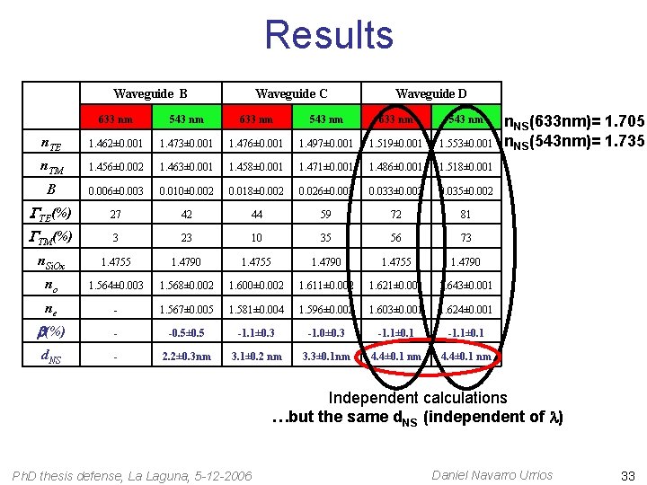
Conclusions (about birefringence in Si-Nc planar waveguides) • We have reported for the first time form birefringence phenomena in Si. Nc planar waveguides. • In the case of the multilayer structures, we were able to simulate the experimental data with a theoretical model of parallel layers of different refractive indices. • With this model, we have been able to evaluate different parameters (no, ne, n. NS) and to make an upper limit estimation of the nanocrystals diameter (d. NS), which is in good agreement with nominal growing parameters and PL spectra. Ph. D thesis defense, La Laguna, 5 -12 -2006 Daniel Navarro Urrios 57
Conclusions (about Er coupled to Si -Nc optical amplifiers) • We have measured and quantified reliable values for: Absorption and emission cross sections Total lifetimes and cooperative up-conversion coefficients Effective excitation cross sections at low pump power Indirectly excitable Er 3+ population through Si-Nc energy transfer (2 -3% of the Er 3+ concentration) • Using a pump and probe technique we have demonstrated values of internal gains of around 0. 6 d. B/cm We still have to optimize the Si-Nc: Er 3+ ratio and the characteristics of the Si-Nc in order to excite the whole Er population through indirect energy transfer Ph. D thesis defense, La Laguna, 5 -12 -2006 Daniel Navarro Urrios 58
Publications In scientific journals: 16. N. Daldosso, D. Navarro-Urrios, M. Melchiorri, C. García, P. Pellegrino, B. 1. D. Navarro-Urrios, M. Melchiorri, N. Daldosso, L. Pavesi, C. García, P. Pellegrino, B. Garrido, G. Pucker, F. Gourbilleau and R. Rizk, “Optical losses and gain in silicon-rich Silica waveguides containing Er ions”, Journal of Luminescence, 121 249– 255 (2006). 2. B. Garrido, C. García, P. Pellegrino, D. Navarro-Urrios, N. Daldosso, L. Pavesi, F. Gourbilleau, R. Rizk, “Distance dependent interaction as the limiting factor for Si nanocluster to Er energy transfer in silica”, Applied Physics Letters, 89, 163103 (2006). 3. C. J. Oton, D. Navarro-Urrios, N. E. Capuj, M. Ghulinyan, L. Pavesi, S. González-Pérez, F. Lahoz, and I. R. Martín, “Optical gain in dye-impregnated oxidized porous silicon waveguides”, Applied Physics Letters, 89, 011107 (2006). 4. N. Daldosso, D. Navarro-Urrios, M. Melchiorri, L. Pavesi, C. Sada, F. Gourbilleau and R. Rizk, “Refractive index dependence of the absorption and emission cross sections at 1. 54 m m of Er 3+ coupled to Si nanoclusters”, Applied Physics Letters, 88, 161901 (2006). 5. K. Luterová , M. Cazzanelli, J. -P. Likforman , D. Navarro-Urrios, J. Valenta, T. Ostatnický, K. Dohnalová, S. Cheylan, P. Gilliot, B. Hönerlage, L. Pavesi, I. Pelant, “Optical gain in nanocrystalline silicon: comparison of planar waveguide geometry with a non-waveguiding ensemble of nanocrystals”, Optical Materials 27, 750– 755 (2005). 6. K. Luterová, D. Navarro-Urrios, M. Cazzanelli, T. Ostatnický, J. Valenta, S. Cheylan, I. Pelant, and L. Pavesi, “Stimulated emission in the active planar optical waveguide made of silicon nanocrystals”, phys. stat. solidi (c), 2, No. 9, 3429 -3434 (2005). 7. D. Navarro-Urrios, C. Pérez-Padrón, E. Lorenzo, N. E. Capuj, Z. Gaburro, C. J. Oton and L. Pavesi, “Structural and light-emission modification in chemically post-etched porous silicon”, phys. stat. sol. (a) 202, No. 8, 1518– 1523 (2005). 8. E. Lorenzo-Cabrera, C. J. Oton, N. E. Capuj, M. Ghulinyan, D. Navarro-Urrios, Z. Gaburro, L. Pavesi, “Fabrication and optimization of rugate filters based on porous silicon”, phys. stat. sol. (c) 2, No. 9, 3227– 3231 (2005). 9. V. Venkatramu, D. Navarro-Urrios, P. Babu, C. K. Jayasankar , V. Lavín, “Fluorescence line narrowing spectral studies of Eu 3+-doped lead borate glass”, Journal of Non. Crystalline Solids 351, 929– 935 (2005). 10. E. Lorenzo, C. J. Oton, N. E. Capuj, M. Ghulinyan, D. Navarro-Urrios, Z. Gaburro, L. Pavesi “Porous silicon-based rugate filters”, Applied Optics, 44, 26 (2005). 11. D. Navarro-Urrios, F. Riboli, M. Cazzanelli, A. Chiasera, N. Daldosso, L. Pavesi, C. J. Oton, J. Heitmann, L. X. Yi, R. Scholz and M. Zacharias, “Birefingence characterization of mono-dispersed silicon nanocrystals planar waveguides”Optical Materials 27 (5) pp. 763 -768 (2005). 12. N. Daldosso, D. Navarro-Urrios, M. Melchiorri, and L. Pavesi, F. Gourbilleau, M. Carrada, R. Rizk, C. García, P. Pellegrino, B. Garrido, and L. Cognolato, “ Absorption cross section and signal enhancement in Er-doped Si-nanocluster rib-loaded waveguides”, Applied Physics Letters, 86, 261103 (2005). 13. M. Cazzanelli, D. Navarro-Urrios, F. Riboli, N. Daldosso, L. Pavesi, J. Heitmann, L. X. Yi, R. Scholz, M. Zacharias, and U. Gösele, “ Optical gain in mono-dispersed silicon nanocrystals”, Journal of Applied Physics, 96, 3164 (2004). 14. F. Riboli, D. Navarro-Urrios, A. Chiasera, N. Daldosso, L. Pavesi, C. J. Oton, J. Heitmann, L. X. Yi, R. Scholz and M. Zacharias, “Birefringence in optical waveguides made by silicon nanocrystal superlattices” Applied Physics Letters 85 (7) pp. 1268 -1270 (2004). 15. D. Navarro-Urrios, N. Daldosso, L. Pavesi, C. García, P. Pellegrino, B. Garrido, F. Gourbilleau and R. Rizk, “Signal enhancement and limiting factors in waveguides containing Si Nanoclusters and Er 3+ ions”, submitted to Journal of Lightwave Technology. Ph. D thesis defense, La Laguna, 5 -12 -2006 17. 18. 19. 20. 21. Garrido, C. Sada, G. Battaglin, F. Gourbilleau, R. Rizk, L. Pavesi, “ Er Coupled Si Nanocluster Waveguide”, to be published in IEEE- Journal of Selected Topics in Quantum Electronics. C. J. Oton, D. Navarro Urrios, M. Ghulinyan, N. E. Capuj, S. González Pérez, F. Lahoz, I. R. Martín and L. Pavesi, “ Optical gain in oxidized porous silicon waveguides impregnated with a laser dye”, accepted in Physica Status Solidi. D. Navarro-Urrios, M. Ghulinyan, N. E. Capuj, C. J. Oton, F. Riboli, I. R. Martín and L. Pavesi, “Waveguiding, absorption and emission properties of dyeimpregnated oxidized porous silicon”, submitted to Physica Status Solidi. L. Khriachtchev, D. Navarro-Urrios, L. Pavesi, C. J. Oton, N. Capuj and S. Novikov, “Cut-off and m-line spectroscopy of silica layers containing Si nanocrystals: Experimental evidence of optical birefringence”, to be published in Journal of Applied Physics. F. Lahoz, N. E. Capuj, D. Navarro-Urrios, and S. E. Hernández, "Optical amplification in Ho 3+ - doped transparent oxyfluoride glass-ceramics at 750 nm", submitted to Applied Physics Letters. D. Navarro-Urrios, M. Ghulinyan, P. Bettotti, C. J. Oton, N. E. Capuj, F. Lahoz, I. R. Martin, and L. Pavesi, "Optical gain in dye-doped polymeric slab waveguides on silicon", submitted to Applied Physics Letters. Conference proceedings: 22. C. J. Oton, E. Lorenzo, N. Capuj, F. Lahoz, I. R. Martín, D. Navarro-Urrios, M. Ghulinyan, F. Sbrana, Z. Gaburro, L. Pavesi, “Porous silicon-based Notch filters and waveguides”Proceedings of SPIE, 5840, 434 (2005). 23. Pump-probe experiments on low loss silica waveguides containing Si nanocrystals, D. Navarro-Urrios, N. Daldosso, M. Melchiorri, F. Sbrana, L. Pavesi, C. García, B. Garrido, P. Pellegrino, J. R. Morante, E. Scheid and G. Sarrabayrouse, Mater. Res. Soc. Symp. Proc. Vol. 832, F 10. 11. 1 (2005). 24. Pump-probe experiments on Er coupled Si-nanocrystals rib-loaded waveguides, N. Daldosso, D. Navarro-Urrios, M. Melchiorri, L. Pavesi, F. Gourbilleau, M. Carrada, R. Rizk, C. García, P. Pellegrino, B. Garrido, and L. Cognolato, Mater. Res. Soc. Symp. Proc. Vol. 832, F 11. 3. 1 (2005). 25. D. Navarro-Urrios, C. Pérez-Padrón, E. Lorenzo, N. E. Capuj, Z. Gaburro, C. J. Oton and L. Pavesi, “Chemical etching effects in porous silicon layers”Proceedings of SPIE, 5118 pp. 109 -115 (2003). Contributions to books: 26. “Nanostructured Silicon for Photonics - from Materials to Devices –“ , Z. Gaburro, P. Bettotti, N. Daldosso, M. Ghulinyan, D. Navarro-Urrios, M. Melchiorri, F. Riboli, M. Saiani, F. Sbrana and L. Pavesi, Materials Science Foundations, Volume 27 until 28 (2006), ISBN 0 -87849 -488 -x Daniel Navarro Urrios 59
Acknowledgements Finantial Support: • European projects SINERGIA and LANCER. • Dipartimento di Fisica della Università di Trento • Istituto Nazionale per la Fisica della Materia, INFM • Integrated Action Spain-Italy, 2004 -2006 Special acknoledgements to C. J. Otón, L. Pavesi and N. Daldosso for some slides used in this presentation and to everybody that have collaborated in this research work. Thank you! Ph. D thesis defense, La Laguna, 5 -12 -2006 Daniel Navarro Urrios 60
Ph. D thesis defense, La Laguna, 5 -12 -2006 Daniel Navarro Urrios 61
Ph. D thesis defense, La Laguna, 5 -12 -2006 Daniel Navarro Urrios 62
Silicon vs. III-V Direct band gap: efficiency • –VCSEL 50% • –LED 37%, potentially 50% – • Tunability 400 nm -10 μm you choose! – • Material and processing expensive – • Integration with CMOS devices: costly, low yield, still difficult Ph. D thesis defense, La Laguna, 5 -12 -2006 Daniel Navarro Urrios 63
Oxidised porous silicon waveguides (extra slides) Ph. D thesis defense, La Laguna, 5 -12 -2006 Daniel Navarro Urrios 64
Amplification studies in planar waveguides based on oxidised porous silicon • Dye doped oxidized porous silicon waveguides (PSW) • Dye doped polymeric waveguides with oxidized porous silicon cladding (PMW) Ph. D thesis defense, La Laguna, 5 -12 -2006 Daniel Navarro Urrios 65
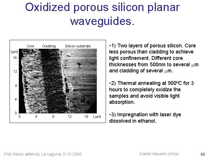
Oxidized porous silicon planar waveguides. Core Cladding Silicon substrate ( m) 16 12 • 2) Thermal annealing at 900ºC for 3 hours to completely oxidize the samples and avoid visible light absorption. 8 4 0 • 1) Two layers of porous silicon. Core less porous than cladding to achieve light confinement. Different core thicknesses from 500 nm to several m and cladding of several m. 0 4 8 12 16 ( m) Ph. D thesis defense, La Laguna, 5 -12 -2006 • 3) Impregnation with laser dye dissolved in ethanol. Daniel Navarro Urrios 66
m-line characterisation Detector l=633 nm After impregnation of the dye Ph. D thesis defense, La Laguna, 5 -12 -2006 Daniel Navarro Urrios 67
core N. A. =0. 65 cladding Observation of narrow and linearly polarised spectral peaks Ph. D thesis defense, La Laguna, 5 -12 -2006 Daniel Navarro Urrios 68
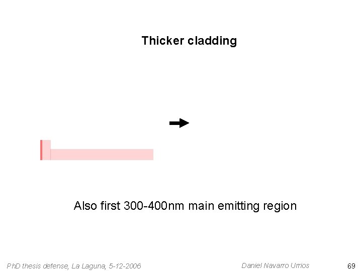
Thicker cladding Also first 300 -400 nm main emitting region Ph. D thesis defense, La Laguna, 5 -12 -2006 Daniel Navarro Urrios 69
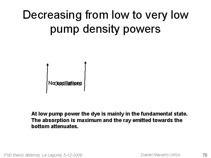
Decreasing from low to very low pump density powers No oscillations Oscillations At low pump power the dye is mainly in the fundamental state. The absorption is maximum and the ray emitted towards the bottom attenuates. Ph. D thesis defense, La Laguna, 5 -12 -2006 Daniel Navarro Urrios 70
Could it be in the surface? • We fit very well the data. • Why optical gain. If it is in the surface the overlapping with the confined mode will be very low. Ph. D thesis defense, La Laguna, 5 -12 -2006 Daniel Navarro Urrios 71
Future work SNOM characterization of the profile of dye concentration is in progress. 1 D vertical photonic crystals. We have to achieve several microns with high dye concentration if we want to arrive to an eventual microcavity or impregnate a random photonic crystal. We will decrease the porosity of the high index layer although we will loose index contrast. Ph. D thesis defense, La Laguna, 5 -12 -2006 Daniel Navarro Urrios 72
Birefringence extra slides Ph. D thesis defense, La Laguna, 5 -12 -2006 Daniel Navarro Urrios 73
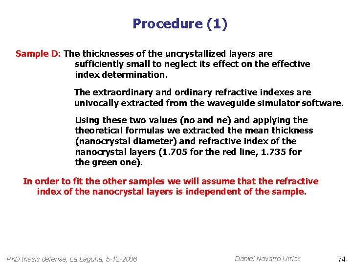
Procedure (1) Sample D: The thicknesses of the uncrystallized layers are sufficiently small to neglect its effect on the effective index determination. The extraordinary and ordinary refractive indexes are univocally extracted from the waveguide simulator software. Using these two values (no and ne) and applying theoretical formulas we extracted the mean thickness (nanocrystal diameter) and refractive index of the nanocrystal layers (1. 705 for the red line, 1. 735 for the green one). In order to fit the other samples we will assume that the refractive index of the nanocrystal layers is independent of the sample. Ph. D thesis defense, La Laguna, 5 -12 -2006 Daniel Navarro Urrios 74
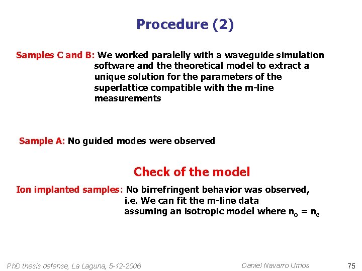
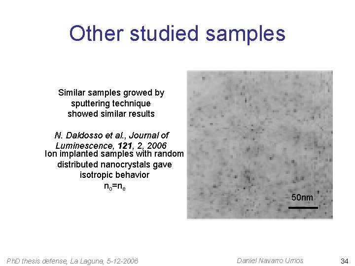
Procedure (2) Samples C and B: We worked paralelly with a waveguide simulation software and theoretical model to extract a unique solution for the parameters of the superlattice compatible with the m-line measurements Sample A: No guided modes were observed Check of the model Ion implanted samples: No birrefringent behavior was observed, i. e. We can fit the m-line data assuming an isotropic model where no = ne Ph. D thesis defense, La Laguna, 5 -12 -2006 Daniel Navarro Urrios 75
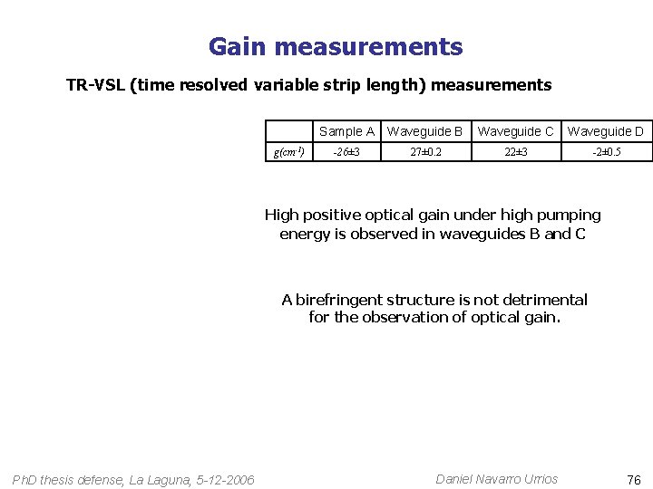
Gain measurements TR-VSL (time resolved variable strip length) measurements g(cm-1) Sample A Waveguide B Waveguide C Waveguide D -26± 3 27± 0. 2 22± 3 -2± 0. 5 High positive optical gain under high pumping energy is observed in waveguides B and C A birefringent structure is not detrimental for the observation of optical gain. Ph. D thesis defense, La Laguna, 5 -12 -2006 Daniel Navarro Urrios 76
- Slides: 76