Nuclear Instruments and Methods in Physics Research A





- Slides: 20

Nuclear Instruments and Methods in Physics Research A 436 (1999) 272 -280 Design optimization of radiation-hard, doublesided, double-metal, ACcoupled silicon sensors T. Ohsugi (Hiroshima U) K. Yamamoto (HPK) This document presented by Dong. Ha Kah in KNU

Contents 1. Introduction 2. Design rule 1. Double-metal layer 2. 3. 4. 5. 6. 7. Strip pitch and width Generals Electrode Bias resistor Guard-ring n edge filed shaper 3. Electric properties 3. leakage current 4. micro-discharge 4. Conclusion 8. Underneath of bias resistor 9. p-stop 10. Second metal layer 11. Coupling capacitor 12. Passsivation Takashi Ohsugi http: //www-heaf. hepl. hiroshima-u. ac. jp/

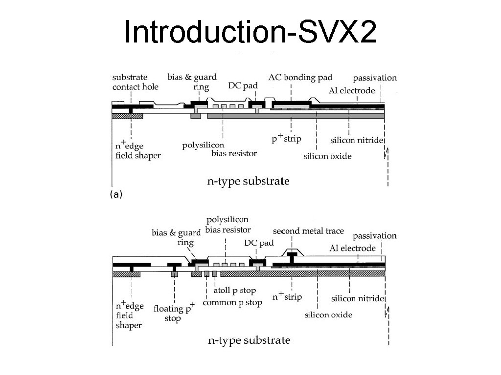
Introduction-SVX 2 � Upgrade plan of CDF vertex detector at FNAL � 5 layers • 3 layers +2 layer � Radiation hardness • 10 k. Gy(1 Mrad) over 2 years • with high bias voltage • low capacitance � micro-discharge free at high voltage Rad (radiation absorbed dose)- Measures a quantity called “absorbed dose” which means the amount of energy actually absorbed in a material. The rad measures any type of radiation, but it does not describe the biological effects.

Introduction-SVX 2

Introduction-SVX 2

Double-metal layer �The readout chips on both sides should be placed at the end of long ladder for easy integration of detector �To reduce the crossing-capacitance between two metal layers, a 5 m thick oxide deposition between the two metal traces has been implemented 8 mm 457. + 3 3 L 4 L 3 3 + 1 + 2 2 1 + 1 L 2 L 1 5 mm 156.

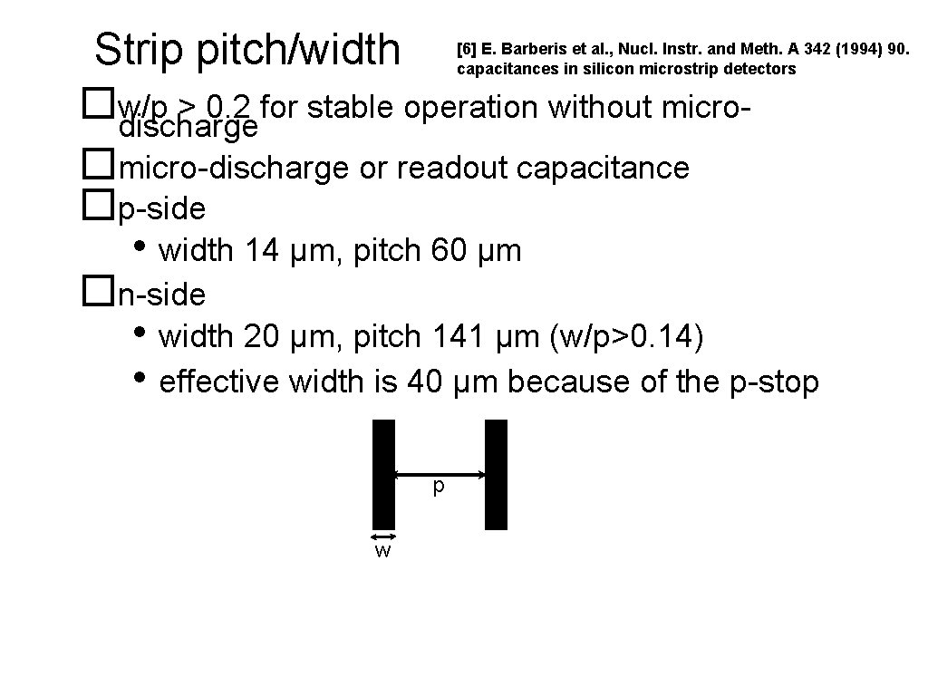
Strip pitch/width �w/p > 0. 2 for stable operation without microdischarge �micro-discharge or readout capacitance �p-side • width 14 μm, pitch 60 μm �n-side • width 20 μm, pitch 141 μm (w/p>0. 14) • effective width is 40 μm because of the p-stop [6] E. Barberis et al. , Nucl. Instr. and Meth. A 342 (1994) 90. capacitances in silicon microstrip detectors p w

Generals �To prevent micro-discharge by high electric filed • corner/edge of electrode must have radius >10 μm �Photo-mask accuracy • Any structure must have a width >10 μm �Doping concentration • Doping concentration >1014 ions/cm 2 �Contamination • specially, avoid a sodium ion • breakdown

Electrode �To achieve lower series resistance • pure Al ➛ silicon-doped Al alloy �To suppress the micro-discharge • electrode width : 8 μm, implanted strip width : 14 μm �To reduce the series resistance • electrode thickness : > 1 μm

Bias resistor �Be proved to be radiation hard • bias resistor is made with polysilicon �For sensitive area • installed over a oxide layer �Typically, • 1~4 MΩ/mm for 5 μm wide line �Uniformity and radiation hardness • high-doped polysilicon : lower sheet resistivity • variation of resistance < 5%(sensor), ± 30%(batch)

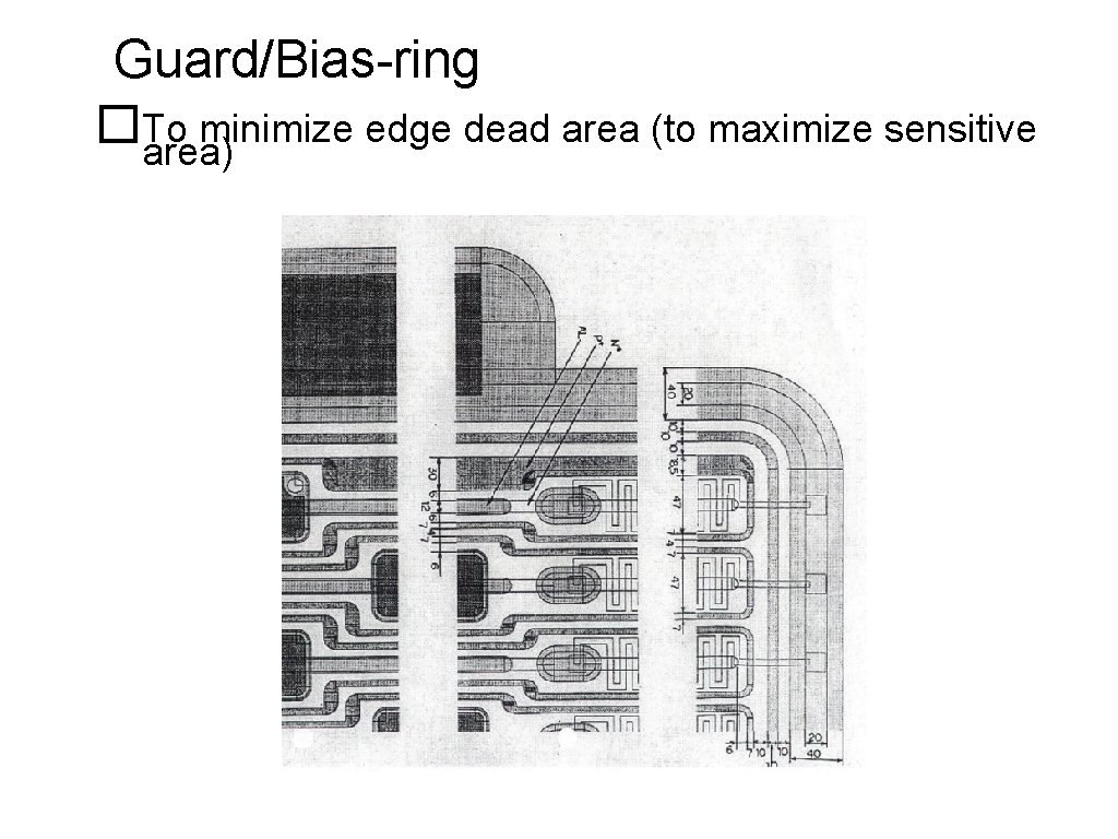
Guard/Bias-ring �To minimize edge dead area (to maximize sensitive area)

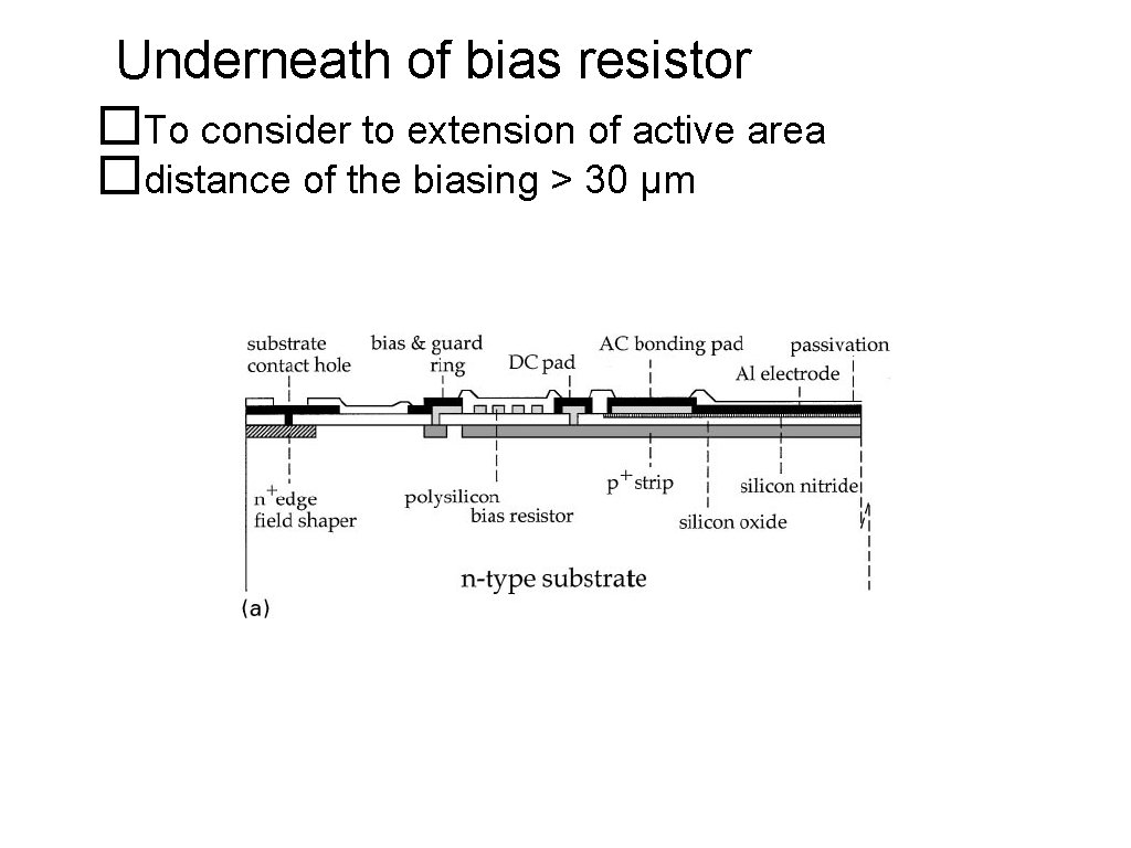
Underneath of bias resistor �To consider to extension of active area �distance of the biasing > 30 μm

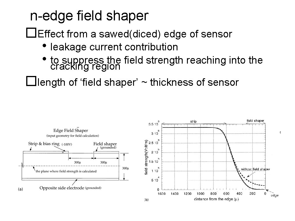
n-edge field shaper �Effect from a sawed(diced) edge of sensor • leakage current contribution • to suppress the field strength reaching into the cracking region �length of ‘field shaper’ ~ thickness of sensor

p-stop atoll/combined type �Why needs p-stop atoll patterns on n-side ? • Si-Si. O 2 interface has positive charge • electron accumulation layer • electric shorting • poor resolution • n-strips are need isolated [12] Y. Iwata et al. , IEEE Nucl. Sci. Trans. NS-45 (3) (1998) 303. [13] Y. Unno et al. , IEEE Nucl. Sci. Trans. NS-45 (3) (1988) 401.

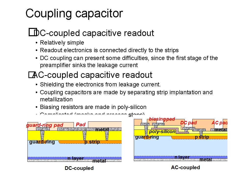
Coupling capacitor �DC-coupled capacitive readout • Relatively simple • Readout electronics is connected directly to the strips • DC coupling can present some difficulties, since the first stage of the preamplifier sinks the leakage current �AC-coupled capacitive readout • Shielding the electronics from leakage current. • Coupling capacitors are made by separating strip implantation and metallization • Biasing resistors are made in poly-silicon • Complicated (masks and process steps)

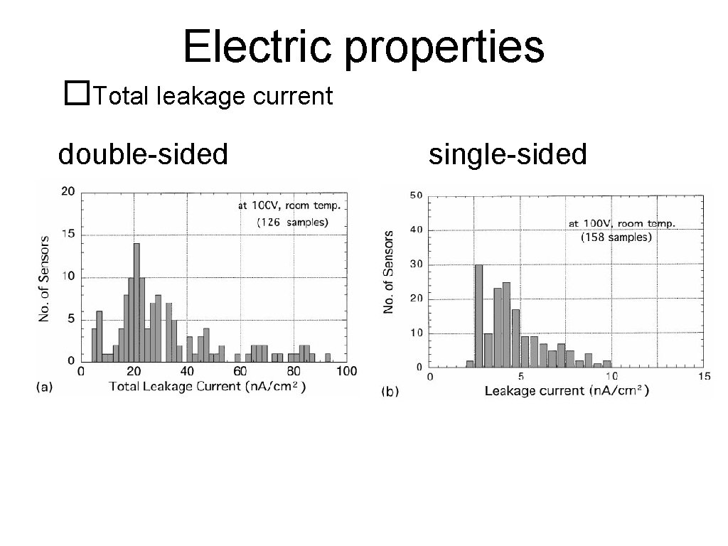
Electric properties �Total leakage current double-sided single-sided

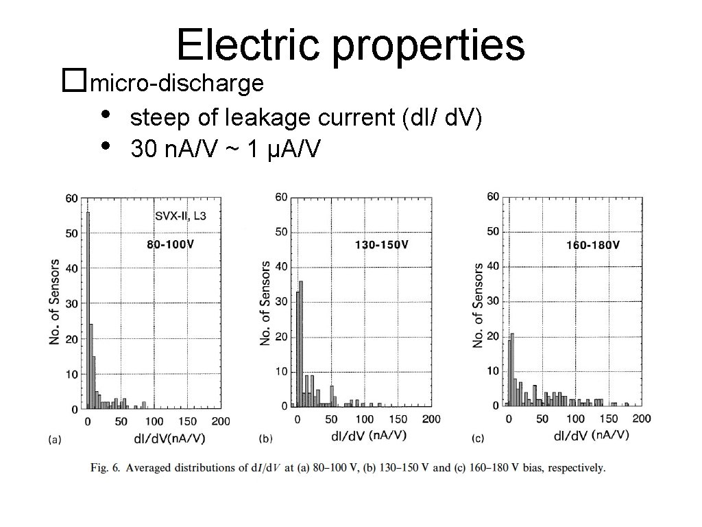
Electric properties �micro-discharge • steep of leakage current (d. I/ d. V) • 30 n. A/V ~ 1 μA/V

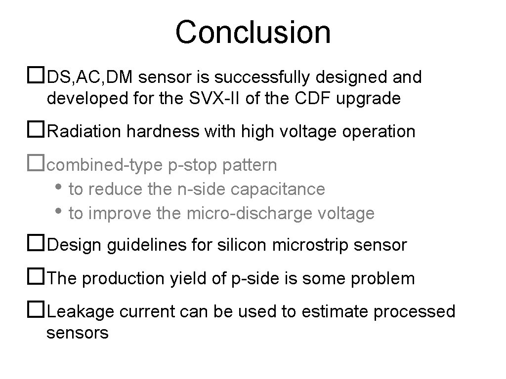
Conclusion �DS, AC, DM sensor is successfully designed and developed for the SVX-II of the CDF upgrade �Radiation hardness with high voltage operation �combined-type p-stop pattern • to reduce the n-side capacitance • to improve the micro-discharge voltage �Design guidelines for silicon microstrip sensor �The production yield of p-side is some problem �Leakage current can be used to estimate processed sensors


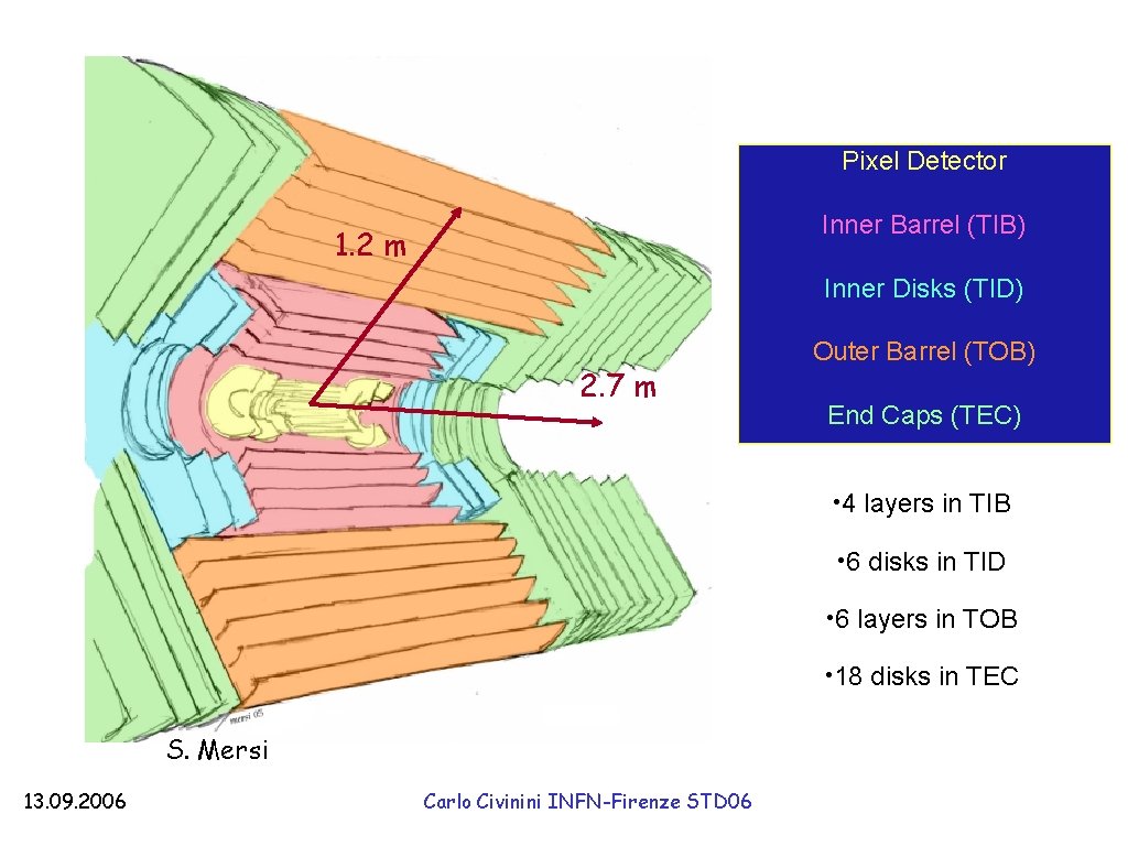
Pixel Detector Inner Barrel (TIB) 1. 2 m Inner Disks (TID) 2. 7 m Outer Barrel (TOB) End Caps (TEC) • 4 layers in TIB • 6 disks in TID • 6 layers in TOB • 18 disks in TEC S. Mersi 13. 09. 2006 Carlo Civinini INFN-Firenze STD 06