NS 9750 Training Hardware Serial Controller UART UART


- Slides: 21

NS 9750 - Training Hardware

Serial Controller - UART

UART Overview • 4 Serial Controller Channels (A, B, C, D) • External GPIO connections via TXD, RTS, CTS, DTR, DSR, DCD, RI

UART Hardware • Based upon NS 7520 Serial Controller design with minor enhancements and bug fixes. – Improved data capture and status reporting for Receive Buffer Closed conditions, for example. • Bit-Rate generation from internal or external clocking source, supporting baud rates from 75 to 1, 843, 200 (x 8 mode only) • Data support via DMA or BBus Interrupt

UART Hardware • Four 8 -bit Character Match registers • SW/HW Initiated XON/XOFF based on Character Match for Flow Control • Flow Control Force Register – to disable transmit state machine – to transmit specified Character while TX_IDLE • Error detection: – FIFO overrun, Break, Parity or Frame Errors

UART Configuration • Initialize per-channel Bit Rate Register to – Enable EBIT – Set TMODE = 1 and TCDR=RCDR (x 8, x 16, or x 32) for asynchronous operation – Set Clk. Mux to select the oscillator as the source – Set N-value for desired Baud Rate (refer to Hardware Ref. Manual) • Initialize Character Gap or Buffer Gap Timers

UART Configuration • Initialize Control Register A for – Channel Enable, Word Size, Stop Bits, Parity Enable, Break, RTS, DTR, Rx/Tx Interrupt or DMA Enables • Initialize Control Register B for – UART Mode, Char. Match, Enable Character or Buffer Gap Timers, RTS Flow Control • Initialize BBus Utility GPIO Config registers to enable desired UART interface pins

Serial Controller SPI

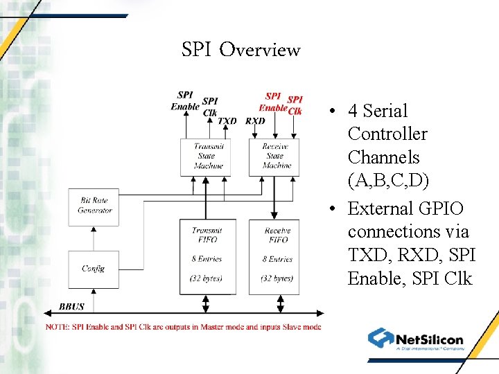
SPI Overview • 4 Serial Controller Channels (A, B, C, D) • External GPIO connections via TXD, RXD, SPI Enable, SPI Clk

SPI Hardware • Based upon NS 7520 Serial Controller design with minor enhancements and bug fixes. – All four SPI Clocking modes are functional as opposed to only Clk 0 and Clk 1 in the NS 7520, for example • Bit-Rate generation from internal or external clocking source • Data support via DMA or BBus Interrupt

SPI Hardware • Four 8 -bit Character Match registers • Flow Control Force Register – to disable transmit state machine – to transmit specified Character while TX_IDLE • Error detection: – FIFO overrun • SPI-EEPROM Boot from SDRAM following powerup (Serial Chan. A only. )

SPI Master Configuration • Initialize per-channel Bit Rate Register to – Enable EBIT – Set TMODE=1 and TCDR=RCDR=0 for synchronous (x 1) operation – Enable TXEXT to drive transmit clock via GPIOs – Set Clk. Mux to select BCLK as the source – Set SPCPOL, RXCINV, TXCINV to select the desired SPI Clock Mode (refer to Hardware Ref. Manual) – Set N-value for desired Bit Rate (refer to Hardware Ref. Manual)

SPI Master Configuration • Initialize Control Register A for – Channel Enable, Word Size, Rx/Tx Interrupt or DMA Enables • Initialize Control Register B for – SPI Master Mode, SPI Enable Polarity, Bit Order, Character Match, and Character or Buffer Gap Timers Enables • Initialize Character Gap or Buffer Gap Timers • Initialize BBus Utility GPIO Config registers to enable desired SPI Master interface pins

Serial Controller HDLC

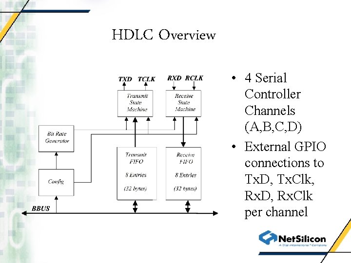
HDLC Overview • 4 Serial Controller Channels (A, B, C, D) • External GPIO connections to Tx. D, Tx. Clk, Rx. D, Rx. Clk per channel

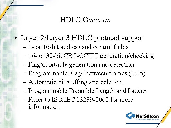
HDLC Overview • Layer 2/Layer 3 HDLC protocol support – 8 - or 16 -bit address and control fields – 16 - or 32 -bit CRC-CCITT generation/checking – Flag/abort/idle generation and detection – Programmable Flags between frames (1 -15) – Automatic bit stuffing and deletion – Programmable Preamble Length and Pattern – Refer to ISO/IEC 13239 -2002 for more information

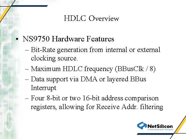
HDLC Overview • NS 9750 Hardware Features – Bit-Rate generation from internal or external clocking source. – Maximum HDLC frequency (BBus. Clk / 8) – Data support via DMA or layered BBus Interrupt – Four 8 -bit or two 16 -bit address comparison registers, allowing for Receive Addr. filtering

HDLC Overview • NS 9750 Hardware Features, continued – Transmit Handshake via CTS (Clear To Send) signal – Counter for Discarded Frames due to CRC Errors or non-matching frame address fields – Error detection: • • Misaligned (non-octet) Frames Frame Length Exceeds Max Buffer Size Receive CRC Errors FIFO underrun/overrun

HDLC Configuration • Initialize per-channel Bit Rate Register to – Enable EBIT – Set TMODE = 1 and TCDR=RCDR=0 for synchronous (x 1) operation – Enable RXSRC for receive clock via GPIOs – Enable TXEXT to drive transmit clock via GPIOs – Set Clk. Mux to select BCLK as the source – Set RXCINV, TXCINV =1 to compensate for output buffer delays – Set desired N-value (refer to Hardware Ref. Manual)

HDLC Configuration • Initialize Control Register A for – Channel Enable, 8 -bit Words, Rx and Tx Interrupt or DMA Enables • Initialize Control Register B for – HDLC Mode, Address Matching, Preamble Length and Preamble Pattern • Initialize Control Register C for – # of Flag/Marks, CRC generation/checking • Initialize BBus Utility GPIO Config registers to enable desired HDLC interface pins

Hints & Kinks • Can back-to-back HDLC frames share a single idle/mark flag? – No, there must be at least one unique idle/mark flag at the start and finish of each HDLC receive frame.