Notes for ADFing ProjectLV FPGA Kory Olney USF

- Slides: 32

Notes for ADFing Project-LV FPGA Kory Olney USF Mechanical Engineering 2018

FPGA Tips ● ● A tip on multiplication and division on FPGA: It takes a long time to do proper divisions on FPGA, so if pipelining and delays are not acceptable you must avoid this! Bear in mind that multiplication and division by powers of 2 (i. e. a = b*2^n) is fast when working with integer types due to the magic of binary! Multiplying an integer by 2, 4, 8 etc or 1/2, 1/4, 1/8 is very quick. There are loads of similar tricks with binary. For this reason I try to stay in integer space on the FPGA rather than using FXP. Looking at the code you have sent, the way you handle reading information from the DMA was a little confusing to me. To keep the channels consistent, you have to make sure that the DMA is being read in multiplies of the number of channels all the time, then decimate the output array. I was thinking about it still and I have got the idea to change the size of the DMA buffer on the side of my. RIO. I extended the buffer from 1023 elements to 2047 and it is working well and I can change the sampling rate without problems. In the configure pop-up of the "Open FPGA VI Reference", uncheck the "Run the FPGA VI".

FPGA Tips Secondly, you can use timed loops to get more deterministic behaviour on your host machine. By putting your FIFO read into a timed loop, you can have more regular reads. You can increase the priority of these loops to ensure they run quickly. Jitter may always be a problem though and you should be ready to handle the buffer full case if data loss matters to you. Thirdly, a big advantage of DMA FIFO is being able to read an arbitrary number of elements at once. I usually do a 0 element FIFO. Read, which gives me the # elements remaining immediately followed by another FIFO. Read for the remaining # elements. This allows you to use the broadness of the host to take large chunks out of the FIFO in single steps. By using a combination of these approaches you should be able to avoid buffer overflow and data loss.

FPGA Considerations High throughput vs standard specs FPGA Module Overview** https: //zone. ni. com/reference/en-XX/help/371599 L-01/TOC 19. htm Optimize FPGA Usage

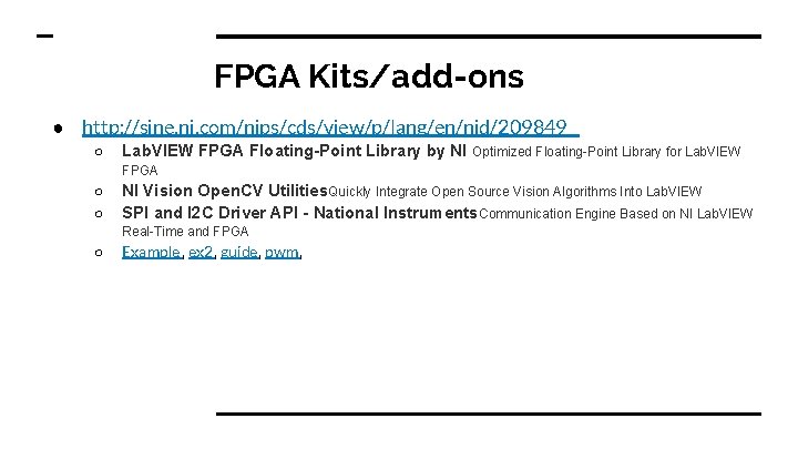
FPGA Kits/add-ons ● http: //sine. ni. com/nips/cds/view/p/lang/en/nid/209849 ○ Lab. VIEW FPGA Floating-Point Library by NI Optimized Floating-Point Library for Lab. VIEW FPGA ○ ○ NI Vision Open. CV Utilities. Quickly Integrate Open Source Vision Algorithms Into Lab. VIEW SPI and I 2 C Driver API - National Instruments. Communication Engine Based on NI Lab. VIEW Real-Time and FPGA ○ Example , ex 2, guide, pwm,

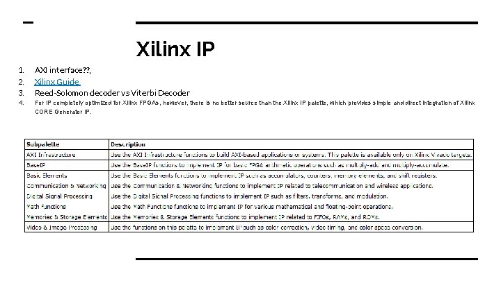
Xilinx IP 1. 2. 3. AXI interface? ? , Xilinx Guide Reed-Solomon decoder vs Viterbi Decoder 4. For IP completely optimized for Xilinx FPGAs, however, there is no better source than the Xilinx IP palette, which provides simple and direct integration of Xilinx CORE Generator IP.

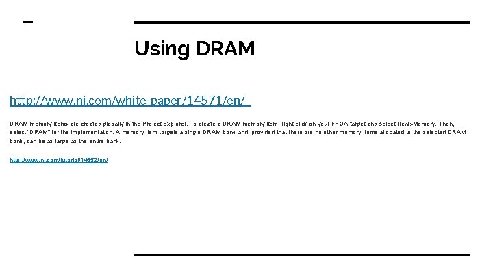
Using DRAM http: //www. ni. com/white-paper/14571/en/ DRAM memory items are created globally in the Project Explorer. To create a DRAM memory item, right-click on your FPGA target and select New» Memory. Then, select “DRAM” for the implementation. A memory item targets a single DRAM bank and, provided that there are no other memory items allocated to the selected DRAM bank, can be as large as the entire bank. http: //www. ni. com/tutorial/14652/en/

My. RIO Docs https: //en. wikipedia. org/wiki/My. RIO https: //forums. ni. com/t 5/Academic-Hardware-Products-NI/Myrio-real-time-memory/td-p/3660966 ftp: //ftp. ni. com/pub/branches/uk/educatortour/hands_on_teaching_solutions_embedded. pdf https: //forums. ni. com/t 5/Academic-Hardware-Products-NI/my. Rio-write-and-acquire-data-double-FIFO/m-p/3716013 https: //forums. ni. com/t 5/Academic-Hardware-Products-NI/my. RIO-memory-data-transfer-and-clock-rate/td-p/2789754 Manual FPGA High Performance guide

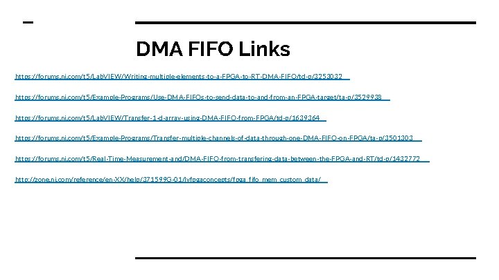
DMA FIFO Links https: //forums. ni. com/t 5/Lab. VIEW/Writing-multiple-elements-to-a-FPGA-to-RT-DMA-FIFO/td-p/3253032 https: //forums. ni. com/t 5/Example-Programs/Use-DMA-FIFOs-to-send-data-to-and-from-an-FPGA-target/ta-p/3529938 https: //forums. ni. com/t 5/Lab. VIEW/Transfer-1 -d-array-using-DMA-FIFO-from-FPGA/td-p/1639364 https: //forums. ni. com/t 5/Example-Programs/Transfer-multiple-channels-of-data-through-one-DMA-FIFO-on-FPGA/ta-p/3501303 https: //forums. ni. com/t 5/Real-Time-Measurement-and/DMA-FIFO-from-transfering-data-between-the-FPGA-and-RT/td-p/1432772 http: //zone. ni. com/reference/en-XX/help/371599 G-01/lvfpgaconcepts/fpga_fifo_mem_custom_data/

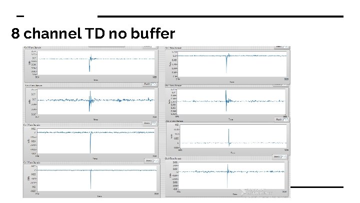
8 channel TD no buffer

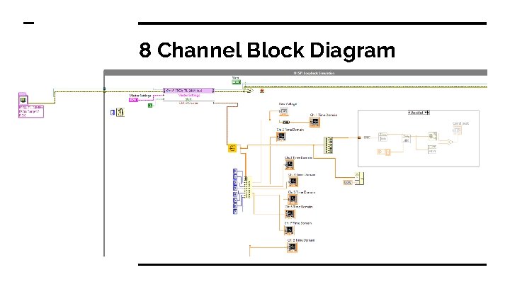
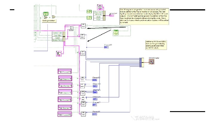
8 Channel Block Diagram

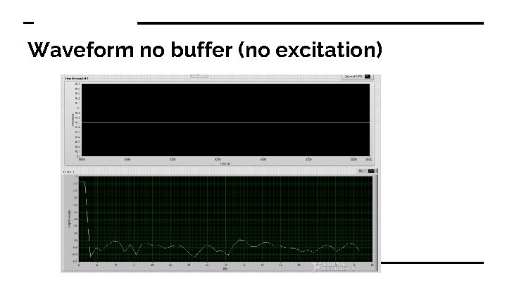
Waveform no buffer (no excitation)

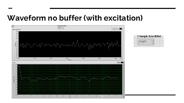
Waveform no buffer (with excitation)

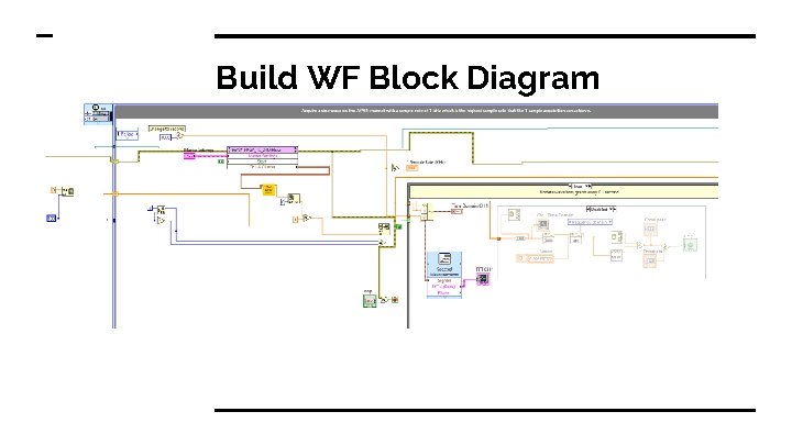
Build WF Block Diagram

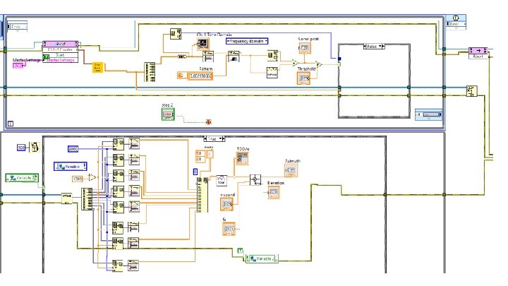
Modified IME Process

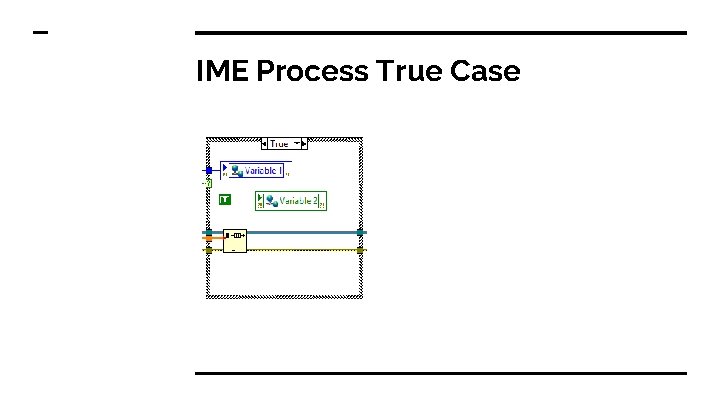
IME Process True Case

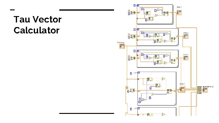
Tau Vector Calculator

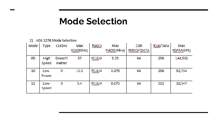
Mode Selection

ADC notes 1) Format: TDM Fixed: 001 Discrete: 010 2) Misc: Leading Clock Phase, Clock Polarity – Low, Most Significant bit First Output in 24 bit two’s complement

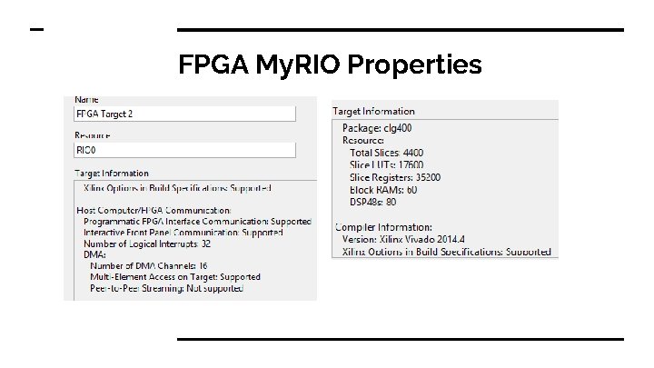
FPGA My. RIO Properties


Writing audio to wav MYRIO Youtube - NI Arduino Project Minor Help LV Makerhub Very helpful

Misc Links Sound Isolation ARDrone with LV High. Through Xilinx FIR Filter

LV Kalman Filter Links 1 NI Disc. Kalman Lava. Gcode NI Cont. Kalman Print Paper Research NI White Paper NI Demo Same?

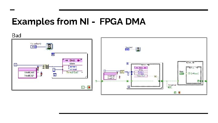
Examples from NI - FPGA DMA Bad Good

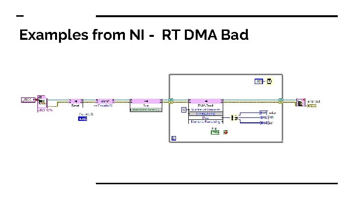
Examples from NI - RT DMA Bad

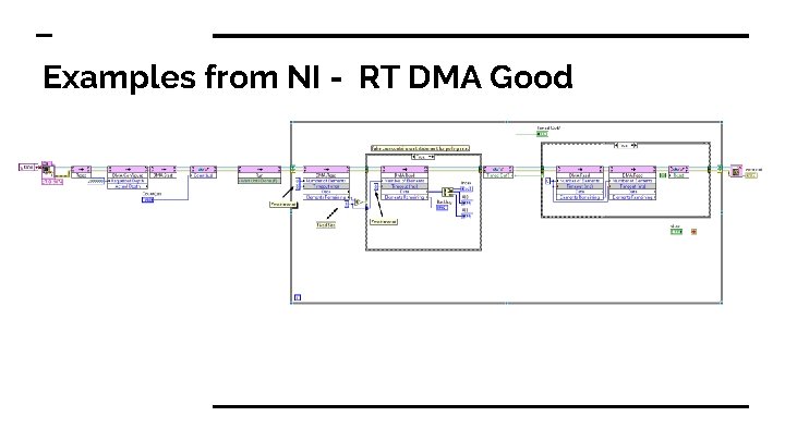
Examples from NI - RT DMA Good

Using Desktop Execution for FPGA http: //www. ni. com/white-paper/51859/en/ http: //www. ni. com/tutorial/51862/en/

More FPGA You should also consider doing the PID inside of the FPGA. PIDs work the best in a deterministic environment, and you can't get any more deterministic than on an FPGA. SCTL: https: //knowledge. ni. com/Knowledge. Article. Details? id=k. A 00 Z 000000 P 8 s. WSAS Can I use pipelining to allow more logic to execute inside the SCTL? Yes. You can use shift registers or feedback nodes to allow logic to execute in parallel and pass data between subsequent iterations of the SCTL; thus, the entire logic chain executes over multiple SCTL iterations. As with any parallel implementation in an FPGA VI, this uses additional FPGA resources. Also make sure that your timeout for writing to the FIFO is set to 0. Because the code MUST execute in a single cycle, it cannot wait.

To Do: ● ● ● ● Clean Up FPGA data types Clean up DMA FIFO Figure out how to do Desktop execution of FPGA Setup proper Configure for start of myrio, FPGA, and DMA Need to use High Throughput Install FPGA Floating Point Library Look at waveform examples (Align Waveform Timestamps)

FXP vs FLP While FPGAs can implement floating point numerical operations in general-purpose logic slices, this consumes significant resources and limits the amount and complexity of the realizable signal processing. Instead, it is common to use fixed-point representations which allow fractional data, but do not require the additional resources of a floating point representation. Deciding Using FXP on FPGA