Nonlinear Neural Networks LAB CHAPTER 16 SEQUENTIAL CIRCUIT
Nonlinear & Neural Networks LAB. CHAPTER 16 SEQUENTIAL CIRCUIT DESIGN 16. 1 16. 2 16. 3 16. 4 16. 5 16. 6 16. 7 16. 8 Summary of Design Procedure for Sequential Circuits Design Example--Code Converter Design of Iterative Circuits Design of Sequential Circuits Using ROMs and PLAs Sequential Circuit Design Using CPLDs Sequential Circuit Design Using FPGAs Simulation and Testing of Sequential Circuits Overview of Computer-Aided Design
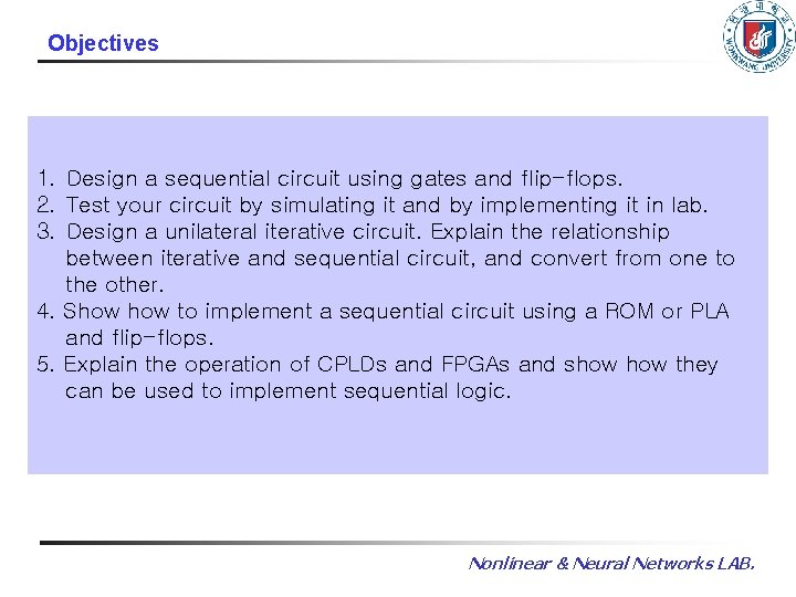
Objectives 1. Design a sequential circuit using gates and flip-flops. 2. Test your circuit by simulating it and by implementing it in lab. 3. Design a unilateral iterative circuit. Explain the relationship between iterative and sequential circuit, and convert from one to the other. 4. Show to implement a sequential circuit using a ROM or PLA and flip-flops. 5. Explain the operation of CPLDs and FPGAs and show they can be used to implement sequential logic. Nonlinear & Neural Networks LAB.
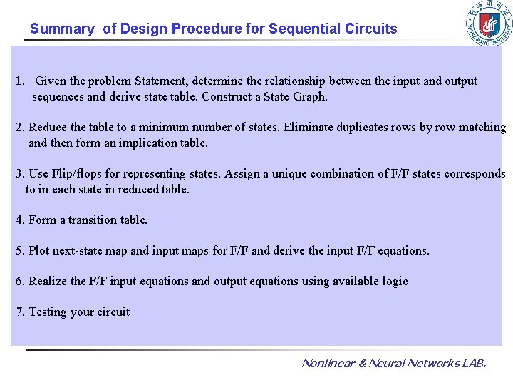
Summary of Design Procedure for Sequential Circuits 1. Given the problem Statement, determine the relationship between the input and output sequences and derive state table. Construct a State Graph. 2. Reduce the table to a minimum number of states. Eliminate duplicates rows by row matching and then form an implication table. 3. Use Flip/flops for representing states. Assign a unique combination of F/F states corresponds to in each state in reduced table. 4. Form a transition table. 5. Plot next-state map and input maps for F/F and derive the input F/F equations. 6. Realize the F/F input equations and output equations using available logic 7. Testing your circuit Nonlinear & Neural Networks LAB.
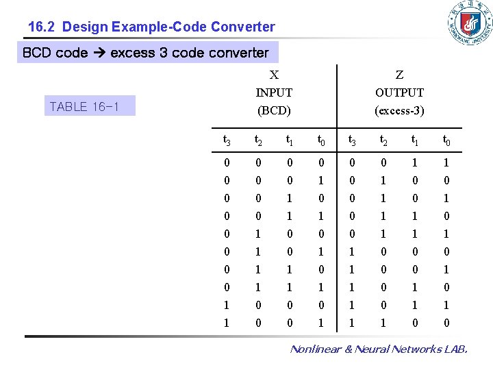
16. 2 Design Example-Code Converter BCD code excess 3 code converter X INPUT (BCD) TABLE 16 -1 Z OUTPUT (excess-3) t 3 t 2 t 1 t 0 0 0 0 0 1 1 0 0 1 1 0 0 0 1 0 1 0 1 0 0 0 1 1 1 0 0 1 1 0 1 0 1 0 Nonlinear & Neural Networks LAB.
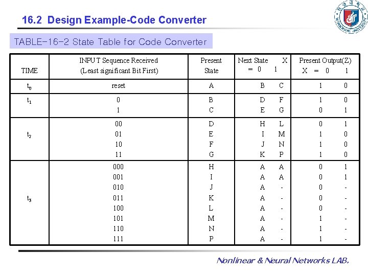
16. 2 Design Example-Code Converter TABLE-16 -2 State Table for Code Converter TIME INPUT Sequence Received (Least significant Bit First) Present State Next State X = 0 1 t 0 reset A B C 1 0 t 1 0 1 B C D E F G 1 0 0 1 00 01 10 11 D E F G H I J K L M N P 0 1 1 0 000 001 010 011 100 101 110 111 H I J K L M N P A A A A A - 0 0 0 1 1 1 - t 2 t 3 Present Output(Z) X = 0 1 Nonlinear & Neural Networks LAB.
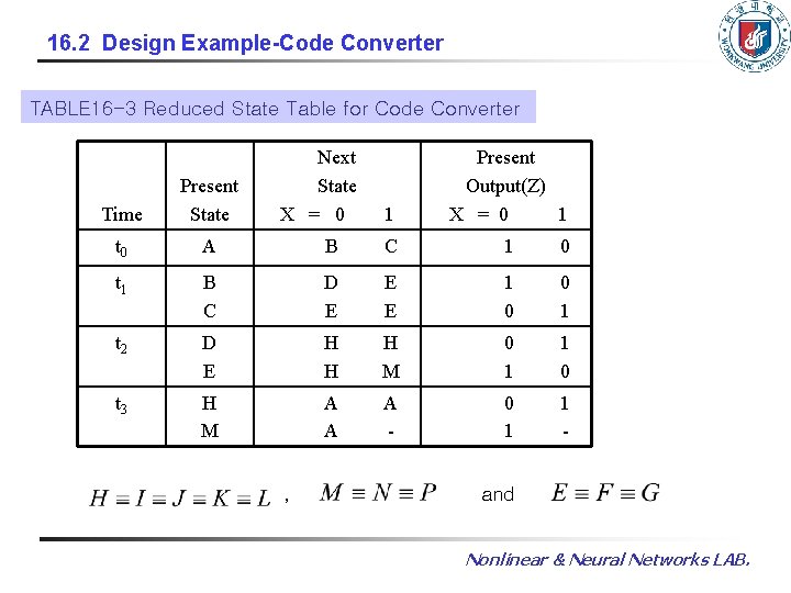
16. 2 Design Example-Code Converter TABLE 16 -3 Reduced State Table for Code Converter 1 Present Output(Z) X = 0 1 B C 1 0 B C D E E E 1 0 0 1 t 2 D E H H H M 0 1 1 0 t 3 H M A A A - 0 1 1 - Time Present State t 0 A t 1 Next State X = 0 , and Nonlinear & Neural Networks LAB.
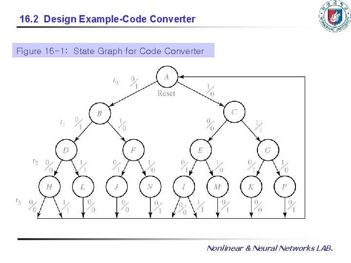
16. 2 Design Example-Code Converter Figure 16 -1: State Graph for Code Converter Nonlinear & Neural Networks LAB.
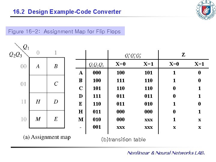
16. 2 Design Example-Code Converter Figure 16 -2: Assignment Map for Flip Flops Z A B C D E H M - 000 101 110 011 010 001 X=0 X=1 100 111 110 011 000 xxx 101 110 011 010 000 xxx 1 1 0 0 1 x 0 0 1 1 0 1 x x (b)transition table Nonlinear & Neural Networks LAB.
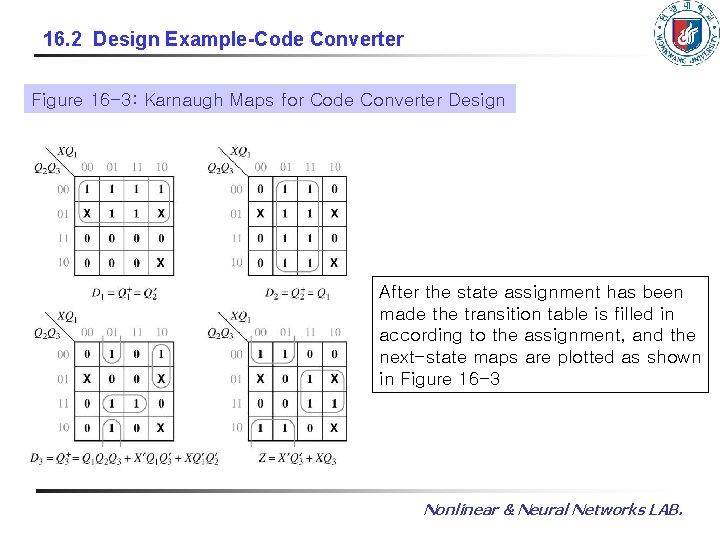
16. 2 Design Example-Code Converter Figure 16 -3: Karnaugh Maps for Code Converter Design After the state assignment has been made the transition table is filled in according to the assignment, and the next-state maps are plotted as shown in Figure 16 -3 Nonlinear & Neural Networks LAB.
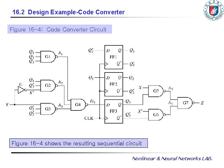
16. 2 Design Example-Code Converter Figure 16 -4: Code Converter Circuit Figure 16 -4 shows the resulting sequential circuit Nonlinear & Neural Networks LAB.
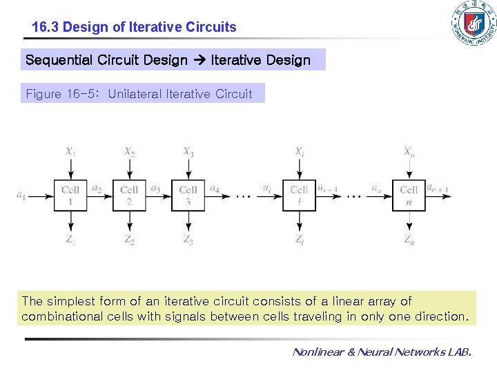
16. 3 Design of Iterative Circuits Sequential Circuit Design Iterative Design Figure 16 -5: Unilateral Iterative Circuit The simplest form of an iterative circuit consists of a linear array of combinational cells with signals between cells traveling in only one direction. Nonlinear & Neural Networks LAB.
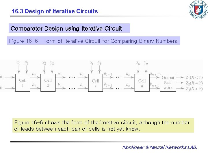
16. 3 Design of Iterative Circuits Comparator Design using Iterative Circuit Figure 16 -6: Form of Iterative Circuit for Comparing Binary Numbers Figure 16 -6 shows the form of the iterative circuit, although the number of leads between each pair of cells is not yet know. Nonlinear & Neural Networks LAB.
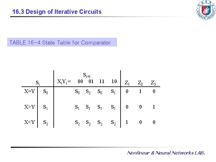
16. 3 Design of Iterative Circuits TABLE 16 -4 State Table for Comparator Xi. Yi = Si Si+1 00 01 11 10 Z 1 Z 2 Z 3 X=Y S 0 S 2 S 0 S 1 0 X>Y S 1 S 1 S 1 0 0 1 X<Y S 2 S 2 S 2 1 0 0 Nonlinear & Neural Networks LAB.
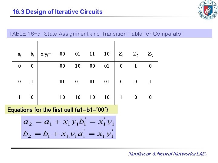
16. 3 Design of Iterative Circuits TABLE 16 -5 State Assignment and Transition Table for Comparator ai bi 0 xiyi= 00 01 11 10 Z 1 Z 2 Z 3 0 00 10 00 01 0 0 1 01 01 0 0 1 1 0 10 10 1 0 0 Equations for the first cell (a 1=b 1=’ 00’) Nonlinear & Neural Networks LAB.
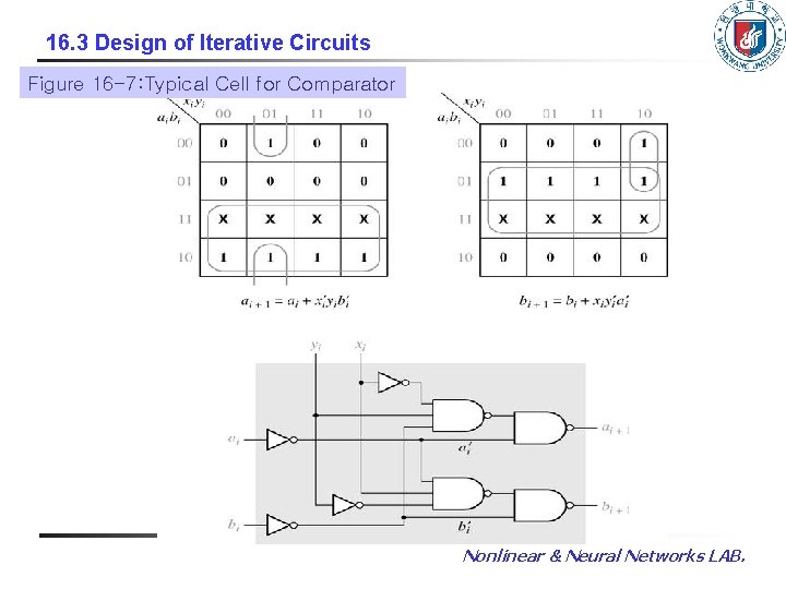
16. 3 Design of Iterative Circuits Figure 16 -7: Typical Cell for Comparator Nonlinear & Neural Networks LAB.
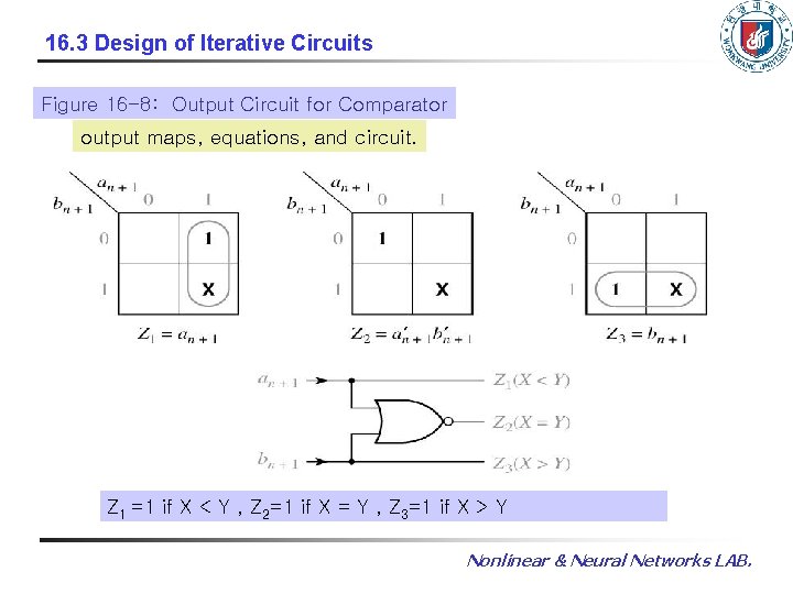
16. 3 Design of Iterative Circuits Figure 16 -8: Output Circuit for Comparator output maps, equations, and circuit. Z 1 =1 if X < Y , Z 2=1 if X = Y , Z 3=1 if X > Y Nonlinear & Neural Networks LAB.
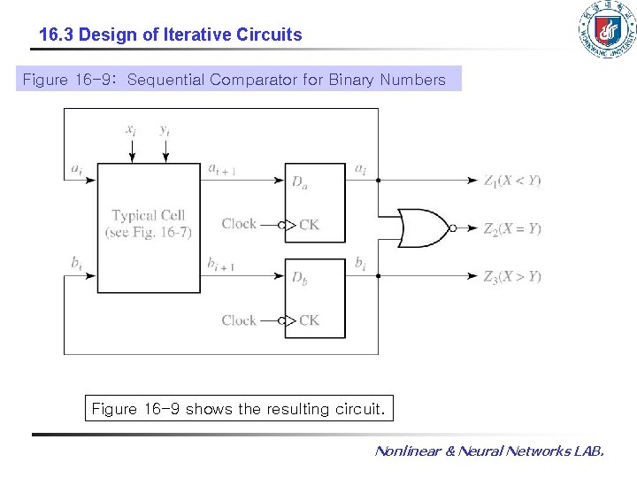
16. 3 Design of Iterative Circuits Figure 16 -9: Sequential Comparator for Binary Numbers Figure 16 -9 shows the resulting circuit. Nonlinear & Neural Networks LAB.

16. 4 Design of Sequential Circuits Using ROMs and PLAs Sequential Circuit can be designed using a ROM and F/F’s TABLE 16 -6: Revisit the Code Converter Design (a)State table Present State Next State X= Present Output (Z) 0 1 A B B C X= 0 1 C 1 0 D E E E 1 0 0 1 D E H H H M 0 1 1 0 H M A A A - 0 1 1 - Nonlinear & Neural Networks LAB.
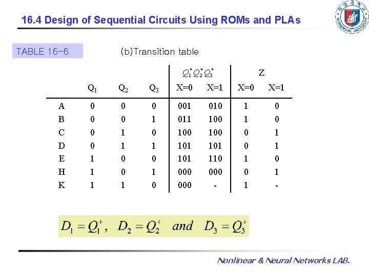
16. 4 Design of Sequential Circuits Using ROMs and PLAs TABLE 16 -6 (b)Transition table + + + Q 1 Q 2 Q 3 A B C D E H K Z Q 1 Q 2 Q 3 X=0 X=1 0 0 1 1 1 0 0 1 0 1 0 001 011 100 101 000 010 100 101 110 000 - 1 1 0 0 1 1 0 1 - Nonlinear & Neural Networks LAB.
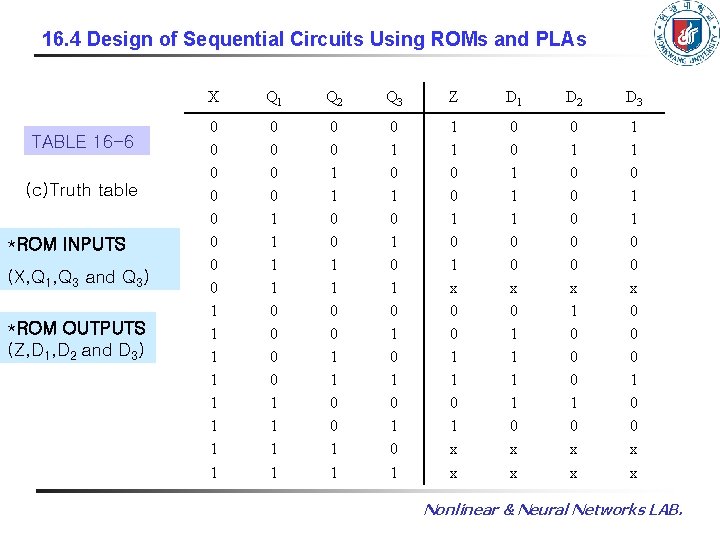
16. 4 Design of Sequential Circuits Using ROMs and PLAs TABLE 16 -6 (c)Truth table *ROM INPUTS (X, Q 1, Q 3 and Q 3) *ROM OUTPUTS (Z, D 1, D 2 and D 3) X Q 1 Q 2 Q 3 Z D 1 D 2 D 3 0 0 0 0 1 1 1 1 0 0 1 1 0 1 0 1 1 1 0 0 1 x 0 0 1 1 0 1 x x 0 0 1 1 1 0 0 x 0 1 1 0 x x 0 1 0 0 0 x 1 0 0 0 1 0 x x 1 1 0 0 x 0 0 0 1 0 0 x x Nonlinear & Neural Networks LAB.
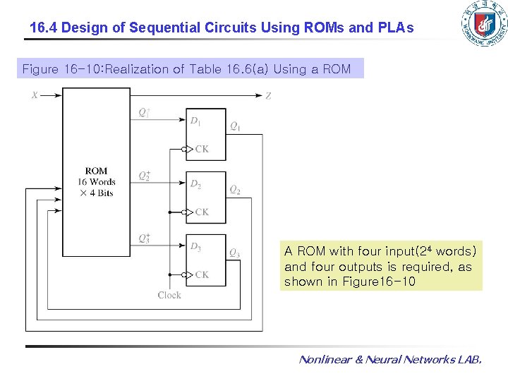
16. 4 Design of Sequential Circuits Using ROMs and PLAs Figure 16 -10: Realization of Table 16. 6(a) Using a ROM A ROM with four input(24 words) and four outputs is required, as shown in Figure 16 -10 Nonlinear & Neural Networks LAB.
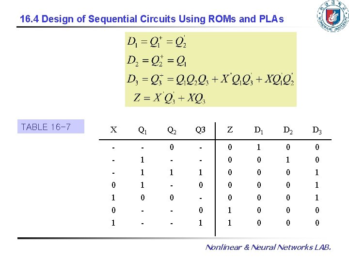
16. 4 Design of Sequential Circuits Using ROMs and PLAs TABLE 16 -7 X Q 1 Q 2 Q 3 Z D 1 D 2 D 3 0 1 1 1 1 0 - 0 1 0 - 1 0 0 0 0 0 1 1 1 0 0 Nonlinear & Neural Networks LAB.
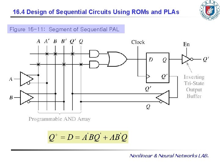
16. 4 Design of Sequential Circuits Using ROMs and PLAs Figure 16 -11: Segment of Sequential PAL Nonlinear & Neural Networks LAB.
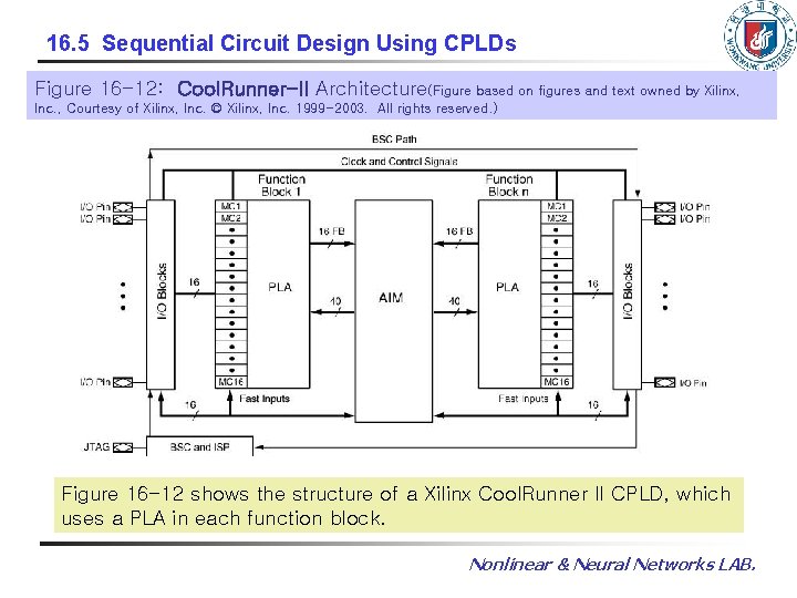
16. 5 Sequential Circuit Design Using CPLDs Figure 16 -12: Cool. Runner-II Architecture(Figure based on figures and text owned by Xilinx, Inc. , Courtesy of Xilinx, Inc. © Xilinx, Inc. 1999 -2003. All rights reserved. ) Figure 16 -12 shows the structure of a Xilinx Cool. Runner II CPLD, which uses a PLA in each function block. Nonlinear & Neural Networks LAB.
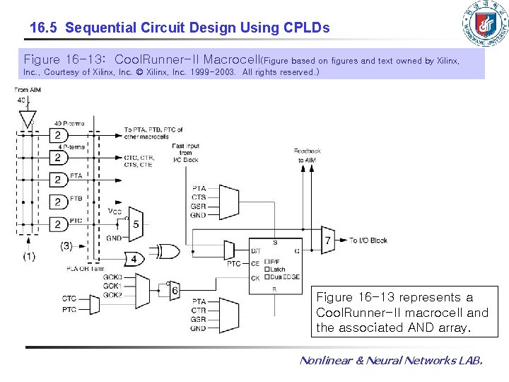
16. 5 Sequential Circuit Design Using CPLDs Figure 16 -13: Cool. Runner-II Macrocell(Figure based on figures and text owned by Xilinx, Inc. , Courtesy of Xilinx, Inc. © Xilinx, Inc. 1999 -2003. All rights reserved. ) Figure 16 -13 represents a Cool. Runner-II macrocell and the associated AND array. Nonlinear & Neural Networks LAB.
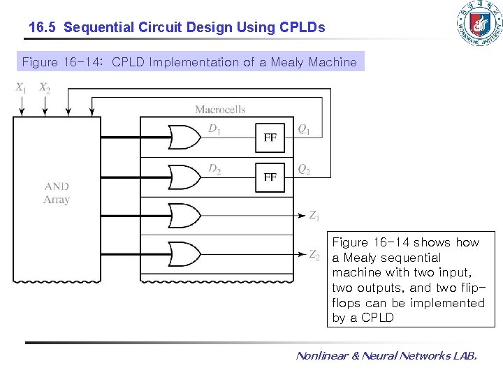
16. 5 Sequential Circuit Design Using CPLDs Figure 16 -14: CPLD Implementation of a Mealy Machine Figure 16 -14 shows how a Mealy sequential machine with two input, two outputs, and two flipflops can be implemented by a CPLD Nonlinear & Neural Networks LAB.
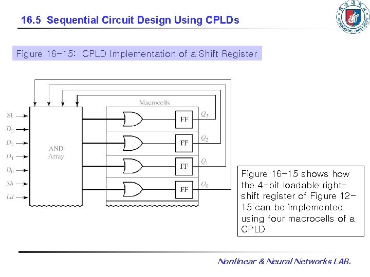
16. 5 Sequential Circuit Design Using CPLDs Figure 16 -15: CPLD Implementation of a Shift Register Figure 16 -15 shows how the 4 -bit loadable rightshift register of Figure 1215 can be implemented using four macrocells of a CPLD Nonlinear & Neural Networks LAB.
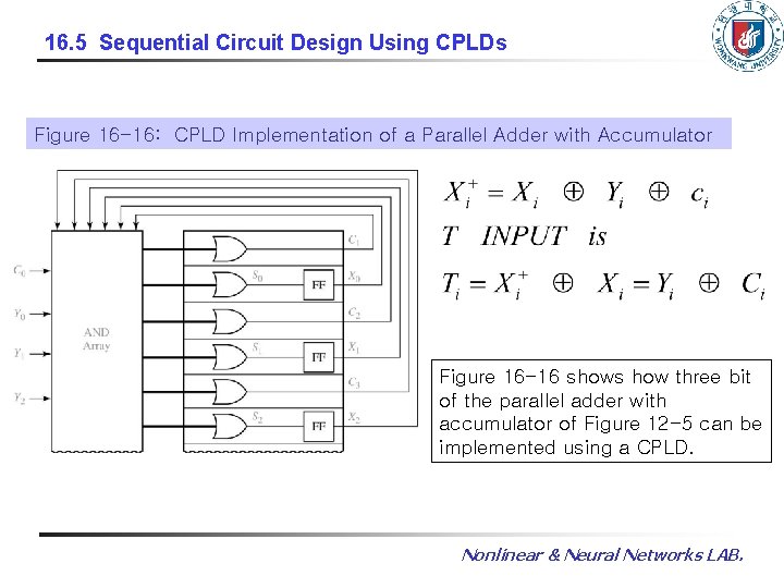
16. 5 Sequential Circuit Design Using CPLDs Figure 16 -16: CPLD Implementation of a Parallel Adder with Accumulator Figure 16 -16 shows how three bit of the parallel adder with accumulator of Figure 12 -5 can be implemented using a CPLD. Nonlinear & Neural Networks LAB.
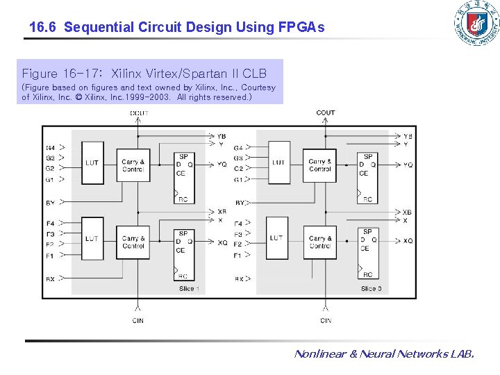
16. 6 Sequential Circuit Design Using FPGAs Figure 16 -17: Xilinx Virtex/Spartan II CLB (Figure based on figures and text owned by Xilinx, Inc. , Courtesy of Xilinx, Inc. © Xilinx, Inc. 1999 -2003. All rights reserved. ) Nonlinear & Neural Networks LAB.
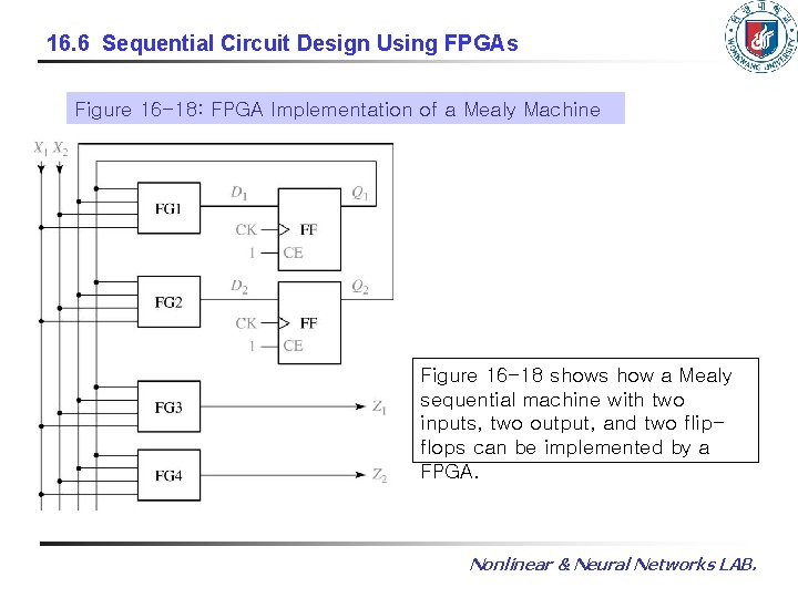
16. 6 Sequential Circuit Design Using FPGAs Figure 16 -18: FPGA Implementation of a Mealy Machine Figure 16 -18 shows how a Mealy sequential machine with two inputs, two output, and two flipflops can be implemented by a FPGA. Nonlinear & Neural Networks LAB.
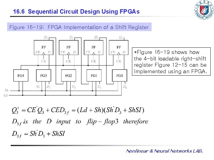
16. 6 Sequential Circuit Design Using FPGAs Figure 16 -19: FPGA Implementation of a Shift Register *Figure 16 -19 shows how the 4 -bit loadable right-shift register Figure 12 -15 can be implemented using an FPGA. Nonlinear & Neural Networks LAB.
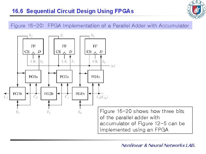
16. 6 Sequential Circuit Design Using FPGAs Figure 16 -20: FPGA Implementation of a Parallel Adder with Accumulator Figure 16 -20 shows how three bits of the parallel adder with accumulator of Figure 12 -5 can be implemented using an FPGA Nonlinear & Neural Networks LAB.
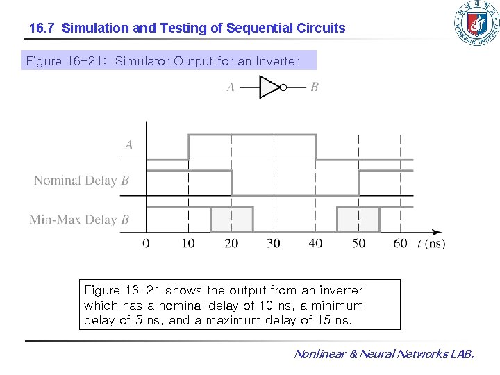
16. 7 Simulation and Testing of Sequential Circuits Figure 16 -21: Simulator Output for an Inverter Figure 16 -21 shows the output from an inverter which has a nominal delay of 10 ns, a minimum delay of 5 ns, and a maximum delay of 15 ns. Nonlinear & Neural Networks LAB.
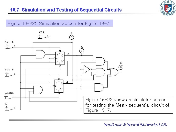
16. 7 Simulation and Testing of Sequential Circuits Figure 16 -22: Simulation Screen for Figure 13 -7 Figure 16 -22 shows a simulator screen for testing the Mealy sequential circuit of Figure 13 -7. Nonlinear & Neural Networks LAB.
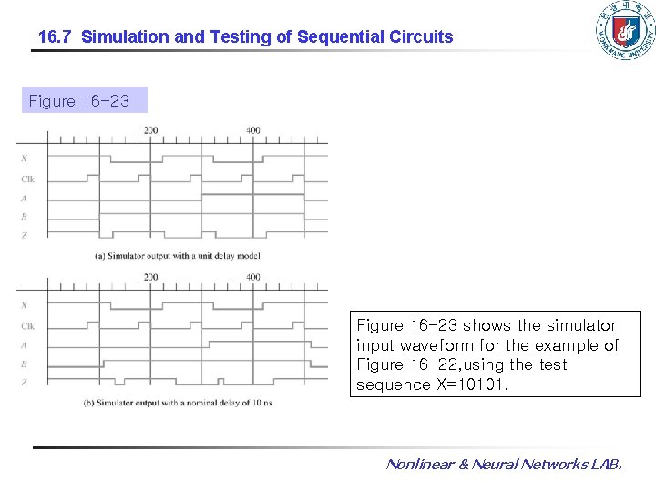
16. 7 Simulation and Testing of Sequential Circuits Figure 16 -23 shows the simulator input waveform for the example of Figure 16 -22, using the test sequence X=10101. Nonlinear & Neural Networks LAB.
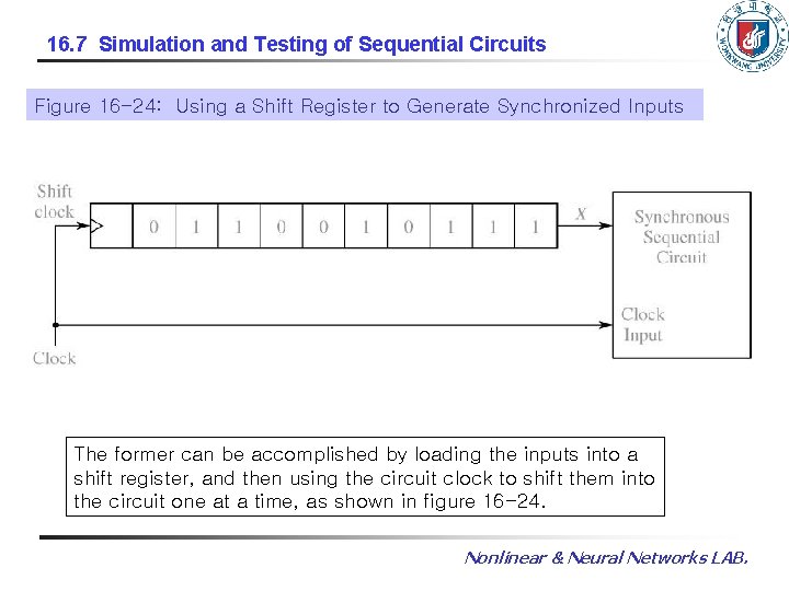
16. 7 Simulation and Testing of Sequential Circuits Figure 16 -24: Using a Shift Register to Generate Synchronized Inputs The former can be accomplished by loading the inputs into a shift register, and then using the circuit clock to shift them into the circuit one at a time, as shown in figure 16 -24. Nonlinear & Neural Networks LAB.
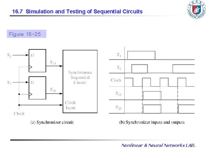
16. 7 Simulation and Testing of Sequential Circuits Figure 16 -25 Nonlinear & Neural Networks LAB.
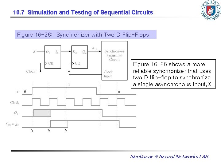
16. 7 Simulation and Testing of Sequential Circuits Figure 16 -26: Synchronizer with Two D Flip-Flops Figure 16 -26 shows a more reliable synchronizer that uses two D flip-flop to synchronize a single asynchronous input, X Nonlinear & Neural Networks LAB.
16. 7 Overview of Computer-Aided Design Functions performance of CAD tools • Generation and Minimization of logic equation • Generation of bit patterns for programming PLD’s • Schematic Capture • Simulation • Synthesis tools • IC design and Layout • Test Generation • PC board Layout Nonlinear & Neural Networks LAB.
16. 7 Simulation and Testing of Sequential Circuits Design a small digital systems with an FPGA 1. Draw a block diagram of the digital system. Define the required control signals and construct state graph and describes the required sequence of operations 2. Workout a detailed logic design using gates, F/F, register, counter, adders, etc… (HDL) 3. Construct a logic diagram using a schematic capture program(HDL) 4. Simulate and debug the logic diagram and make any necessary corrections to the design(HDL) 5. Run an implementation program that fits the design into the target FPGA 6. Simulation and verifying 7. Download the bit pattern into FPGA and test. Nonlinear & Neural Networks LAB.
- Slides: 40