Noise Immunity Transients and ESD Practical Design Considerations

- Slides: 15

Noise Immunity Transients and ESD Practical Design Considerations prepared by Prof. George Slack (EE) Copyright © 2006 Rochester Institute of Technology All rights reserved. EDGE™

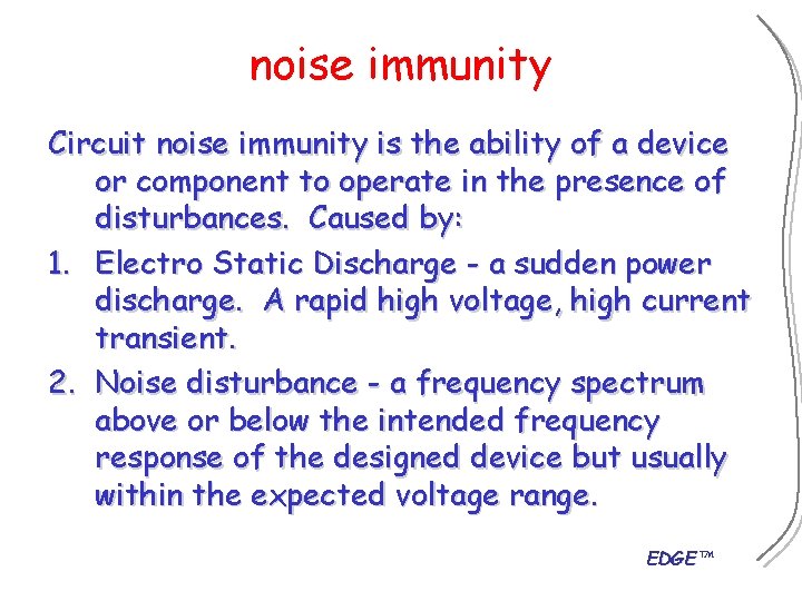
noise immunity Circuit noise immunity is the ability of a device or component to operate in the presence of disturbances. Caused by: 1. Electro Static Discharge - a sudden power discharge. A rapid high voltage, high current transient. 2. Noise disturbance - a frequency spectrum above or below the intended frequency response of the designed device but usually within the expected voltage range. EDGE™

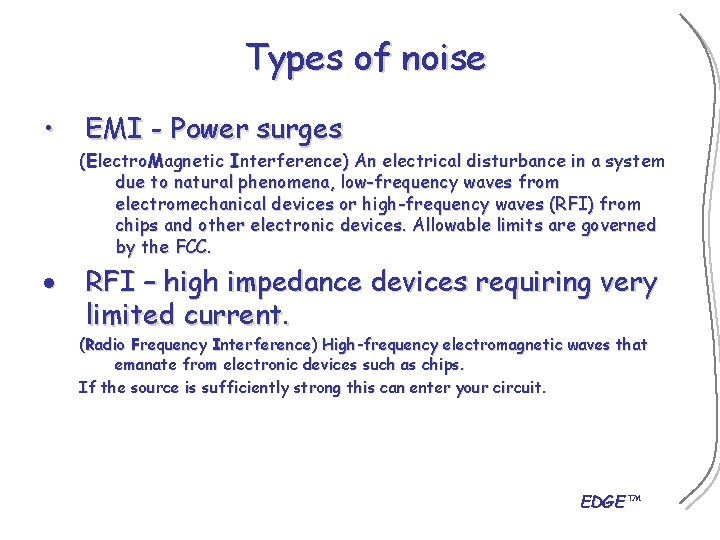
Types of noise • EMI - Power surges (Electro. Magnetic Interference) An electrical disturbance in a system due to natural phenomena, low-frequency waves from electromechanical devices or high-frequency waves (RFI) from chips and other electronic devices. Allowable limits are governed by the FCC. RFI – high impedance devices requiring very limited current. (Radio Frequency Interference) High-frequency electromagnetic waves that emanate from electronic devices such as chips. If the source is sufficiently strong this can enter your circuit. EDGE™

When is Noise Immunity design needed? • Senior Design I – Paper Design wks 1 -8 • Senior Design II – Prototype device testing wks 1 - 3. – Pre-integration testing with lab equipment DUT (device under test). Wks 3 - 6 EDGE™

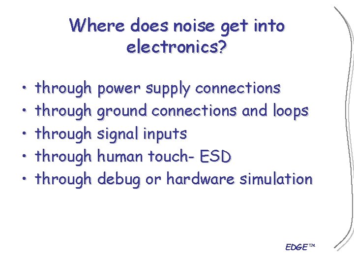
Where does noise get into electronics? • • • through power supply connections through ground connections and loops through signal inputs through human touch- ESD through debug or hardware simulation EDGE™

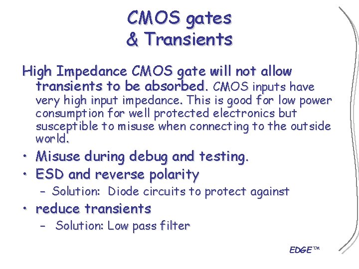
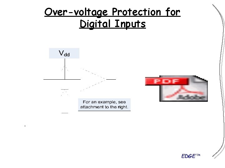
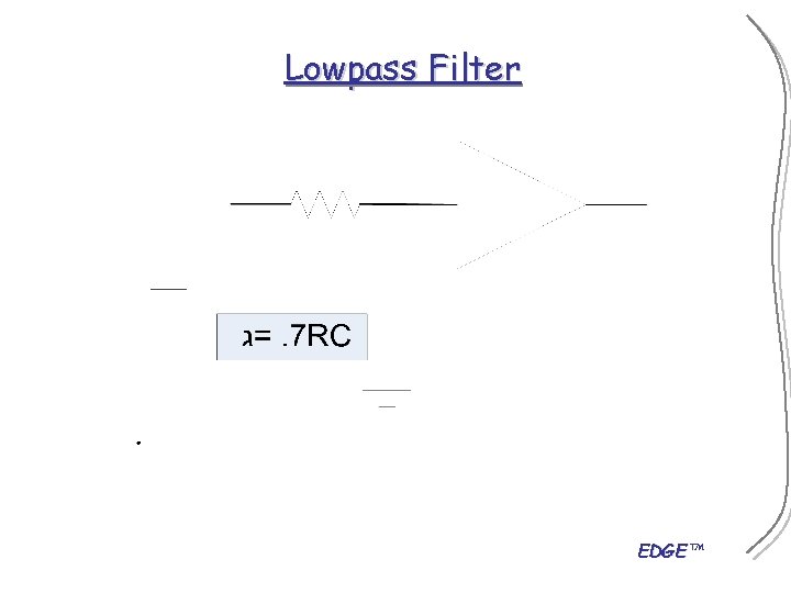
CMOS gates & Transients High Impedance CMOS gate will not allow transients to be absorbed. CMOS inputs have very high input impedance. This is good for low power consumption for well protected electronics but susceptible to misuse when connecting to the outside world. • Misuse during debug and testing. • ESD and reverse polarity – Solution: Diode circuits to protect against • reduce transients – Solution: Low pass filter EDGE™

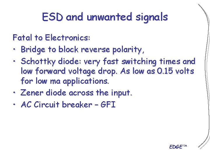
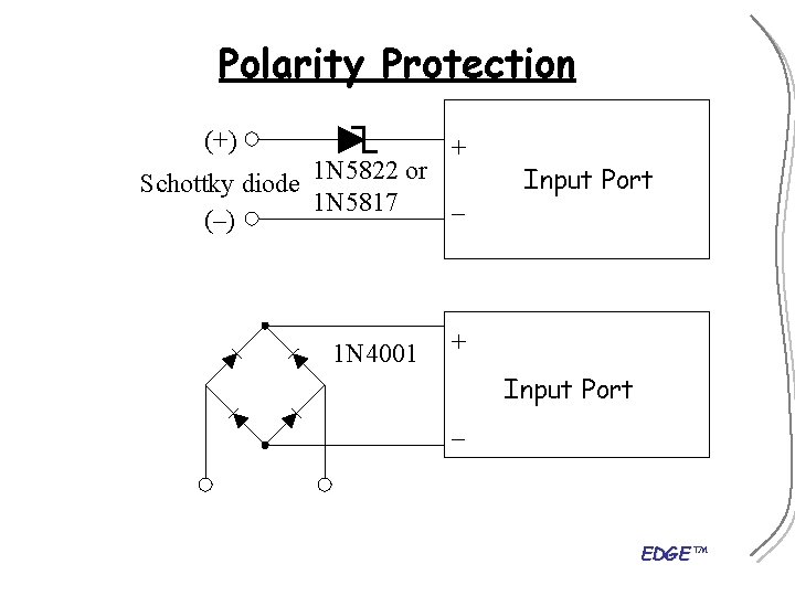
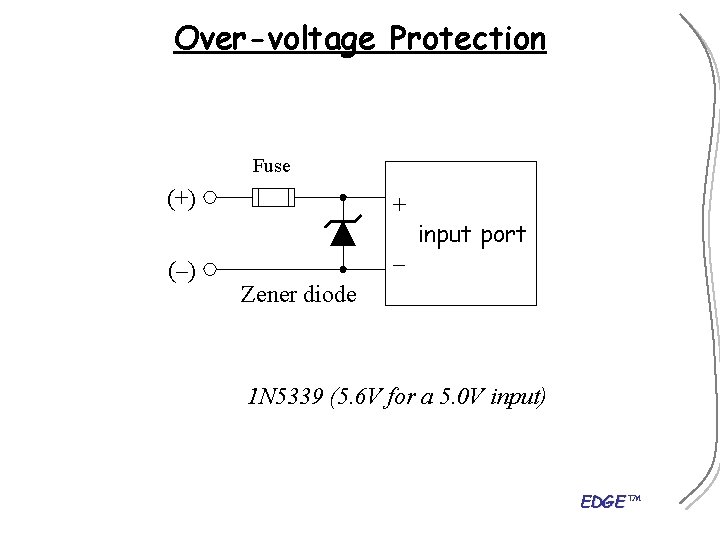
ESD and unwanted signals Fatal to Electronics: • Bridge to block reverse polarity, • Schottky diode: very fast switching times and low forward voltage drop. As low as 0. 15 volts for low ma applications. • Zener diode across the input. • AC Circuit breaker – GFI EDGE™

Polarity Protection (+) + Schottky diode 1 N 5822 or 1 N 5817 – (–) 1 N 4001 Input Port + Input Port – EDGE™

Over-voltage Protection Fuse (+) (–) + input port – Zener diode 1 N 5339 (5. 6 V for a 5. 0 V input) EDGE™

Over-voltage Protection for Digital Inputs EDGE™

Lowpass Filter EDGE™

Knowing Your Design Specifications 1. CRITICAL: When considering various input and output devices, acquire manufacture’s specification sheets. (Also, many spec sheets show application circuits which may speed up your design. ) 2. Noise versus signal response needs (i. e. CMOS versus TTL ). 3. Control Voltage (Vdd vary from 1. 5 VDC to 12 VDC typically) 4. Needed minimum Signal Transient Response. 5. RLC loads (dangerous current and voltage spikes) 6. Apply to Thevenin Equivalent Circuits – Source electronics – Device being driven EDGE™

Isolating Noise • Digital and Analog Optocoupler /Optoisolators – an electronic device that uses optics to transfer a signal while keeping the receiving and transmitting circuits electrically isolated • http: //www. optoinc. com/optocouplers 1. html • Digital Isolators – Power Islation • Somewhat expensive ($1/ channel) but good isolation. • http: //www. analog. com (Analog Devices) • nsec repsonse, > 30 VDC outputs, • Power connections - Design for Transit current spikes. • Shielding at high frequency response needs • Fiber Optics at giga hz response needs What does not work? – Fuses are typically ineffective since a fuse is too slow to stop ESD and violent transient current but good for harness short-circuit or misuse. EDGE™

Isolators • Analog Devices, Isolators http: //www. analog. com/en/sub. Cat/0, 2879, 767%255 F 827%255 F 0%255 F, 00. html • Isolators: http: //www. analog. com/en/prod/0, 2877, ADu. M 2401, 00. html EDGE™

Articles, recommendations, components and spec sheets short circuit protection circuits; http: //www. electronicstalk. com/guides/short-circuit-protection. html Manufacture’s short circuit IC. http: //www. maxim-ic. com/appnotes. cfm/appnote_number/38 EMI/ RRI Filters http: //www. onsemi. com/Power. Solutions/taxonomy. do? id=298 EMI RFI EDN Article http: //www. edn. com/article/CA 326921. html Conductors http: //www. bussmann. com/library/techspec/Tech. Spec 19_sup. pdf#search=%22 short %20 circuit%20 protection%22 Design Standards UL 489 and UL 1077 standards http: //www. elecdesign. com/Articles/Index. cfm? AD=1&Article. ID=5195 EDGE™