New Results in Reversible Logic Marek Perkowski LDL

New Results in Reversible Logic. Marek Perkowski LDL seminar, January 18, 2002

Plan • 1. recent results in Reversible Logic obtained by our group. • 2. review the work of De. Vos, Storme and others. • 3. new reversible gates in CMOS. • 4. reversible fuzzy logic. • 5. methods to create reversible gates of higher number of inputs/outputs. • 6. new regular structures and synthesis methods for them. • 7. an approach to synthesize arbitrary multi-output functions with no garbage. • 8. the system of EDA tools for reversible/quantum logic. • 9. binary, data mining, multiple-valued and quantum benchmarks

Think about a gate as an input/output constraint A B X Y A 0 0 B 0 1 1 1 0 reversible A=X A XOR B=Y R(input, output) = R(<A, B>, <X, Y>) = Permute(2, 3) constraint <<1, 0> , <1, 1>> YES <0, 0> ==> <0, 0> <1, 0> <== <1, 1> <<1, 1> , <0, 1>> NO

Reversible computation. • Charles Bennett, IBM, 1973. – Logical reversibility of computation, • IBM J. Res. Dev. 17, 525 (1973). This principle applies also to combinational circuits that we build, but is this a best way, question for us to answer

Landauer's principle • Landauer's principle: logic computations that are not reversible, necessarily generate heat: – i. e. k. Tlog(2), for every bit of information that is lost. where k is Boltzmann's constant and T the temperature. • For T equal room temperature, this package of heat is small, i. e. 2. 9 x 10 -21 joule, but non-negligible. • In order to produce zero heat, a computer is only allowed to perform reversible computations. • Such a logically reversible computation can be `undone': the value of the output suffices to recover what the value of the input `has been'. • The hardware of a reversible computer cannot be constructed from the conventional gates • On the contrary, it consists exclusively of logically reversible building blocks.

• Tomasso Toffoli, 1980: There exists a reversible gate which could play a role of a universal gate for reversible circuits. Q(3) : (x, y, z)==>(x, y, z@xy) @ denotes EXOR x y z z@xy A B reversible Fredkin and Toffoli created the first (3, 3) universal gate A A XOR B Toffoli Gate

Quantum XOR • Of special interest is the controlled-NOT or reversible XOR gate: XOR : (x; y) ==> (x, x @ y); by @ we denote EXOR (modulo-2 sum) x x y x@y These notations were introduced by physicists and they are inconsistent with standard electrical engineering notations, however it will be convenient for us to use both notations.

Swapping bits using XOR cascade With the circuit Constructed from three Quantum XORs, we can swap two bits: (x, y) ==> (x, x@y) ==> (y, x) Conclusion: in quantum logic you pay for crossing wires!!! cascade Of importance in quantum, quantum dot, but not CMOS
 The first step is to")
Use of Toffoli Gate • From three-bit Toffoli-Gate Q(3) The first step is to show that from the three-bit Toffoli Gate Q (3) we can construct an nbit Toffoli Gate Q (n). The n-bit gate works as follows: (x 1, x 2, …, x n-1, xn)==>(x 1, x 2, …, x n-1 y@x 1 x 2…x n-1 ) The construction requires one extra bit of scratch space. For example, we construct Q (4) circuit from Q (3) circuits as follows: Q 4 from three Q 3 Scratch space
 gate is")
Use of Toffoli Gate • The purpose of the last Q (3) gate is to reset the scratch bit back to its original value 0. • With one more gate we can obtain an implementation of Q (4) that works irrespective of the initial value of the scratch bit: We can eliminate the last gate if we don’t mind flipping value of the scratch bit
 , any")
Use of Toffoli Gate • When we need to construct Q (k) , any available extra bit will do, since the circuit returns the scratch bit to its original value. • The next step is to note that, by conjugating Q(n) with NOT gates, we can in effect modify the value of the control string that “triggers" the gate. • For example, the circuit flips the value of y if x 1 x 2 x 3 = 010, and it acts trivially otherwise.

Use of Toffoli Gate • Flips the value of y if x 1 x 2 x 3 = 010, and it acts trivially otherwise. • Thus this circuit transposes the two strings 0100 and 0101. • In like fashion, with Q(n) and NOT gates, we can devise a circuit that transposes any two n-bit strings that differ in only one bit. • (The location of the bit where they differ is chosen to be the target of the Q (n) gate. )

Q 0 A B 1 R 0 1 P Q P A C A circuit from two multiplexers R 0 1 B Its schematics This is a reversible gate, one of many Notation for Fredkin Gates C

Q 0 A B 1 C R 0 P 1 A 0 C Margolus Gate A 1 B

Toffoli Gate • The 3 * 3 Toffoli gate is described by these equations: P P = A, Q = B, R = AB C, • Toffoli gate is an example of two-through gates, because two of its inputs are given to the output. Q R + * A B C
 B A C")
P Q P R + + * A Q Feynman (b) B A C B Toffoli P + 0 R + 1 * * A Q B C Kerntopf Gate

Kerntopf Gate • The Kerntopf gate is described by equations: P = 1 @ A @ B @ C @ AB, Q = 1 @ AB @ C @ BC, R = 1 @ A @ B @ AC. • When C=1 then P = A + B, Q = A * B, R = !B, so AND/OR gate is realized on outputs P and Q with C as the controlling input value. • When C = 0 then P = !A * ! B, Q = A + !B, R = A @ B. • 18 different cofactors!

Kerntopf Gate • As we see, the 3*3 Kerntopf gate is not a onethrough nor a two-through gate. • Despite theoretical advantages of Kerntopf gate over classical Fredkin and Toffoli gates, so far there are no published results on optical or CMOS realizations of this gate.

How to build garbage-less circuits A Toffoli B C D Fredki n Feynm an copy Feynm an Feyn man Fred kin Feyn man copy F 2 from spy D To ffo li A B C inputs reconstructed F 1 from spy 2 outputs no garbage A, B, C, D are original inputs This process is informationally reversible It can be in addition thermodynamically reversible width = 4 delay = 9

Observations • We reduced garbage at the cost of delay and number of gates • We were not able to reduce the width of the scratchpad register

01 10 1 Variable 11 01 0 X 3 xor 3 Shannon Conservative circuit = the same number of ones in inputs and outputs Davio Majority X 2 xor 2 Examples of balanced functions = half of Kmap are ones

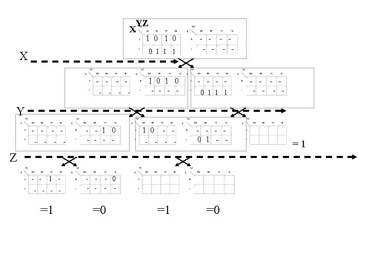
YZ X 0 1 YZ X 1 - 0 - 1 - X 00 01 11 10 1 0 0 1 1 1 - - - - - YZ X 0 - YZ g f garbage 0 X garbage Y 0 h fg 0 garbage hfg 1 1 1 Z garbage 1 0 1 1 garbage 0 1 fgh 1 - garbage i gf -

Lattice Structure for Multiple-valued and Binary Logic • Realizes every binary symmetric function • Realizes every nonsymmetric function by repeating variables • Realizes piece-wise linear multivalued functions Patented by Pierzchala and Perkowski 1994/1999
 A")
Lattice Structure for Binary Logic F = S 1, 3 (A, B, C) A 0 1 B C 0 S 0 1 1 0 S 1 S 2 S 3

YZ X 0 1 YZ X 1 - 0 - 1 - X 00 01 11 10 1 0 0 1 1 1 - - - - - YZ X 0 - YZ g f garbage 0 X garbage Y 0 h fg 0 garbage hfg 1 1 1 Z garbage 1 0 1 1 garbage 0 1 fgh 1 - garbage i gf -

Control gates as building blocks for reversible computers • A. De Vos 1 , B. Desoete 2 , F. Janiak 3 , and A. Nogawski 3 – 1 Universiteit Gent and Imec v. z. w. , B-9000 Gent, Belgium 2 Universiteit Gent, B-9000 Gent, Belgium 3 Politechnika L odzka, PL 90 -924 L odz, Poland

• As an illustration, two reversible 4 -bit carrylook-ahead adders in 0. 8 m c-MOS have been built.

2 Simple control gates • 2. 1 Definition • A gate with k inputs (A 1, A 2 , …, Ak) and k outputs (P 1, P 2, , . . . , …, Pk), satisfying Pi = Ai for all i { 1, 2, . . , k } Pk = f(A 1, A 2, …, Ak-1) Ak with f an arbitrary boolean function of k boolean arguments, is called a simple control gate. • The number k is called the width of the gate. • The logic inputs A 1, A 2, . . . , Ak-1 are named the controlling bits, whereas the input Ak is the controlled bit. • Finally, the function f is called the control function.

2. 2 Properties • Any simple control gate is reversible. • We cascade two identical simple control gates, yielding Pk = [ f(A 1, A 2, …, A k-1) f(A 1, A 2, …, Ak-1) ] Ak and thus Pi = Ai for all i, because of the two boolean identities X X = 0 and 0 Y = Y. • The result is thus the k-bit follower. • In other words: any simple control gate is its own inverse, and thus is necessarily reversible.

• Cascading two arbitrary simple control gates (one with control function f’ and one with control function f’’) results in a new simple control gate, with control function f’ f’’. • Therefore the simple control gates of width k together with the operation cascading form a group. • The group has elements.

• and thus can be built into a square geometry, provided we use dual line electronics, i. e. any signal X is accompanied by its counterpart NOT X. • Fig. 1 shows Pk is connected to Ak if f = 0 but is connected to A’k (short notation for NOT Ak) if f = 1.
")
• Because a boolean function f(A 1, A 2, …. , A k-1) can always be written – either as an `OR of ANDs' (often referred to as `sum of minterms') – or as an `AND of ORs' (often referred to as `product of maxterms'), we can implement Pk = f(A 1, A 2, …. , A k-1) A k in the square, using – either four parallel connections of series connections of switches – or four series connections of parallel connections of switches – or a combination of both.

• Each switch is composed of one n-MOS transistor in parallel with one p-MOS transistor (forming together a transmission gate). • This leads to a reversible electronic implementation in dual-line passtransistor logic: so-called r-MOS technology [9]. • Such logic is naturally suited for adiabatic addressing [10] [11] [12]. • All energy supplied to the outputs Pk and P’k comes from the inputs Ak and A’k, i. e. not from separate power lines. • • 9. A. De Vos: Reversible computing. Progress in Quantum Electronics 23 (1999) 1 -49 10. B. Desoete and A. De Vos: Optimal charging of capacitors. In: A. Trullemans and J. Spars½ (eds. ): Proc. 8 th Int. Workshop Patmos, Lyngby (Oct. 1998) 335 -344 11. A. De Vos and B. Desoete: Equipartition principles in finite-time thermodynamics. Journal of Non-Equilibrium Thermodynamics 25 (2000) 1 -13 12. A. De Vos, B. Desoete, A. Adamski, P. Pietrzak, M. Sibi nski, and T. Widerski: Design of reversible logic circuits by means of control gates. In: D. Soudris, P. Pirsch, and E. Barke (eds. ): Proc. 10 th Int. Workshop Patmos, G. ottingen (Sept. 2000) 255 -264

Fig. 1. Implementation of the function f A , k with the help of four switches f Ak

Example of extending functions to reversible functions
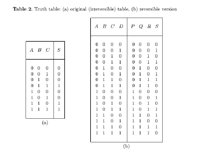

Fig. 2. Implementation of boolean Table 2 using 12 switches

Fig. 2. Implementation of boolean Table 2 using 28 switches • An alternative approach makes use of standard cells, where the particular function f(A, B, C), to be XORed with D, is hardwired by the vias between the Metal 1 and Metal 2 layers of the chip. • These vias are displayed as small black squares in Fig. 2 b. • The programmable gate however needs 2 k+1 - 4 = 28 switches.

Fig. 3. Decomposition of a control gate into simple control gates • Because each output 3. Control is only one boolean function f away from gates the inputs, its logic depth is only 1. • We call such gates control gates, as each output Pi is either equal to the controlled bit Ai or to its inverse A’i, 3. 1 Definition depending on the When we cascade k simple control gates (one of width k, value of its k-1 one of width k-1, . . . , and one of width 1), in the way of Fig. 3, we have a new gate of width k. controlling inputs A 1, A 2, . . , Ai-1.

• We thus come to the definition of a control gate: – a logic gate with k inputs (A 1, A 2, …. , A k) and k outputs (P 1, P 2, …. , P k), satisfying Pi = fi (A 1, A 2, …. , A k) Ai for all i {1, 2, …, k} with fi arbitrary boolean functions of (i-1) arguments, is called a control gate. • Note that a control gate with width k has (k-1) controlling bits (A 1, A 2, …. , A k) as well as (k-1) controlled bits (A 2, …. , A k) • We remark that the above definition is somewhat more general than the preliminary definition presented at Patmos 2000 [12].

3. 2 Properties • As any control gate is composed of simple control gates and any simple control gate is reversible, the control gate is thus also reversible. • The inverse of a simple control gate is equal to itself. • This is not the case with an arbitrary control gate. • The inverse of the control gate of Fig. 3 consists of first putting the simple control gate f 1, then the simple control gate f 2, etc. • Now the cascading of two simple control gates of different width is not commutative. • Thus an arbitrary control gate and its reverse are not necessarily equal, the simple building blocks appearing in opposite order.

• Two control gates (one with control functions f’ and one with control functions f’’), when cascaded, form a new control gate, – with control functions fi (A 1, A 2, …. , A i-1) =f 0 – Ai fi(A 1; A 2; : : : ; Ai-1) = f 0 i – (A 1, A 2, …. , A i-1) f’’ – (A 1; A 2; : : : ; Ai -1) XOR f 00 i ( f 0 1 (: ) XOR A 1; f 0 2 (A 1) XOR A 2; : : : ; f 0 -1 (A 1; A 2; : : : ; Ai-2) XOR Ai 1 ) :

• Thus, the control gates of width k, together with the cascading operation, form a group. • This group has 2^(2 k-1) elements and is solvable, but not abelian.

4 Carry-look-ahead adder • To demonstrate the flexibility of using control gates, we present here, as an example, a 4 -bit carry-look-ahead adder, as an alternative to the classical, i. e. ripple adder. • An n-bit ripple adder consists of 2 n gates of type CONTROLLED NOT and 2 n gates of the CONTROLLED NOT type [12]. • Its logic depth increases with increasing n. • In order to make the calculation less deep, and thus faster, we replace the ripple adder by a carry-look-ahead adder. • For the carry-look-ahead (or c. l. a. ) [13], we first need to implement the calculation of the n generator bits Gi and the n propagator bits Pi from the n addend bits Ai and the n augend bits Bi: – Gi = Ai AND Bi – Pi = Ai XOR Bi:

4 Carry-look-ahead adder • Next we need to calculate the n carry-out bits Ci from the single carryin bit C 0, the n generator bits, and the n propagator bits. In its simplest form, the 4 -bit carry-look-ahead adder implements the following equations: – – C 1 = G 0 OR (C AND C 0) C 2 = G 1 OR (P 1 AND (G 0 OR (P 0 AND C 0))) C 3 = G 2 OR (P 2 AND (G 1 OR (P 1 AND (G 0 OR (P 0 AND C 0))))) C 4 = G 3 OR (P 2 AND (G 2 OR (P 2 AND (G 1 OR (P 1 AND (G 0 OR (P 0 AND C 0))))))) : • This can be performed by a control gate with 2 n + 1 bits controlling n other bits (i. e. k = 3 n + 1). • The electronic implementation of this gate consists of n squares, counting 8 n(n + 2) transistors. • In the third and final step, the adder calculates the n sum bits: – Si = Pi XOR Ci :
, of Ci+1, and")
5 Results • Putting the three parts (calculation of (Gi; Pi), of Ci+1, and of Si) together, we see that the logic depth d of the resulting n-bit c. l. a. adder is 3, independent of n. • Note that we consider the NOT as a gate of zero depth. • Indeed, in dual line hardware, the NOT gate is merely an interchange of the two lines and thus costs neither silicon area, nor time delay, nor power dissipation. • Fig. 4 shows the 4 -bit c. l. a. adder. • For sake of clarity, the 8 preset input lines and the 12 garbage output lines are not shown, nor are the inverters (i. e. the NOT gates). • Each logic gate has an equal number of logic inputs and logic outputs, a number we call the width w of the gate. • The full circuit has depth d = 3, width w = 17, and transistor count t = 320. For an arbitrary n, we have d = 3, w = 4 n + 1 and t = 8 n(n + 6). • For comparison: the ripple adder has d = n + 1, w = 3 n + 1 and t = 48 n. • Thus for any number n > 2, the c. l. a. adder is less deep (and thus faster) than its ripple counterpart. • At the other side, for any number n, the c. l. a. circuit is more complex than the ripple circuit, the hardware overhead becoming quite substantial for large n.

• Fig. 5 shows the 4 -bit implementation in the 0. 8 m c-MOS n-well technology CYE of Austria Mikro Systeme. • The n-MOS transistors have length L equal to 0. 8 m and width W equal to 2 m. • The p-MOS transistors have L = 0. 8 m and W = 6 m. • The threshold voltages are 0. 85 volt (n-MOS) and 0. 75 volt (p-MOS). • -Vss ranging from 1 volt to 3 volts. • The whole chip (bonding pads included) measures 1. 9 mm 1. 2 mm. • The chip has been tested successfully, with power supply voltage Vdd -Vss ranging from 1 volt to 3 volts.

• A c. l. a. chip, applying hardware-programmed control gates, is designed. • It contains as many as t = 64/3 (4 n + 3 n - 1) = 5696 transistors and measures 2. 5 mm * 2. 0 mm. • In the recent literature, other 4 -bit c. l. a. adders [14] [15], and even an 8 -bit [16] c. l. a. adder with adiabatic/reversible gates have been presented. • Our design should not at all be considered as just one more such a circuit. • Our c. l. a. adders should be regarded as specific examples of the design philosophy we have developed: reversible control gate logic.

Fig. 4. Schematic diagram of reversible carry-look-ahead four-bit adder

Fig. 5. Microscope photograph of c. MOS reversible carry-look-ahead fourbit adder

• Fig. 6 a shows the experimental transient output C 4 for augend B = 1101 and addend A changing quasi-adiabatically from 0010 to 0011 with charging time = 50 s. • Fig. 6 b shows the power dissipation estimated by Spectre simulations (including parasitics) for Vdd = - Vss = 2 V, as a function of .

References • 1. R. Landauer: Irreversibility and heat generation in the computing process. I. B. M. Journal of Research and Development 5 (1961) 183 -191 • 2. C. Bennett and R. Landauer: The fundamental physical limits of computation. Sc. American 253 (July 1985) 38 -46 • 3. R. Landauer: Information is physical. Physics Today 44 (May 1991) 23 -29 • 4. T. Toffoli: Reversible computing. In: J. De Bakker and J. Van Leeuwen (eds. ): 7 th Colloquium on Automata, Languages and Programming, Springer, Berlin (1980) 632{644 • 5. E. Fredkin and T. Toffoli: Conservative logic. Int. Journal of Theoretical Physics 21 (1982) 219 -253 • 6. L. Storme, A. De Vos, and G. Jacobs: Group theoretical aspects of reversible logic gates. Journal of Universal Computer Science 5 (1999) 307 -321 • 7. R. Feynman: Quantum mechanical computers. Optics News 11 (1985) 11 -20

References • 8. R. Feynman: Feynman lectures on computation (A. Hey and R. Allen, eds. ). Addison-Wesley, Reading (1996) • 9. A. De Vos: Reversible computing. Progress in Quantum Electronics 23 (1999) 1 -49 • 10. B. Desoete and A. De Vos: Optimal charging of capacitors. In: A. Trullemans and J. Spars½ (eds. ): Proc. 8 th Int. Workshop Patmos, Lyngby (Oct. 1998) 335 -344 • 11. A. De Vos and B. Desoete: Equipartition principles in finite-time thermodynamics. Journal of Non-Equilibrium Thermodynamics 25 (2000) 1 -13 • 12. A. De Vos, B. Desoete, A. Adamski, P. Pietrzak, M. Sibi nski, and T. Widerski: Design of reversible logic circuits by means of control gates. In: D. Soudris, P. Pirsch, and E. Barke (eds. ): Proc. 10 th Int. Workshop Patmos, G. ottingen (Sept. 2000) 255 -264
")
References • 13. H. Taub: Digital circuits and microprocessors. Mc Graw Hill, Auckland (1982) • 14. S. Kim and M. Papaefthymiou: True single-phase energyrecovering logic for low-power, high-speed VLSI. In: Proc. 1998 Int. Symposium on Low Power Electronics & Design, Monterey (August 1998) 167 -172 • 15. S. Kim and M. Papaefthymiou: Pipelined DSP design with true single-phase energy-recovering logic style. In: Proc. I. E. E. E. Alessandro Volta Memorial Workshop on Low Power Design, Como (March 1999) 135 -143 • 16. S. Kim and M. Papaefthymiou: Low-energy adder design with a single-phase source-coupled adiabatic logic. In: J. Spars½ and D. Soudris (eds. ): Proc. 9 th Int. Workshop Patmos, Kos (Oct. 1999) 93102

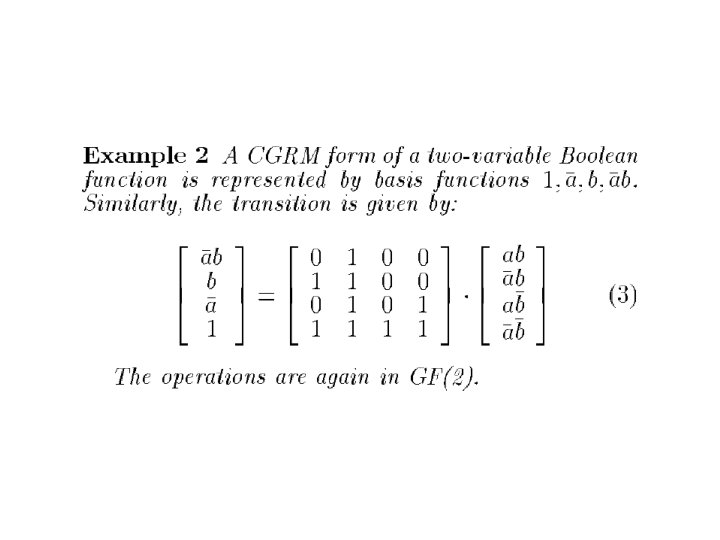
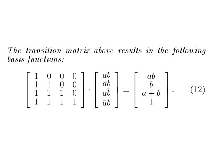
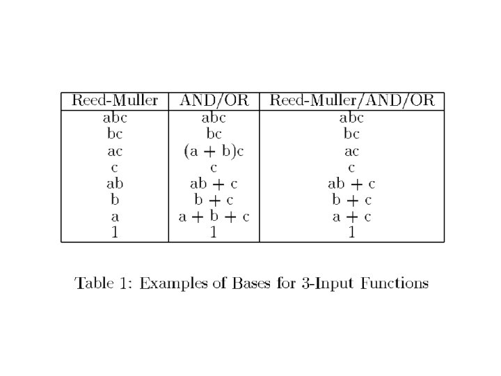
• • Example 1 In the vector space of two-variable Boolean functions, the Reed. Muller basis functions are 1, a, b, and ab, while the minterms are a b, ab, and ab. • The transition from the minterm basis to the Reed- Muller basis is given by: a b + a’b = b a b + ab’ = a

• As it can be observed, the rows of the transition matrices are linearly independent. • In general, in the space of Boolean functions, all nonsingular matrices of dimension 2 n provide the transition matrices for all possible bases. • These are the bases of Universal XOR forms (UXF).

• • • Denition 3 Let be a vector space of n-variable Boolean functions over GF(2). A Universal XOR form (UXF) is a basis in this vector space. If a basis function in a UXF can be realized as a product of literals, it is called a monoterm. In general, a term in a UXF is called a uxf-term of f.
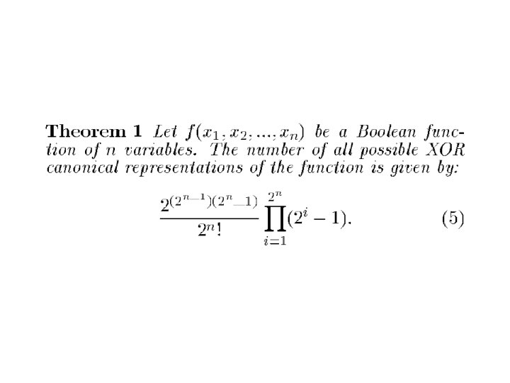

• By Theorem 1, there exist 20160/4! = 840 different XOR canonical forms for a 2 -variable function alone. • This number for a 3 -variable function is around 1. 326 * 10 14.

Figure 1: Example of a Complex Maitra Logic Array

Figure 2: An Example of a Complex Plane of a CMLA

Group Properties
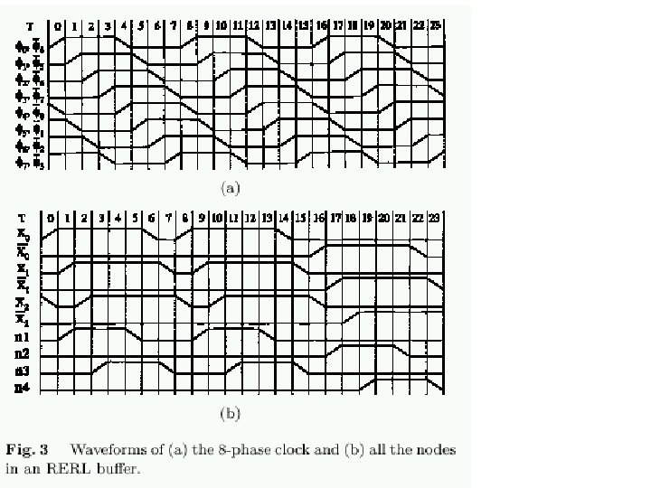
 Reversible Energy Recovery Logic")
Buffer • Corresponds to shaded parts in (c) Reversible Energy Recovery Logic
 indicates the direction and path")
Reversible Pipeline Connection • A shaded arrow in (b) indicates the direction and path of energy charging or discharging • F, G, and H are forward functions of each logic stage • F-1, G-1 and H-1 are their backward functions, respectively • A solid line in the buffer symbol of “c” indicates the energy flow • Clocks connected to the isolation switches are not shown explicitly in the symbol

Symbol for a buffer chain

Symmetry Analysis by De Vos • Logic gates with three input bits and three output bits have a privileged position within fundamental computer science. • They are a sufficient building block for constructing arbitrary reversible boolean networks and therefore are the key to reversible digital computers. • Such computers can, in principle, operate without heat production. • There exist as many as 8! = 40, 320 different 3 -bit reversible truth tables • The question: which ones to choose as building blocks. • Because these gates form a group with respect to the operation `cascading', we can apply group theoretical tools, in order to make such a choice. • We will study permutations

4 Calculation with three bits • There exist 88 = 16, 777, 216 different truth tables with 3 inputs and 3 outputs. – Among them, only 8! = 40, 320 are reversible. • However, 48 of these truth tables fall apart into three separate 1 -bit reversible tables and another 288 fall apart into one 1 -bit and one (true) 2 -bit reversible gate. • Thus, among the 40, 320 reversible 3 -bit gates, only 39, 984 are true 3 -bit gates.

4 Calculation with three bits • Two well-known examples are – the Fredkin gate – the Feynman's CONTROLLED NOT gate • The truth table of the Feynman gate is given in Table 3 c. • The. Fredkin gate is shown in Table 5 a. Feynman Gate

4 Calculation with three bits • Both have a particular property: each is a universal primitive. • This means that any boolean function of any finite number of logic input variables can be implemented by combining a finite number of such building blocks. • The proof consists of two steps: – one first proves that the building block suffices to implement the NAND function (Table 1 b), – then one refers to the fact that the NAND function is a universal primitive.

4 Calculation with three bits • The latter step is a well-known theorem. • The former step is demonstrated by introducing a so-called preset: we keep one or two inputs fixed and look how the three outputs are function of the remaining input(s). • Among the 39, 984 reversible true 3 -bit gates, many have the universality property. • It is clear, however, that the number 39, 984 is too large to allow `manual' inspection. • We have to recur to computer-algebra software specially dedicated to group theory, such as GAP and Magma – In the present study, we have chosen the GAP approach, because of GAP's builtin commands Double. Coset and Double. Cosets.
 EXCHANGER, (b)")
Table 4: The three generators of the 2 -bit reversible gates: (a) EXCHANGER, (b) NOT, (c) CONTROLLED NOT.
 Fredkin's conservative gate, (b) a `pseudoinverting' gate.")
Table 5: Truth tables: (a) Fredkin's conservative gate, (b) a `pseudoinverting' gate.

5 Groups and subgroups • Because of the universality property of some of the 3 -bit reversible gates, we now continue the w = 3 case in more detail. • When a reversible 3 -bit gate x is cascaded by a reversible 3 -bit gate y (i. e. when the P output of gate x is connected to the A input of y, etc. ), then a new reversible 3 -bit gate is formed, denoted xy. • The 40, 320 reversible truth tables of width 3 therefore form a group, say R, which is isomorphic to the symmetric group S 8.

5 Groups and subgroups • The identity element of the group is the 3 -bit follower (P = A, Q = B, and R = C). In GAP, each element of R is denoted by its permutation notation. • E. g. the follower is denoted (), whereas the CONTROLLED NOT is written (7, 8), because the seventh and the eighth line of the truth table (i. e. Table 3 c) are interchanged.

Groups E, F and G • In order to classify the large number of elements of the group R, we will introduce in the following paragraphs three different important subgroups, namely E with 6 elements, F with 48 elements, and finally G with 1, 344 elements. • They are ordered as E<F<G<R • where < denotes `is proper subgroup of'. • By means of each of these three subgroups, we will partition R into double cosets, which will serve as equivalence classes in the application of Section 6.
 EXCHANGER, (b) EXCHANGER, (c) NOT, (d) CONTROLLED NOT.")
Table 6: The subgroup generators: (a) EXCHANGER, (b) EXCHANGER, (c) NOT, (d) CONTROLLED NOT. From top to bottom, four different representations: schematic, set of logic equations, truth table, and permutation. Gates (a) and (b) together generate subgroup E; Gates (a), (b), and (c) together generate subgroup F; Gates (a), (b), (c), and (d) together generate subgroup G.

e 1 and e 2 • An important subgroup of R is formed by the follower together with the five elements representing mere relabellings. • Table 6 a shows the example e 1, satisfying P = A, Q = C, and R = B, i. e. performing an exchange of B and C. In permutation notation, gate e 1 is written (2, 3)(6, 7). • A second example is e 2 or (3, 5)(4, 6). See Table 6 b. Table 6: The subgroup generators: (a) EXCHANGER, (b) EXCHANGER, (c) NOT, (d) CONTROLLED NOT. From top to bottom, four different representations: schematic, set of logic equations, truth table, and permutation. Gates (a) and (b) together generate subgroup E; Gates (a), (b), and (c) together generate subgroup F; Gates (a), (b), (c), and (d) together generate subgroup G.

• An important subgroup of R is formed by the follower together with the five elements representing mere relabellings. • Table 6 a shows the example e 1, satisfying P = A, Q = C, and R = B, i. e. performing an exchange of B and C. In permutation notation, gate e 1 is written (2, 3)(6, 7). • A second example is e 2 or (3, 5)(4, 6). • See Table 6 b.

Subgroup E of exchangers • Together these two elements generate the whole subgroup of exchangers. • The importance of this subgroup E comes from the fact that these gates are trivial to implement in any technology. – E. g. in electronics, they consist merely of cross-overs of metal lines. • The subgroup E of exchange gates contains six elements. • It is denoted G 6 (SW) by Rayner and Newman and is isomorphic to the symmetric group S 3.

Subgroup E of Exchangers • Results from GAP show us that E partitions the full group R into 1, 172 distinct double cosets. • A double coset of an element g consists of all elements e´ ge´´ , where both e´ and e´´ are elements of the subgroup E. • This means that, although there exist 40, 320 different reversible gates, there are only 1, 172 `really different' ones, as soon as we consider exchangers as `for free'. • From these 1, 172 gates, all other 39, 148 gates can be fabricated by merely adding one relabelling gate to the left and one to the right.

Enlarging subgroup E • In a next step, we can enlarge the above subgroup E, by introducing the inverter or NOT gate. • One can either invert A (i. e. realize the gate P = NOT A, Q = B, and R = C), or invert B (i. e. realize P = A, Q = NOT B , and R = C), or invert C (P = A, Q = B, and R = NOT C ). • As an example, the cycle notation of the last gate is (1, 2)(3, 4)(5, 6)(7, 8). • These three inverters (denoted i 1, i 2 , and i 3 ) generate a subgroup of order 23= 8, isomorphic to Z 23, where Z 2 is the cyclic group of order 2.

E+I=F • Together, the subgroup E of exchangers and the subgroup I of inverters generate a new subgroup F of order 48, isomorphic to S 3: Z 23, the semi-direct product of S 3 and Z 23. • The elements of F are exactly the 48 gates mentioned in Section 4, i. e. the 3 -bit gates that fall apart into three distinct 1 -bit gates.

52 distinct double cosets • Using GAP, we find that the subgroup F partitions the full group R into 52 distinct double cosets. • This means that, although there exist 40, 320 different reversible gates, there are only 52 `really different' ones, if we consider both exchangers and inverters as `for free'. • From these 52 gates, corresponding to representatives of the 52 distinct double cosets of F, all other 40, 268 gates can be fabricated by merely adding one free gate to the left and one to the right.

The list of all double cosets • Table 7 gives a list of all 52 double cosets ki. Note that GAP gives them in a specific order, which has no a priori meaning for the user. We also get a representative ri of class ki.

Table 7: The double cosets ki of F in R.

• Again GAP's way of choosing this representative is not transparent to the user. • The different double cosets constructed with F sometimes have different size. • Table 7 gives ni , i. e. the number of elements in the double coset. • At first sight, it may be a surprise that a double coset may contain less than 482 = 2, 304 members. • This is caused by the fact that different products f´gf´´ (with g a member of R and both f´ and f´´ members of F) can lead to equal results.

• It is possible to prove that each double coset contains a number of elements which is a multiple of 48. • Double coset k 1 is the subgroup F itself, with the follower () as representative r 1. • We remark that Feynman's gate (7, 8) is the representative r 4 of class k 4. • If we take the elements of subgroup F and add the representative ri of ki

Table 7: The double cosets ki of F in R.

• If we take the elements of subgroup F and add the representative ri of ki , then these 49 elements together generate a subgroup. • Such a subgroup is called the closure of F and ri. Its order we denote by mi in Table 7. • From GAP, we learn that · Sometimes mi is as large as 40, 320, meaning that the closure of F and ri is the full group R. In other words, any element of R can then be written as a finite product of form f´ri f´´´´. . . , i. e. a finite cascade of ri gates separated by merely exchangers and/or inverters. In this case, we call ri universal. · Sometimes mi is as small as ni +48, meaning that ki together with k 1 forms a subgroup. Any product of the form f´ri f´´´ri f´´´´. . . then generates either an element of k 1 or an element of ki. The only double cosets with this property are k 3 and k 31.

lattice of all subgroups containing F and contained in R. • In order to get more insight into the 52 double cosets in which R is divided, we construct the lattice of all subgroups containing F and contained in R. • This yields a set of partially ordered subgroups: Figure 2: The lattice.

Figure 2: The lattice.

We note ten different subgroups: • k 1 = F · k 1 k 3 of order 192 = 4 x 48 · k 1 k 31 of order 192 = 4 x 48 · k 1 k 2 k 3 of order 384 = 8 x 48 · k 1 k 31 k 40 of order 576 = 12 x 48 · k 1 k 8 k 31 k 40 k 49 of order 1, 152 = 24 x 48 · k 1 k 36 k 38 of order 1, 344 = 28 x 48 · k 1 k 3 k 19 k 21 k 33 k 34 of order 1, 344 = 28 x 48 · k 1 k 3 k 5 k 7 k 9 k 11 k 13 k 15 k 18 k 19 k 21 k 23 k 25 k 28 k 31 k 33 k 34 k 36 k 38 k 40 k 41 k 43 k 45 k 46 k 48 k 50, forming the subgroup of all even permutations and thus isomorphic to the alternating group A 8 of order 20, 160 · the whole group R of order 40, 320 itself.

• Some of these subgroups have a particular interpretation. • E. g. the subgroup k 1 k 8 k 31 k 40 k 49 is the closure of subgroup F and the subgroup of the 36 conservative gates. • A conservative gate is a gate where the output (P, Q, R) always has the same number of 1's as the input (A, B, C). • Fredkin's gate (2, 3) is an example.

• The subgroup k 1 k 2 k 3 is the closure of F and the subgroup of the 16 pseudo-inverting gates. • We call a `pseudo-inverting' gate a gate where the output (P, Q, R) always is equal to either the input (A, B, C) or to (NOT A, NOT B, NOT C). • Its permutation notation consists merely of transpositions (i, 9 -i). • Table 5 b shows an example. The meaning of the subgroup k 1 k 3 k 19 k 21 k 33 k 34 will become clear below.

• In a final step, we can enlarge subgroup F, by adding a Feynman CONTROLLED NOT. • See Table 6 d. • The resulting G is a subgroup of R and a supergroup of F. • It is isomorphic to 23: L 3 (2), the semi-direct product of 23, i. e. the additive group of all binary vectors of length 3, and L 3(2), i. e. the multiplicative group of all non-singular binary 3 x 3 matrices.

• In detail, G is isomorphic to the multiplicative group of all non-singular binary 4 x 4 matrices of the form • with det(A) 0 and with a 1, a 2, a 3 {0, 1}. • It is of order 1, 344 and divides the full group R into four double cosets: see Table 8. • Double coset K 1 is the subgroup G itself, represented by representative R 1 = ().

Table 8: The double cosets Ki of G in R.

• It is identical to the subgroup k 1 k 3 k 19 k 21 k 33 k 34 encountered above. • It contains: · all 48 reversible 3 -bit gates that fall apart into three distinct 1 -bit gates, · all 288 reversible 3 -bit gates that fall apart into one 1 -bit gate and one true 2 -bit gate, · another 1, 008 gates, which are true 3 -bit gates, but can be constructed by cascading two (or more) non-true 3 -bit gates.
 is of")
6 Application • Which of R's three subgroups (E, F, or G) is of importance, depends on the technological circumstances. • In almost each technology the exchangers are `for free'. • E. g. in electronics, they are implemented by a mere metal cross-over. • In the special case of dual-line electronics, each logic variable is represented by two metal lines of opposite logic value, e. g. A together with NOT A.

6 Application • Therefore, in dual-rail electronics, also an inverter is `free of charge': we only need a metal cross-over to exchange A with NOT A. • In this technology, the CONTROLLED NOT is not for free. Thus we are in the case of the free subgroup F.
![6 Application • The following question arises [13]. • We like to be able](http://slidetodoc.com/presentation_image_h2/5640ff339b3d3f4b9eec8b75d1c71c8b/image-110.jpg "6 Application • The following question arises [13]. • We like to be able")
6 Application • The following question arises [13]. • We like to be able to synthetize any arbitrary member of R with the help of a limited number of generators. • In electronics, we say: we like to implement any arbitrary reversible 3 -bit gate with the help of a library with a limited number of standard cells. • If we denote by s 1, s 2, . . . , sm the different members of the library, then an arbitrary member r of R must satisfy • r = f ´s´f´´s´´f´´´. . . s (n) f (n+1), (1) • where s´, s´´, . . . , s (n) are elements of the library {s 1, s 2 , . . . , sm} and f´, f´´, f ´´´, . . . , f(n+1) are elements of F = {f 1, f 2, . . . , f 48} • The number n is called the `logic depth' of the implementation. In order to minimize the number of standard cells, we have to choose them from different double cosets and not from double coset k 1. • Thus the library will be a subset of the representatives r 2, r 3, . . . , r 52. • From Table 7, it follows that a library with a single building block is sufficient: each of the representatives r 4, r 6, r 10, r 12, r 14, r 16, r 17, r 20, r 22, r 24, r 26, r 27, r 29, r 30, r 32, r 35, r 37, r 39, r 42, r 44, r 47, r 51 and r 52 have mi = 40, 320 and are thus sufficient to generate the whole group R.

6 Application • But, these 23 solutions are not equivalent. Indeed, we not only want to limit the number p of different building blocks in the library, we also like to limit the number of times we have to use the blocks, i. e. we like to minimize the depth n of the products (1). • It turns out that with building block r 14 all elements of R can be synthetized with n 4. • The elements of k 1 need no r 14 block (i. e. n = 0); the elements of k 14 need only one r 14 block (i. e. n = 1); most elements of R need n = 2 or n = 3; only the elements of k 34 need four cascaded r 14 blocks (n = 4); on the average an arbitrary class of R needs 32/13 = 2. 46 building blocks in cascade. Exactly the same results apply to the building block r 44 and to r 47. • Table 9 compares these three optimal choices to the other twenty, i. e. less efficient, choices. • In particular, we see in the 18 th line that Feynman's gate r 4 needs 0 n 6 (with expectation value 97/26 = 3. 73) in order to generate all R.

• None of the double cosets k 14, k 44 , and k 47 appears in the lattice of Figure 2, except at the top, in the parent group R itself. • Indeed, any element of any subgroup of Figure 2 can only generate other elements of that particular subgroup.

• The underlying reason is clear: such elements show `too much symmetry'. • E. g. conservative gates (such as Fredkin's gate) can, by cascading, only generate elements of k 1 k 8 k 31 k 40 k 49 , such that no finite depth n can generate the other elements of R. • Finally, it is remarkable that the optimum double cosets k 14, k 44, and k 47 are among the largest double cosets of Table 7: n 14 = n 47 = 2, 304.

• If we consider depth n = 4 as too deep a cascade (too much silicon surface area), we can construct a larger library. • If we choose an p = 2 library, there are four equivalent optimal combinations: – r 14 together with r 18, – r 14 together with r 41, – r 44 together with r 48 , and – r 44 together with r 50. • Now we have n 3, with expectation value 101/52 = 1. 94. • Enlarging the library to p = 3 yields n 2 and average cascade depth 99/52 = 1. 90.

Table 9. Cascade Depth n

7 Conclusion • The reversible gates of width w form a group, isomorphic to the symmetric group S 2 w. • Group theory in general, and double cosets in particular, are well suited to detect different classes within the (2 w )! elements of the group. • This can lead to an optimized choice of a set of generators. • In electronics, this means an optimal set of hardware building blocks. • With the help of GAP, we identified optimal gates g that are able to generate all other elements of R by means of a product of the form f´ gf´´´. . . of minimal length.
![References • [1] Bennett, C. : "Logical reversibility of computation"; I. B. M. Journal](http://slidetodoc.com/presentation_image_h2/5640ff339b3d3f4b9eec8b75d1c71c8b/image-117.jpg "References • [1] Bennett, C. : \"Logical reversibility of computation\"; I. B. M. Journal")
References • [1] Bennett, C. : "Logical reversibility of computation"; I. B. M. Journal of Research and Development 17 (1973), 525 -532. • [2] Bennett, C. , Landauer, R. : "The fundamental physical limits of computation"; Scientific American 253 (July 1985), 38 -46. • [3] Bosma, W. , Cannon, J. , Playoust, C. : "The Magma Algebra System I: the user language"; Journal of Symbolic Computation 3 -4 (1997), 235 -265. • [4] Conway, J. H. , Curtis, R. T. , Norton, S. P. , Parker, R. A. , Wilson, R. A. : "Atlas of finite groups"; Oxford University Press, New York (1985), p. 22. • [5] De Vos, A. : "Introduction to r-MOS systems"; Proc. 4 th Workshop on Physics and Computation, Boston (1996), 92 -96. • [6] De Vos, A. : "Towards reversible digital computers"; Proc. European Conference on Circuit Theory and Design, Budapest (1997), 923 -931. • [7] De Vos, A. : "Reversible computing"; Progress in Quantum Electronics 23 (1999), 1 -49. • [8] Feynman, R. : "Quantum mechanical computers"; Optics News 11 (1985), 11 -20. • [9] Feynman, R. : "Feynman lectures on computation" (A. Hey and R. Allen, eds); Addison. Wesley, Reading (1996).
![References • [10] Fredkin, E. , Toffoli, T. : "Conservative logic"; International Journal of](http://slidetodoc.com/presentation_image_h2/5640ff339b3d3f4b9eec8b75d1c71c8b/image-118.jpg "References • [10] Fredkin, E. , Toffoli, T. : \"Conservative logic\"; International Journal of")
References • [10] Fredkin, E. , Toffoli, T. : "Conservative logic"; International Journal of Theoretical Physics 21 (1982), 219 -253. • [11] http: //www. can. nl/Systems. Overview/Special/Group. Theory/GAP/index. html • [12] http: //www. maths. usyd. edu. au: 8000/u/magma/index. html • [13] Jacobs, G. : "Algebra der reversibele logische schakelingen"; M. Sc. thesis, Universiteit Gent, Gent (1998). • [14] Keyes, R. , Landauer, R. : "Minimal energy dissipation in logic"; I. B. M. Journal of Research and Development 14 (1970), 153 -157. • [15] Landauer, R. : "Irreversibility and heat generation in the computational process"; I. B. M. Journal of Research and Development 5 (1961), 183 -191. • [16] Rayner, M. , Newman, D. : "On the symmetry of logic"; Journal of Physics A: Mathematical and General 28 (1995), 5623 -5631. • [17] Schönert, M. : "GAP"; Computer Algebra Nederland Nieuwsbrief 9 (1992), 19 -28. • [18] Stix, G. : "Riding the back of electrons"; Scientific American 279 (September 1998), 20 -21. • [19] Toffoli, T. : "Reversible computing"; in: "Automata, languages and programming" (J. De Bakker and J. Van Leeuwen, eds); Springer, New York (1980), pp. 632 -

Reversible gates for universal computation. Fredkin Gate A=AC’+B B=B@AC C=C
- Slides: 119