New Product Introduction HighPerformance 4 PLL Clock Generator
- Slides: 16

New Product Introduction: High-Performance 4 -PLL Clock Generator Cypress Delivers Industry-Leading Flexible Timing Solutions for Next-Generation Consumer Devices 001 -91135 Rev *D Owner: PAJE High-Performance 4 -PLL Clock Generator New Product Introduction (Customer)

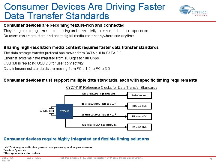
Consumer Devices Are Driving Faster Data Transfer Standards Consumer devices are becoming feature-rich and connected They integrate storage, media processing and connectivity to enhance the user experience So users can create, store and share digital media content anywhere and anytime Sharing high-resolution media content requires faster data transfer standards The data storage transfer protocol has moved from SATA 1. 0 to SATA 3. 0 Ethernet systems have migrated from 10 Gbps to 100 Gbps USB 3. 0 is replacing USB 2. 0 for user connectivity Data interconnect standards are moving from PCIe 1. 0 to PCIe 3. 0 Consumer devices must support multiple data standards, each with specific timing requirements CY 274101 Reference Clocks for Data Transfer Standards 100 -MHz LVDS, 3 -ps RMS Jitter 48 -MHz LVCMOS, 100 -ps CCJ 2 24 MHz SATA 3. 0 Host USB 3. 0 Hub CY 27410 25 -MHz LVCMOS, 100 -ps CCJ 2 100 -MHz HCSL 3, 1 -ps RMS Jitter Ethernet MAC PCIe 3. 0 Hub Consumer devices require highly integrated and flexible timing solutions 1 CY 27410 programmable clock generator can generate up to 12 output frequencies 2 Cycle-to-Cycle Jitter 3 High-speed current steering logic 001 -91135 Rev *D Owner: PAJE High-Performance 4 -PLL Clock Generator New Product Introduction (Customer) 3 a

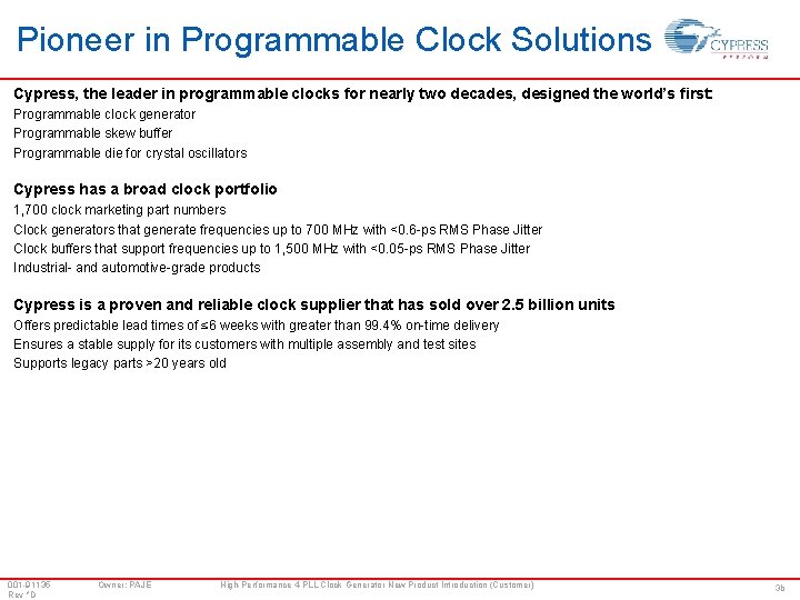
Pioneer in Programmable Clock Solutions Cypress, the leader in programmable clocks for nearly two decades, designed the world’s first: Programmable clock generator Programmable skew buffer Programmable die for crystal oscillators Cypress has a broad clock portfolio 1, 700 clock marketing part numbers Clock generators that generate frequencies up to 700 MHz with <0. 6 -ps RMS Phase Jitter Clock buffers that support frequencies up to 1, 500 MHz with <0. 05 -ps RMS Phase Jitter Industrial- and automotive-grade products Cypress is a proven and reliable clock supplier that has sold over 2. 5 billion units Offers predictable lead times of ≤ 6 weeks with greater than 99. 4% on-time delivery Ensures a stable supply for its customers with multiple assembly and test sites Supports legacy parts >20 years old 001 -91135 Rev *D Owner: PAJE High-Performance 4 -PLL Clock Generator New Product Introduction (Customer) 3 b

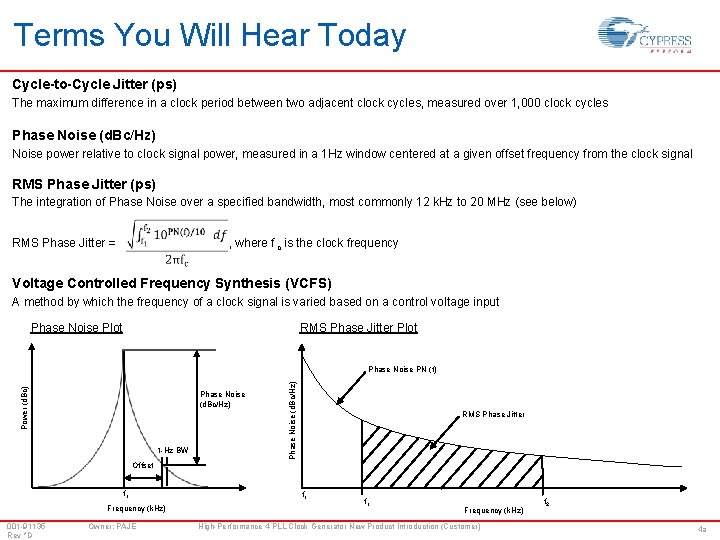
Terms You Will Hear Today Cycle-to-Cycle Jitter (ps) The maximum difference in a clock period between two adjacent clock cycles, measured over 1, 000 clock cycles Phase Noise (d. Bc/Hz) Noise power relative to clock signal power, measured in a 1 Hz window centered at a given offset frequency from the clock signal RMS Phase Jitter (ps) The integration of Phase Noise over a specified bandwidth, most commonly 12 k. Hz to 20 MHz (see below) RMS Phase Jitter = , where f c is the clock frequency Voltage Controlled Frequency Synthesis (VCFS) A method by which the frequency of a clock signal is varied based on a control voltage input Phase Noise Plot RMS Phase Jitter Plot Phase Noise (d. Bc/Hz) 1 -Hz BW Phase Noise (d. Bc/Hz) Power (d. Bc) Phase Noise PN (f) RMS Phase Jitter Offset fc Frequency (k. Hz) 001 -91135 Rev *D Owner: PAJE fc f 1 Frequency (k. Hz) High-Performance 4 -PLL Clock Generator New Product Introduction (Customer) f 2 4 a

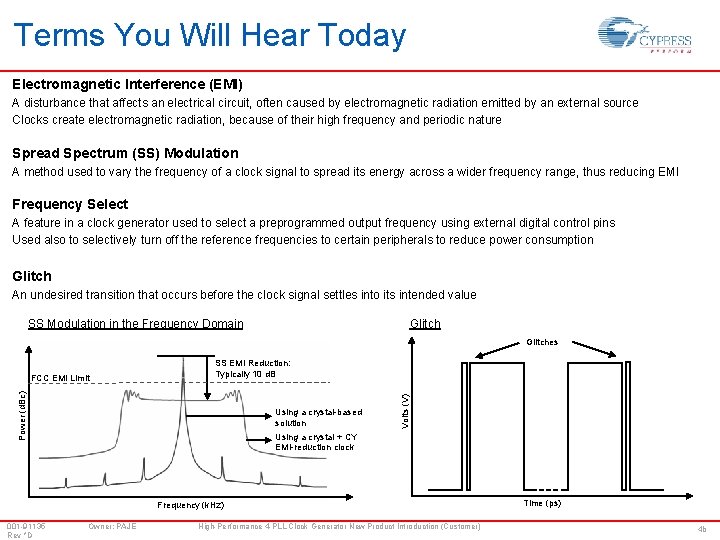
Terms You Will Hear Today Electromagnetic Interference (EMI) A disturbance that affects an electrical circuit, often caused by electromagnetic radiation emitted by an external source Clocks create electromagnetic radiation, because of their high frequency and periodic nature Spread Spectrum (SS) Modulation A method used to vary the frequency of a clock signal to spread its energy across a wider frequency range, thus reducing EMI Frequency Select A feature in a clock generator used to select a preprogrammed output frequency using external digital control pins Used also to selectively turn off the reference frequencies to certain peripherals to reduce power consumption Glitch An undesired transition that occurs before the clock signal settles into its intended value SS Modulation in the Frequency Domain Glitches Using a crystal-based solution Using a crystal + CY EMI-reduction clock Volts (V) Power (d. Bc) FCC EMI Limit SS EMI Reduction: Typically 10 d. B Frequency (k. Hz) 001 -91135 Rev *D Owner: PAJE High-Performance 4 -PLL Clock Generator New Product Introduction (Customer) Time (ps) 4 b

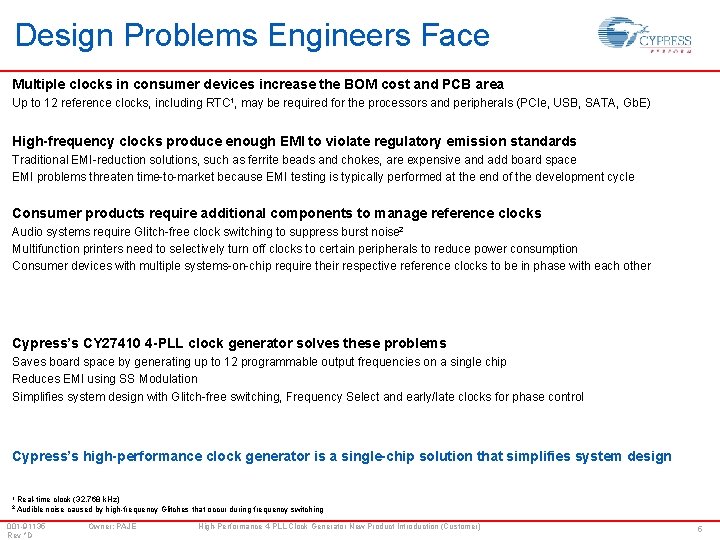
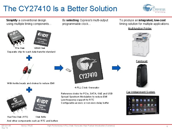
Design Problems Engineers Face Multiple clocks in consumer devices increase the BOM cost and PCB area Up to 12 reference clocks, including RTC 1, may be required for the processors and peripherals (PCIe, USB, SATA, Gb. E) High-frequency clocks produce enough EMI to violate regulatory emission standards Traditional EMI-reduction solutions, such as ferrite beads and chokes, are expensive and add board space EMI problems threaten time-to-market because EMI testing is typically performed at the end of the development cycle Consumer products require additional components to manage reference clocks Audio systems require Glitch-free clock switching to suppress burst noise 2 Multifunction printers need to selectively turn off clocks to certain peripherals to reduce power consumption Consumer devices with multiple systems-on-chip require their respective reference clocks to be in phase with each other Cypress’s CY 27410 4 -PLL clock generator solves these problems Saves board space by generating up to 12 programmable output frequencies on a single chip Reduces EMI using SS Modulation Simplifies system design with Glitch-free switching, Frequency Select and early/late clocks for phase control Cypress’s high-performance clock generator is a single-chip solution that simplifies system design 1 Real-time clock (32. 768 k. Hz) 2 Audible noise caused by high-frequency Glitches that occur during frequency switching 001 -91135 Rev *D Owner: PAJE High-Performance 4 -PLL Clock Generator New Product Introduction (Customer) 5

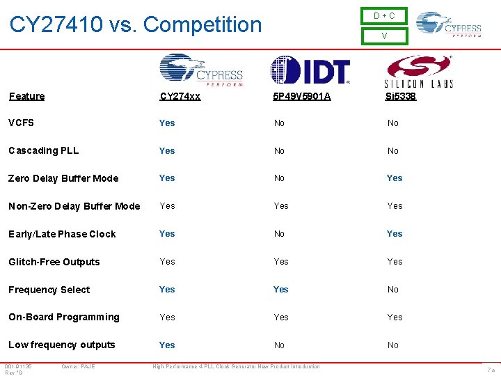
D + C CY 27410 vs. Competition V Feature CY 274 xx 5 P 49 V 5901 A Si 5338 VCFS Yes No No Cascading PLL Yes No No Zero Delay Buffer Mode Yes Non-Zero Delay Buffer Mode Yes Yes Early/Late Phase Clock Yes No Yes Glitch-Free Outputs Yes Yes Frequency Select Yes No On-Board Programming Yes Yes Low frequency outputs Yes No No 001 -91135 Rev *D Owner: PAJE High-Performance 4 -PLL Clock Generator New Product Introduction 7 a

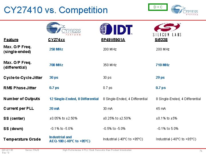
CY 27410 vs. Competition Feature CY 274 xx 5 P 49 V 5901 A D + C Si 5338 Max. O/P Freq. (single-ended) 250 MHz 200 MHz Max. O/P Freq. (differential) 700 MHz 350 MHz 710 MHz Cycle-to-Cycle Jitter 30 ps 29 ps RMS Phase Jitter 0. 7 ps Number of Outputs 12 Single-Ended, 8 Differential 8 Single-Ended, 4 Differential Current per PLL 20 m. A 30 m. A 45 m. A SS (center) ± 0. 05% to ± 2. 50% ± 0. 25% to ± 2. 50% ± 0. 1% to ± 5% SS (down) -0. 1% to -5. 0% -0. 5% to -5. 0% -0. 1% to 5. 0% Temperature Grade Industrial and AEQ-100 (-40ºC to +85ºC) Industrial (-40ºC to +85ºC) 001 -91135 Rev *D Owner: PAJE High-Performance 4 -PLL Clock Generator New Product Introduction 7 b

The CY 27410 Is a Better Solution Simplify a conventional design using multiple timing components… By selecting Cypress’s multi-output programmable clock… To produce an integrated, low-cost timing solution for multiple applications. Multifunction Printer b. E G 10 PCIe Clock 10 Gb. E Clock Separate chip for each data transfer standard Femtocell With ferrite beads and chokes to reduce EMI 4 -PLL Clock Generator Reference clocks for PCIe, SATA, Gb. E and USB Spread Spectrum Modulation to reduce EMI Low-frequency support for RTC Configurable as zero or non-zero delay buffer Real-Time Clock ( RTC) Car Infotainment System Clock Buffer And other components such as RTC and buffers 001 -91135 Rev *D Owner: PAJE High-Performance 4 -PLL Clock Generator New Product Introduction (Customer) 6

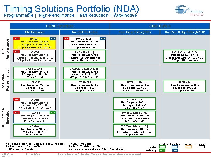
Timing Solutions Portfolio (NDA) Programmable | High-Performance | EMI Reduction | Automotive Clock Generators Non-EMI Reduction NEW Q 115 CY 274 x Max. Frequency: 700 MHz 12 outputs; PCIe 3. 0; 4 PLL 0. 7 -ps RMS Jitter 1; Ind 2; Auto A 3 NEW CY 294 x/ CY 5107 Max. Frequency: 2. 1 GHz 1 output; 40/100 Gb. E; 1 PLL 0. 15 -ps RMS Jitter 1; Ind 2 CY 276 x Max. Frequency: 700 MHz 8 outputs; PCIe 3. 0, 10 Gb. E; 2 PLL 0. 7 -ps RMS Jitter 1; Ind 2; Auto A 3 CY 2 Xx (Fle. XO™) Max. Frequency: 690 MHz 1 output; Frequency Margining 0. 6 -ps RMS Jitter 1; Ind 2 CY 254 x/CY 251 x Max. Frequency: 166 MHz 3 -9 outputs; 1 -4 PLL; I 2 C 100 -ps CCJ 4; Ind 2 CY 2239 x/CY 2238 x Max. Frequency: 200 MHz 3 -6 outputs; 3 -4 PLL; I 2 C 400 -ps CCJ 4; Ind 2; Auto E 5 CY 22800/801 Max. Frequency: 166 MHz 3 outputs; 1 PLL 250 -ps CCJ 4; Ind 2 CY 22050/150 Max. Frequency: 200 MHz 3 -6 outputs; 1 PLL 250 -ps CCJ 4; Ind 2 Standard Performance High Performance EMI Reduction Clock Buffers Zero Delay Buffer (ZDB) Q 315 Application Specific CY 278 x Max. Frequency: 200 MHz 4 outputs; PCIe 3. 0; 1 PLL < 0. 7 -ps RMS Jitter 1; Ind 2; Auto A 3 CY 24293 A Max. Frequency: 200 MHz 2 outputs; 1 PLL; PCIe 1. 1 75 -ps CCJ 4; Auto A 3 CY 2 DLx/DMx/DPx/CPx Max. Frequency: 1. 5 GHz 2 -10 outputs; LVDS, LVPECL, CML 0. 05 -ps RMS Jitter 1; Ind 2 CY 230 x/EP 0 x Max. Frequency: 220 MHz 5 -9 outputs; LVCMOS 22 -ps CCJ 4; Ind 2; Auto A 3 CY 23 S 02/05/08/09/FP 12 Max. Frequency: 200 MHz 2 -12 outputs; Spread Aware 200 -ps CCJ 4; Ind 2 Q 115 CY 2429 x Max. Frequency: 200 MHz 2 -4 outputs; PCIe 1. 1 75 -ps CCJ 4; Ind 2 CY 7 B 99 x (Robo. Clock™) Max. Frequency: 200 MHz 8 -18 outputs; Configurable Skew 50 -ps CCJ 4; Ind 2 1 Integrated phase noise across 12 -k. Hz to 20 -MHz offset 4 Cycle-to-cycle jitter 2 Industrial grade: -40ºC to +85ºC 5 AEC-Q 100: -40ºC to +125ºC 3 AEC-Q 100: -40ºC to +85ºC 6 Automatic clock switching on failure of a clock source 001 -91135 Rev *D Owner: PAJE CY 230 x. NZ Max. Frequency: 133 MHz 4 -18 outputs; LVCMOS 250 -ps CCJ 4; Ind 2 CY 23 FS 04/08 Max. Frequency: 200 MHz 4 -8 outputs; Fail Safe 6 200 -ps CCJ 4; Ind 2 NEW Non-Zero Delay Buffer (NZDB) High-Performance 4 -PLL Clock Generator New Product Introduction (Customer) Production Sampling Development Concept Status Availability QQYY

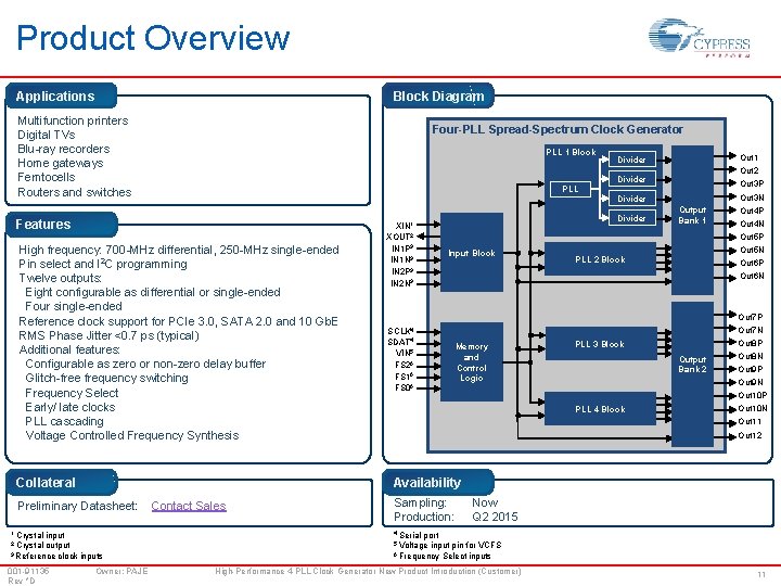
Product Overview Applications Block Diagram Multifunction printers Digital TVs Blu-ray recorders Home gateways Femtocells Routers and switches Four-PLL Spread-Spectrum Clock Generator PLL 1 Block PLL High frequency: 700 -MHz differential, 250 -MHz single-ended Pin select and I 2 C programming Twelve outputs: Eight configurable as differential or single-ended Four single-ended Reference clock support for PCIe 3. 0, SATA 2. 0 and 10 Gb. E RMS Phase Jitter <0. 7 ps (typical) Additional features: Configurable as zero or non-zero delay buffer Glitch-free frequency switching Frequency Select Early/ late clocks PLL cascading Voltage Controlled Frequency Synthesis XIN 1 XOUT 2 IN 1 P 3 IN 1 N 3 IN 2 P 3 IN 2 N 3 Out 3 P Out 3 N Divider Output Bank 1 Out 4 P Out 4 N Out 5 P Input Block Out 5 N PLL 2 Block Out 6 P Out 6 N Out 7 P Out 7 N SCLK 4 SDAT 4 VIN 5 FS 26 FS 16 FS 06 Memory and Control Logic Out 8 P PLL 3 Block Output Bank 2 Out 8 N Out 9 P Out 9 N Out 10 P PLL 4 Block Out 10 N Out 11 Out 12 Collateral Availability Preliminary Datasheet: Contact Sales Sampling: Production: Now Q 2 2015 1 Crystal input 4 Serial port 2 Crystal output 5 Voltage input pin for VCFS 3 Reference clock inputs 6 Frequency Select inputs Owner: PAJE Out 2 Divider Features 001 -91135 Rev *D Out 1 Divider High-Performance 4 -PLL Clock Generator New Product Introduction (Customer) 11

Here’s How to Get Started 1. Visit the Cypress Timing Solutions website: www. cypress. com/gotiming 2. See our roadmap for Timing Solutions: www. cypress. com/go/Timing. Roadmaps 3. Request a preliminary datasheet: Contact Sales 4. Contact us for questions: clocksandbuffers@cypress. com 001 -91135 Rev *D Owner: PAJE High-Performance 4 -PLL Clock Generator New Product Introduction (Customer) 12

APPENDIX 001 -91135 Rev *D Owner: PAJE High-Performance 4 -PLL Clock Generator New Product Introduction (Customer) 15

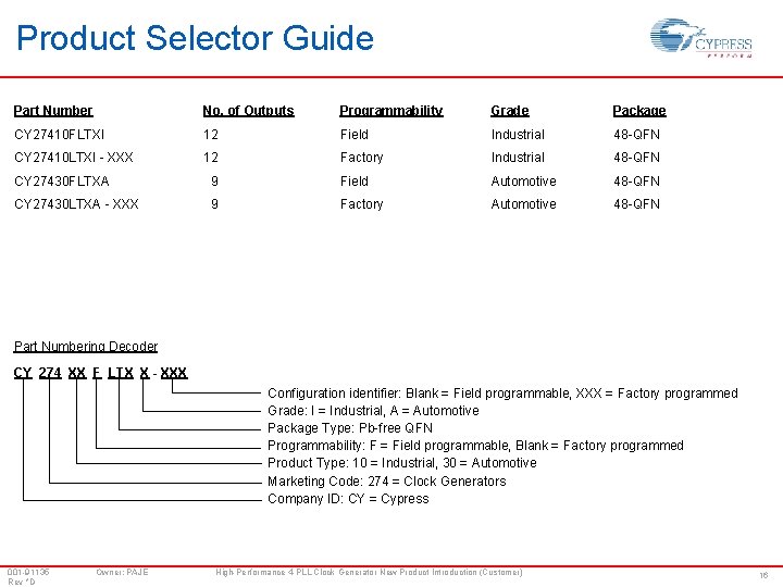
Product Selector Guide Part Number No. of Outputs Programmability Grade Package CY 27410 FLTXI 12 Field Industrial 48 -QFN CY 27410 LTXI - XXX 12 Factory Industrial 48 -QFN CY 27430 FLTXA 9 Field Automotive 48 -QFN CY 27430 LTXA - XXX 9 Factory Automotive 48 -QFN Part Numbering Decoder CY 274 XX F LTX X - XXX Configuration identifier: Blank = Field programmable, XXX = Factory programmed Grade: I = Industrial, A = Automotive Package Type: Pb-free QFN Programmability: F = Field programmable, Blank = Factory programmed Product Type: 10 = Industrial, 30 = Automotive Marketing Code: 274 = Clock Generators Company ID: CY = Cypress 001 -91135 Rev *D Owner: PAJE High-Performance 4 -PLL Clock Generator New Product Introduction (Customer) 16

References and Links Cypress Timing Solutions Website: www. cypress. com/gotiming Timing Solutions Roadmap: www. cypress. com/go/Timing. Roadmaps Product Overview: www. cypress. com/go/CY 27410 Programming and Evaluation Kits: www. cypress. com/go/Timing. Kits Software: www. cypress. com/go/Timing. Software Application Notes: www. cypress. com/go/Timing. App. Notes Contact us for questions: clocksandbuffers@cypress. com 001 -91135 Rev *D Owner: PAJE High-Performance 4 -PLL Clock Generator New Product Introduction (Customer) 18

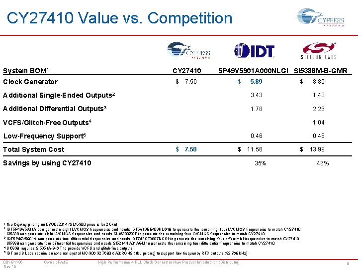
CY 27410 Value vs. Competition System BOM 1 CY 27410 Clock Generator 5 P 49 V 5901 A 000 NLGI SI 5338 M-B-GMR $ 7. 50 $ 5. 89 $ 8. 80 Additional Single-Ended Outputs 2 3. 43 1. 43 Additional Differential Outputs 3 1. 78 2. 26 VCFS/Glitch-Free Outputs 4 1. 04 Low-Frequency Support 5 0. 46 Total System Cost $ 7. 50 $ Savings by using CY 27410 11. 56 0. 46 $ 35% 13. 99 46% 1 1 ku Digikey pricing on 07/30 /2014 (SL 15300 price is for 2. 5 ku) 2 IDT 5 P 49 V 5901 A can generate eight LVCMOS frequencies and needs IDT 5 V 19 EE 403 NLG 18 to generate the remaining four LVCMOS frequencies to match CY 27410 SI 5338 can generate eight LVCMOS frequencies and needs SL 15300 ZCT to generate the remaining four LVCMOS frequencies to match CY 27410 3 IDT 5 P 49 V 5901 A can generate four differential frequencies and needs IDT 74 FCT 3807 DCGI to generate the remaining four differential frequencies to match CY 27410 SI 5338 can generate four differential frequencies and needs SI 52144 -A 01 AGM to generate the remaining four differential frequencies to match CY 27410 4 SI 5338 requires SI 5351 A-B-GT to provide VCFS and glitch-free outputs 5 IDT and Si. Labs require an external crystal MC-306 32. 7680 K-A 0: ROHS (1 ku pricing) to support low-frequency RTC outputs (32. 768 k. Hz) 001 -91135 Rev *D Owner: PAJE High-Performance 4 -PLL Clock Generator New Product Introduction (Distributor) 8