
New Product Introduction 64 Mb to 2 Gb

New Product Introduction: 64 Mb to 2 Gb Parallel Page Mode GL-S NOR Flash Memory Family GL-S = Cypress’s 3. 0 -V, 65 -nm Parallel NOR Flash Memory with Mirror. Bit® 1 Technology The Industry’s Fastest Parallel Page Mode NOR Flash Memory Product Family for High-Performance Systems 1 Cypress Nonvolatile Memory cell technology with two localized electron storage locations to provide two data bits per cell, effectively doubling the NOR Flash Memory density 001 -96834 Rev *A Owner: RYSU/EWOO Tech lead: WIOB 64 Mb to 2 Gb Parallel Page Mode GL-S NOR Flash Memory Family (Customer) Title 1
NOR Flash Memory Terms Nonvolatile Memory (NVM) A memory that retains data even when it is not powered Program Memory A low-latency and high-bandwidth NVM that enables fast execution of CPU instructions Flash Memory An NVM that alters the voltage at which a transistor conducts current by adding or removing electrons to set predefined “ 1” and “ 0” states for a memory cell NOR Flash Memory A Flash Memory with a memory architecture optimized for fast, low-latency random access (vs. fast consecutive address access) Mirror. Bit® Cypress NVM cell technology with two localized electron storage locations to provide two data bits per cell, effectively doubling the NOR Flash Memory density 001 -96834 Rev *A Owner: RYSU/EWOO Tech lead: WIOB 64 Mb to 2 Gb Parallel Page Mode GL-S NOR Flash Memory Family (Customer) Terms of Art 2
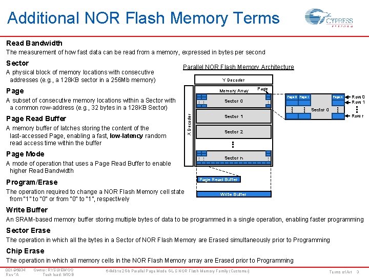
Additional NOR Flash Memory Terms Read Bandwidth The measurement of how fast data can be read from a memory, expressed in bytes per second Sector A physical block of memory locations with consecutive addresses (e. g. , a 128 KB sector in a 256 Mb memory) Parallel NOR Flash Memory Architecture Y Decoder Page Memory Array Row 0 Row 1 X Decoder Page n Sector 0 Row r Sector 2 Sector n A mode of operation that uses a Page Read Buffer to enable higher Read Bandwidth Page 0 Page 1 Sector 1 Page Mode Sector 0 A memory buffer of latches storing the content of the last-accessed Page, enabling a fast, low-latency random read access time within the buffer Page Read Buffer A subset of consecutive memory locations within a Sector with a common row-address (e. g. , 32 bytes in a 128 KB Sector) Page Read Buffer Program/Erase The operation required to change a NOR Flash Memory cell state from “ 1” to “ 0” or from “ 0” to “ 1”, respectively Write Buffer An SRAM-based memory buffer storing multiple bytes of data to be programmed in a single operation, enabling faster programming Sector Erase The operation in which all the bytes in a Sector of NOR Flash Memory are Erased simultaneously prior to Programming Chip Erase The operation in which all memory cells in the NOR Flash Memory array are Erased prior to Programming 001 -96834 Rev *A Owner: RYSU/EWOO Tech lead: WIOB 64 Mb to 2 Gb Parallel Page Mode GL-S NOR Flash Memory Family (Customer) Terms of Art 3

High-Performance Systems Require the Fastest Parallel NOR Flash Memory High-performance systems require parallel Page Mode NOR Flash Memory to access Program Memory as fast as possible Parallel NOR Flash Memory market segments: Automotive Communication Industrial Automation Automotive Infotainment System by BMW Router by Cisco Industrial Controller by Honeywell Designers of high-performance systems in these market segments require NOR Flash Memory with the highest Read Bandwidth, fastest Program time and the fastest Sector Erase time Designers of high-performance systems in these market segments require higher-temperature-range components because they need to shrink enclosures, reducing airflow Designers of high-performance systems require the fastest parallel Page Mode NOR Flash Memory with higher temperature ranges 001 -96834 Rev *A Owner: RYSU/EWOO Tech lead: WIOB 64 Mb to 2 Gb Parallel Page Mode GL-S NOR Flash Memory Family (Customer) Market Vision 4
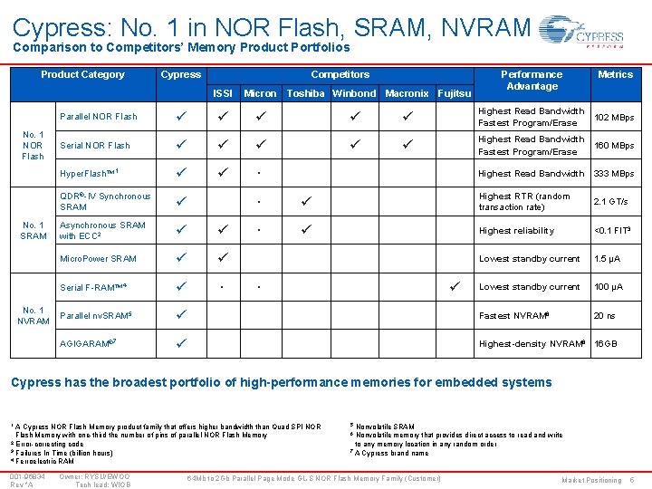
Cypress: No. 1 in NOR Flash, SRAM, NVRAM Comparison to Competitors’ Memory Product Portfolios Product Category Cypress Competitors ISSI No. 1 NOR Flash No. 1 SRAM No. 1 NVRAM Micron Toshiba Winbond Macronix Fujitsu Performance Advantage Metrics Parallel NOR Flash Highest Read Bandwidth 102 MBps Fastest Program/Erase Serial NOR Flash Highest Read Bandwidth 160 MBps Fastest Program/Erase Hyper. Flash™ 1 QDR®-IV Synchronous SRAM Asynchronous SRAM with ECC 2 Micro. Power SRAM Serial F-RAM™ 4 Parallel nv. SRAM 5 AGIGARAM® 7 Highest Read Bandwidth 333 MBps Highest RTR (random transaction rate) 2. 1 GT/s Highest reliability <0. 1 FIT 3 Lowest standby current 1. 5 µA Lowest standby current 100 µA Fastest NVRAM 6 20 ns Highest-density NVRAM 6 16 GB Cypress has the broadest portfolio of high-performance memories for embedded systems A Cypress NOR Flash Memory product family that offers higher bandwidth than Quad SPI NOR Flash Memory with one-third the number of pins of parallel NOR Flash Memory 2 Error-correcting code 3 Failures In Time (billion hours) 4 Ferroelectric RAM 1 001 -96834 Rev *A Owner: RYSU/EWOO Tech lead: WIOB Nonvolatile SRAM Nonvolatile memory that provides direct access to read and write to any memory location in any random order 7 A Cypress brand name 5 6 64 Mb to 2 Gb Parallel Page Mode GL-S NOR Flash Memory Family (Customer) Market Positioning 5
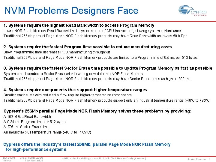
NVM Problems Designers Face 1. Systems require the highest Read Bandwidth to access Program Memory Lower NOR Flash Memory Read Bandwidth delays execution of CPU instructions, slowing system performance Traditional 256 Mb parallel Page Mode NOR Flash Memory products may have Read Bandwidth as low as 58 MBps 2. Systems require the fastest Program time possible to reduce manufacturing costs Slow Programming time decreases PCB manufacturing throughput Traditional 256 Mb parallel Page Mode NOR Flash Memory products are limited to a Program time of 0. 5 ms per 512 bytes 3. Systems require the fastest Sector Erase time possible to update Program Memory as fast as possible Systems must conduct a Sector Erase prior to writing new data into NOR Flash Memory Traditional 256 Mb parallel Page Mode NOR Flash Memory products may have Sector Erase times as high as 800 ms 4. Systems require components that support higher temperature ranges Smaller enclosures with reduced airflow require higher-temperature components Traditional 256 Mb parallel Page Mode NOR Flash Memory products support only an industrial temperature range (-40ºC to +85ºC) Cypress’s 256 Mb parallel Page Mode NOR Flash Memory solves these problems by providing: A 102 -MBps Read Bandwidth A 0. 34 -ms Program time per 512 bytes A 275 -ms Sector Erase time An industrial-plus temperature range (-40ºC to +105ºC) Cypress offers the industry’s fastest 256 Mb, parallel Page Mode NOR Flash Memory for high-performance systems 001 -96834 Rev *A Owner: RYSU/EWOO Tech lead: WIOB 64 Mb to 2 Gb Parallel Page Mode GL-S NOR Flash Memory Family (Customer) Design Problems 6
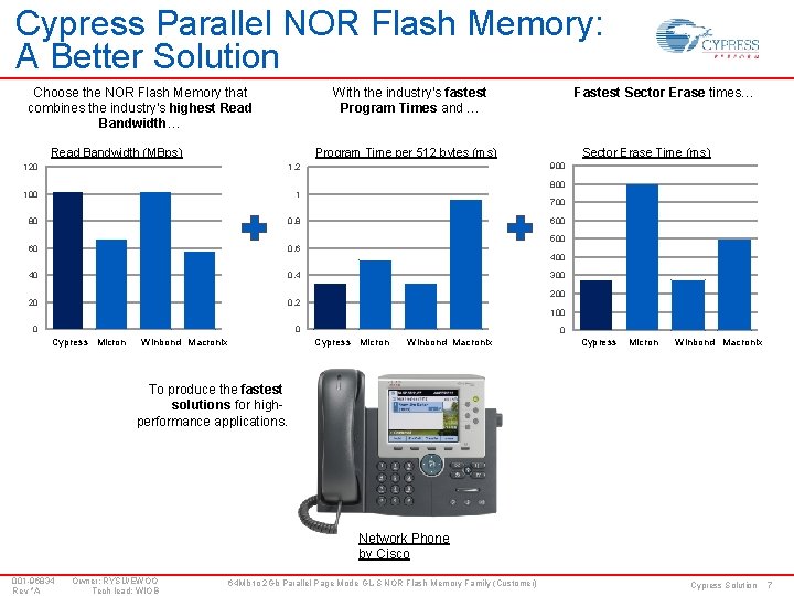
Cypress Parallel NOR Flash Memory: A Better Solution Fastest Sector Erase times… With the industry’s fastest Program Times and … Choose the NOR Flash Memory that combines the industry’s highest Read Bandwidth… Read Bandwidth (MBps) Program Time per 512 bytes (ms) 120 1, 2 100 1 80 0, 8 60 0, 6 40 0, 4 20 0, 2 Sector Erase Time (ms) 900 800 700 600 500 400 300 200 100 0 0 Cypress Micron Winbond Macronix To produce the fastest solutions for highperformance applications. Network Phone by Cisco 001 -96834 Rev *A Owner: RYSU/EWOO Tech lead: WIOB 64 Mb to 2 Gb Parallel Page Mode GL-S NOR Flash Memory Family (Customer) Cypress Solution 7
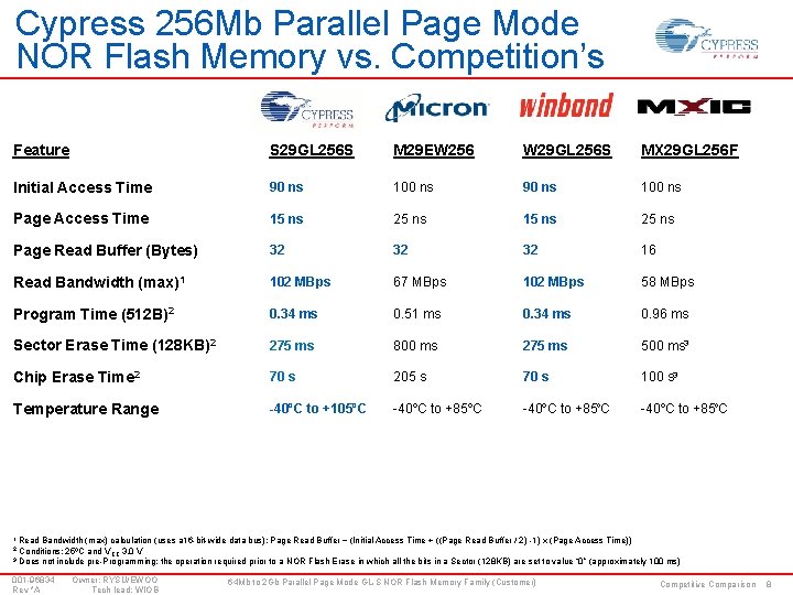
Cypress 256 Mb Parallel Page Mode NOR Flash Memory vs. Competition’s Feature S 29 GL 256 S M 29 EW 256 W 29 GL 256 S MX 29 GL 256 F Initial Access Time 90 ns 100 ns Page Access Time 15 ns 25 ns Page Read Buffer (Bytes) 32 32 32 16 Read Bandwidth (max)1 102 MBps 67 MBps 102 MBps 58 MBps Program Time (512 B)2 0. 34 ms 0. 51 ms 0. 34 ms 0. 96 ms Sector Erase Time (128 KB)2 275 ms 800 ms 275 ms 500 ms 3 Chip Erase Time 2 70 s 205 s 70 s 100 s 3 Temperature Range -40ºC to +105ºC -40ºC to +85ºC 1 Read Bandwidth (max) calculation (uses a 16 -bit-wide data bus): Page Read Buffer ÷ (Initial Access Time + ((Page Read Buffer / 2) -1) x (Page Access Time)) Conditions: 25ºC and V CC 3. 0 V 3 Does not include pre-Programming: the operation required prior to a NOR Flash Erase in which all the bits in a Sector (128 KB) are set to value “ 0” (approximately 100 ms) 2 001 -96834 Rev *A Owner: RYSU/EWOO Tech lead: WIOB 64 Mb to 2 Gb Parallel Page Mode GL-S NOR Flash Memory Family (Customer) Competitive Comparison 8
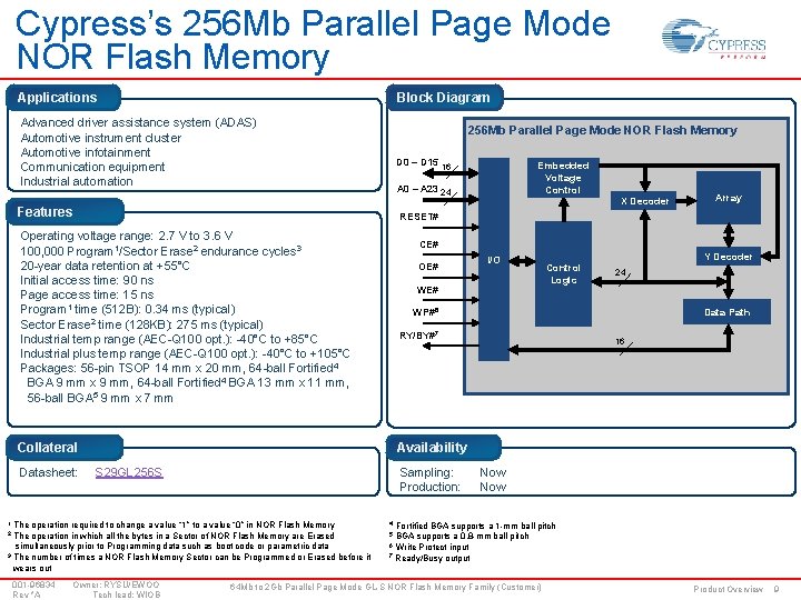
Cypress’s 256 Mb Parallel Page Mode NOR Flash Memory Applications Block Diagram Advanced driver assistance system (ADAS) Automotive instrument cluster Automotive infotainment Communication equipment Industrial automation 256 Mb Parallel Page Mode NOR Flash Memory D 0 – D 15 16 A 0 – A 23 24 Features Array CE# OE# I/O WE# Y Decoder Control Logic 24 Data Path WP#6 RY/BY#7 Collateral 16 Availability S 29 GL 256 S Sampling: Production: The operation required to change a value “ 1” to a value “ 0” in NOR Flash Memory The operation in which all the bytes in a Sector of NOR Flash Memory are Erased simultaneously prior to Programming data such as boot code or parametric data 3 The number of times a NOR Flash Memory Sector can be Programmed or Erased before it wears out 1 4 2 5 001 -96834 Rev *A X Decoder RESET# Operating voltage range: 2. 7 V to 3. 6 V 100, 000 Program 1/Sector Erase 2 endurance cycles 3 20 -year data retention at +55°C Initial access time: 90 ns Page access time: 15 ns Program 1 time (512 B): 0. 34 ms (typical) Sector Erase 2 time (128 KB): 275 ms (typical) Industrial temp range (AEC-Q 100 opt. ): -40°C to +85°C Industrial plus temp range (AEC-Q 100 opt. ): -40°C to +105°C Packages: 56 -pin TSOP 14 mm x 20 mm, 64 -ball Fortified 4 BGA 9 mm x 9 mm, 64 -ball Fortified 4 BGA 13 mm x 11 mm, 56 -ball BGA 5 9 mm x 7 mm Datasheet: Embedded Voltage Control Owner: RYSU/EWOO Tech lead: WIOB Now Fortified BGA supports a 1 -mm ball pitch BGA supports a 0. 8 -mm ball pitch 6 Write Protect input 7 Ready/Busy output 64 Mb to 2 Gb Parallel Page Mode GL-S NOR Flash Memory Family (Customer) Product Overview 9
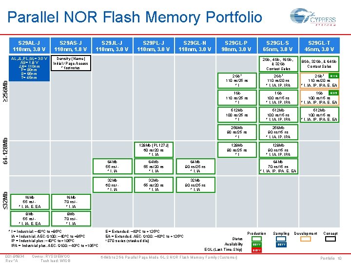
Parallel NOR Flash Memory Portfolio S 29 AS-J 110 nm, 1. 8 V AL, JL, PL, GL= 3. 0 V AS= 1. 8 V J, N= 110 nm P= 90 nm S= 65 nm T= 45 nm Density (Name) Initial / Page Access * footnotes S 29 JL-J 110 nm, 3. 0 V S 29 PL-J 110 nm, 3. 0 V S 29 GL-N 110 nm, 3. 0 V ≤ 32 Mb 64 -128 Mb ≥ 256 Mb S 29 AL-J 110 nm, 3. 0 V 128 Mb (PL 127 J) 60 ns/20 ns * I, IA 16 Mb 55 ns/-* I, IA, E, EA 16 Mb 70 ns/-* I, IA 8 Mb 55 ns/-* I, IA, E, EA 8 Mb 70 ns/-* I, IA * I = Industrial: − 40ºC to +85ºC IA = Industrial, AEC-Q 100: − 40ºC to +85ºC IP = Industrial plus: − 40ºC to +105ºC IPA = Industrial plus, AEC-Q 100: − 40ºC to +105ºC 001 -96834 Rev *A Owner: RYSU/EWOO Tech lead: WIOB 64 Mb 55 ns/-* I, IA 64 Mb 55 ns/20 ns * I, IA 64 Mb 90 ns/25 ns * I, IA 32 Mb 60 ns/-* I, IA 32 Mb 55 ns/20 ns * I, IA 32 Mb 90 ns/25 ns * I, IA E = Extended: − 40ºC to +125ºC EA = Extended, AEC-Q 100: − 40ºC to +125ºC 1 S 70 series (stacked die) S 29 GL-P 90 nm, 3. 0 V S 29 GL-S 65 nm, 3. 0 V S 29 GL-T 45 nm, 3. 0 V 2 Gb, 4 Gb, 16 Gb, & 32 Gb Contact Sales 8 Gb, 32 Gb, & 64 Gb Contact Sales 2 Gb 1 110 ns/25 ns *I 2 Gb 1 110 ns/20 ns * I, IA, IPA Q 116 2 Gb 1 110 ns/20 ns * I, IA, IPA, E, EA 1 Gb 110 ns/25 ns *I 1 Gb 100 ns/15 ns * I, IA, IPA Q 315 1 Gb 100 ns/15 ns * I, IA, IPA, E, EA 512 Mb 100 ns/25 ns *I 512 Mb 100 ns/15 ns * I, IA, IP, IPA, E, EA 256 Mb 90 ns/25 ns *I 256 Mb 90 ns/15 ns * I, IA, IPA 128 Mb 90 ns/25 ns *I 128 Mb 90 ns/15 ns * I, IA, IPA Status Availability EOL (Last-Time-Ship) 64 Mb to 2 Gb Parallel Page Mode GL-S NOR Flash Memory Family (Customer) 64 Mb 70 ns/15 ns * I, IA, IPA, E, EA Production Sampling QQYY Development Concept QQYY Portfolio 10
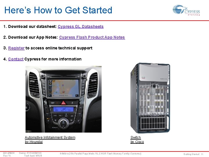
Here’s How to Get Started 1. Download our datasheet: Cypress GL Datasheets 2. Download our App Notes: Cypress Flash Product App Notes 3. Register to access online technical support 4. Contact Cypress for more information Automotive Infotainment System by Hyundai 001 -96834 Rev *A Owner: RYSU/EWOO Tech lead: WIOB Switch by Cisco 64 Mb to 2 Gb Parallel Page Mode GL-S NOR Flash Memory Family (Customer) Getting Started 11

APPENDIX 001 -96834 Rev *A Owner: RYSU/EWOO Tech lead: WIOB 64 Mb to 2 Gb Parallel Page Mode GL-S NOR Flash Memory Family (Customer) Appendix 12
References and Links S 70 GL 02 GS datasheet: 2 Gb NOR Flash Memory S 29 GL-S Family datasheet: 128 Mb – 1 Gb NOR Flash Memory S 29 GL 064 S datasheet: 64 Mb NOR Flash Memory App note: S 29 GL-S Page Mode Accesses App note: S 29 GL-S Page Read Mode – Reducing Startup Time Website: Cypress GL NOR Flash Memory to learn more Design models: IBIS and Verilog models to simplify your design Drivers and software: To accelerate your design cycle Cross reference guide: To see how Cypress stacks up with the competition Cross reference tool: To easily replace the competitor’s parallel NOR Flash Memory Hardware development tools: Kits, cards, boards to simplify your design Product selector guide: To choose the correct Cypress parallel NOR product Product roadmap: Contact Sales 001 -96834 Rev *A Owner: RYSU/EWOO Tech lead: WIOB 64 Mb to 2 Gb Parallel Page Mode GL-S NOR Flash Memory Family (Customer) References and Links 13
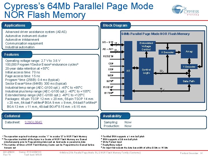
Cypress’s 64 Mb Parallel Page Mode NOR Flash Memory Applications Block Diagram Advanced driver assistance system (ADAS) Automotive instrument cluster Automotive infotainment Communication equipment Industrial automation 64 Mb Parallel Page Mode NOR Flash Memory D 0 – D 15 16 A 0 – A 21 22 Features Array CE# OE# Y Decoder I/O WE# Control Logic 22 Data Path WP#6 RY/BY#7 16 BYTE#8 Collateral Availability S 29 GL 064 S Sampling: Production: The operation required to change a value “ 1” to a value “ 0” in NOR Flash Memory The operation in which all the bytes in a Sector of NOR Flash Memory are Erased simultaneously prior to Programming data such as boot code or parametric data 3 The number of times a NOR Flash Memory Sector can be Programmed or Erased before it wears out 4 2 5 Owner: RYSU/EWOO Tech lead: WIOB Now Fortified BGA supports a 1 -mm ball pitch BGA supports a 0. 8 -mm ball pitch 6 Write Protect input 7 Ready/Busy output 8 An input that selects the data bus width of either 8 bits or 16 bits 1 001 -96834 Rev *A X Decoder RESET# Operating voltage range: 2. 7 V to 3. 6 V 100, 000 Program 1/Sector Erase 2 endurance cycles 3 20 -year data retention at +55°C Initial access time: 70 ns Page access time: 15 ns Program 1 time (256 B): 0. 4 ms (typical) Sector Erase 2 time (64 KB): 300 ms (typical) Industrial temp range (AEC-Q 100 opt. ): -40°C to +85°C Industrial plus temp range (AEC-Q 100 opt. ): -40°C to +105°C Extended temp range (AEC-Q 100 opt. ): -40°C to +125°C Packages: 48 -pin TSOP 12 mm x 20 mm, 56 -pin TSOP 14 mm x 20 mm, 64 -ball Fortified 4 BGA 9 mm x 9 mm, 64 -ball Fortified 4 BGA 13 mm x 11 mm, 48 -ball BGA 5 8. 15 mm x 6. 15 mm Datasheet: Embedded Voltage Control 64 Mb to 2 Gb Parallel Page Mode GL-S NOR Flash Memory Family (Customer) Product Overview 14
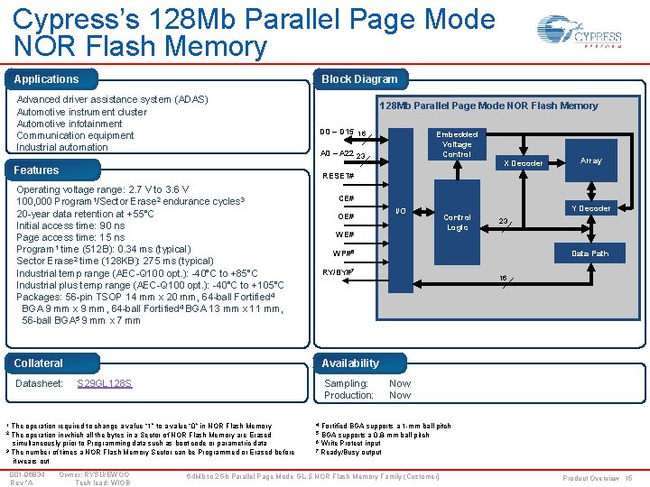
Cypress’s 128 Mb Parallel Page Mode NOR Flash Memory Applications Block Diagram Advanced driver assistance system (ADAS) Automotive instrument cluster Automotive infotainment Communication equipment Industrial automation 128 Mb Parallel Page Mode NOR Flash Memory D 0 – D 15 16 A 0 – A 22 23 Features Array CE# OE# I/O WE# Y Decoder Control Logic 23 Data Path WP#6 RY/BY#7 Collateral 16 Availability S 29 GL 128 S Sampling: Production: The operation required to change a value “ 1” to a value “ 0” in NOR Flash Memory The operation in which all the bytes in a Sector of NOR Flash Memory are Erased simultaneously prior to Programming data such as boot code or parametric data 3 The number of times a NOR Flash Memory Sector can be Programmed or Erased before it wears out 4 2 5 Owner: RYSU/EWOO Tech lead: WIOB Now Fortified BGA supports a 1 -mm ball pitch BGA supports a 0. 8 -mm ball pitch 6 Write Protect input 7 Ready/Busy output 1 001 -96834 Rev *A X Decoder RESET# Operating voltage range: 2. 7 V to 3. 6 V 100, 000 Program 1/Sector Erase 2 endurance cycles 3 20 -year data retention at +55°C Initial access time: 90 ns Page access time: 15 ns Program 1 time (512 B): 0. 34 ms (typical) Sector Erase 2 time (128 KB): 275 ms (typical) Industrial temp range (AEC-Q 100 opt. ): -40°C to +85°C Industrial plus temp range (AEC-Q 100 opt. ): -40°C to +105°C Packages: 56 -pin TSOP 14 mm x 20 mm, 64 -ball Fortified 4 BGA 9 mm x 9 mm, 64 -ball Fortified 4 BGA 13 mm x 11 mm, 56 -ball BGA 5 9 mm x 7 mm Datasheet: Embedded Voltage Control 64 Mb to 2 Gb Parallel Page Mode GL-S NOR Flash Memory Family (Customer) Product Overview 15
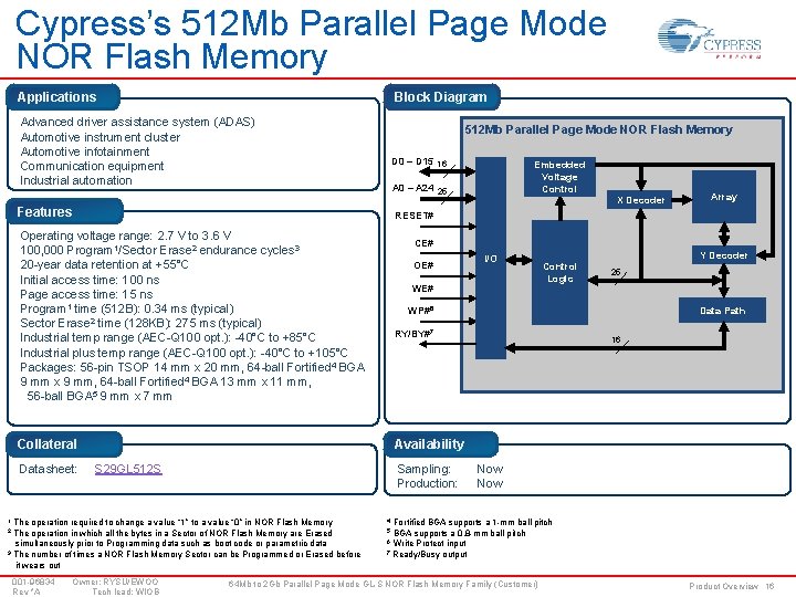
Cypress’s 512 Mb Parallel Page Mode NOR Flash Memory Applications Block Diagram Advanced driver assistance system (ADAS) Automotive instrument cluster Automotive infotainment Communication equipment Industrial automation 512 Mb Parallel Page Mode NOR Flash Memory D 0 – D 15 16 A 0 – A 24 25 Features Array CE# OE# I/O WE# Y Decoder Control Logic 25 Data Path WP#6 RY/BY#7 Collateral 16 Availability S 29 GL 512 S Sampling: Production: The operation required to change a value “ 1” to a value “ 0” in NOR Flash Memory The operation in which all the bytes in a Sector of NOR Flash Memory are Erased simultaneously prior to Programming data such as boot code or parametric data 3 The number of times a NOR Flash Memory Sector can be Programmed or Erased before it wears out 4 2 5 Owner: RYSU/EWOO Tech lead: WIOB Now Fortified BGA supports a 1 -mm ball pitch BGA supports a 0. 8 -mm ball pitch 6 Write Protect input 7 Ready/Busy output 1 001 -96834 Rev *A X Decoder RESET# Operating voltage range: 2. 7 V to 3. 6 V 100, 000 Program 1/Sector Erase 2 endurance cycles 3 20 -year data retention at +55°C Initial access time: 100 ns Page access time: 15 ns Program 1 time (512 B): 0. 34 ms (typical) Sector Erase 2 time (128 KB): 275 ms (typical) Industrial temp range (AEC-Q 100 opt. ): -40°C to +85°C Industrial plus temp range (AEC-Q 100 opt. ): -40°C to +105°C Packages: 56 -pin TSOP 14 mm x 20 mm, 64 -ball Fortified 4 BGA 9 mm x 9 mm, 64 -ball Fortified 4 BGA 13 mm x 11 mm, 56 -ball BGA 5 9 mm x 7 mm Datasheet: Embedded Voltage Control 64 Mb to 2 Gb Parallel Page Mode GL-S NOR Flash Memory Family (Customer) Product Overview 16
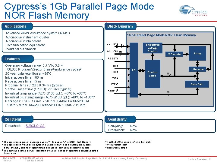
Cypress’s 1 Gb Parallel Page Mode NOR Flash Memory Applications Block Diagram Advanced driver assistance system (ADAS) Automotive instrument cluster Automotive infotainment Communication equipment Industrial automation 1 Gb Parallel Page Mode NOR Flash Memory D 0 – D 15 16 A 0 – A 25 26 Operating voltage range: 2. 7 V to 3. 6 V 100, 000 Program 1/Sector Erase 2 endurance cycles 3 20 -year data retention at +55°C Initial access time: 100 ns Page access time: 15 ns Program 1 time (512 B): 0. 34 ms (typical) Sector Erase 2 time (128 KB): 275 ms (typical) Industrial temp range (AEC-Q 100 opt. ): -40°C to +85°C Industrial plus temp range (AEC-Q 100 opt. ): -40°C to +105°C Packages: TSOP 14 mm x 20 mm, 64 -ball Fortified 4 BGA 9 mm x 9 mm, 64 -ball Fortified 4 BGA 13 mm x 11 mm Array CE# OE# I/O WE# Y Decoder Control Logic 26 Data Path WP#5 RY/BY#6 Collateral 16 Availability S 29 GL 01 GS Sampling: Production: The operation required to change a value “ 1” to a value “ 0” in NOR Flash Memory The operation in which all the bytes in a Sector of NOR Flash Memory are Erased simultaneously prior to Programming data such as boot code or parametric data 3 The number of times a NOR Flash Memory Sector can be Programmed or Erased before it wears out 4 2 5 Owner: RYSU/EWOO Tech lead: WIOB Now Fortified BGA supports a 1 -mm ball pitch Write Protect input 6 Ready/Busy output 1 001 -96834 Rev *A X Decoder RESET# Features Datasheet: Embedded Voltage Control 64 Mb to 2 Gb Parallel Page Mode GL-S NOR Flash Memory Family (Customer) Product Overview 17
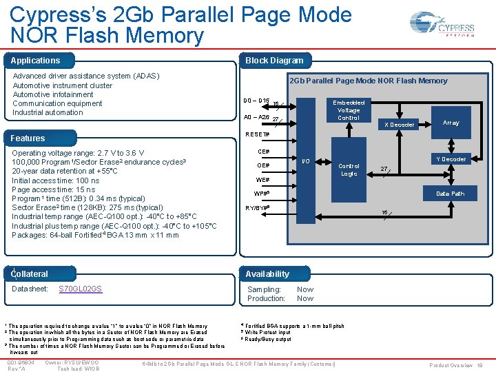
Cypress’s 2 Gb Parallel Page Mode NOR Flash Memory Applications Block Diagram Advanced driver assistance system (ADAS) Automotive instrument cluster Automotive infotainment Communication equipment Industrial automation 2 Gb Parallel Page Mode NOR Flash Memory D 0 – D 15 16 A 0 – A 26 27 Array CE# Operating voltage range: 2. 7 V to 3. 6 V 100, 000 Program 1/Sector Erase 2 endurance cycles 3 20 -year data retention at +55°C Initial access time: 100 ns Page access time: 15 ns Program 1 time (512 B): 0. 34 ms (typical) Sector Erase 2 time (128 KB): 275 ms (typical) Industrial temp range (AEC-Q 100 opt. ): -40°C to +85°C Industrial plus temp range (AEC-Q 100 opt. ): -40°C to +105°C Packages: 64 -ball Fortified 4 BGA 13 mm x 11 mm OE# I/O WE# Y Decoder Control Logic 27 Data Path WP#5 RY/BY#6 Collateral 16 Availability S 70 GL 02 GS Sampling: Production: The operation required to change a value “ 1” to a value “ 0” in NOR Flash Memory The operation in which all the bytes in a Sector of NOR Flash Memory are Erased simultaneously prior to Programming data such as boot code or parametric data 3 The number of times a NOR Flash Memory Sector can be Programmed or Erased before it wears out 4 2 5 Owner: RYSU/EWOO Tech lead: WIOB Now Fortified BGA supports a 1 -mm ball pitch Write Protect input 6 Ready/Busy output 1 001 -96834 Rev *A X Decoder RESET# Features Datasheet: Embedded Voltage Control 64 Mb to 2 Gb Parallel Page Mode GL-S NOR Flash Memory Family (Customer) Product Overview 18
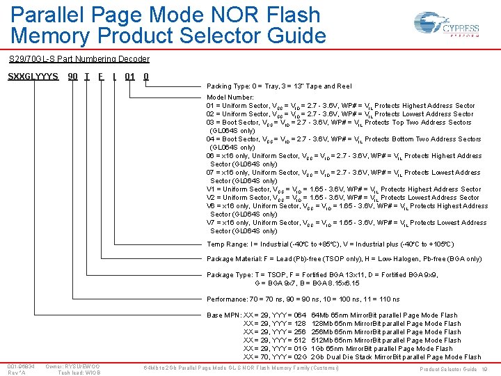
Parallel Page Mode NOR Flash Memory Product Selector Guide S 29/70 GL-S Part Numbering Decoder SXXGLYYYS 90 T F I 01 0 Packing Type: 0 = Tray, 3 = 13” Tape and Reel Model Number: 01 = Uniform Sector, VCC = VIO = 2. 7 - 3. 6 V, WP# = VIL Protects Highest Address Sector 02 = Uniform Sector, VCC = VIO = 2. 7 - 3. 6 V, WP# = VIL Protects Lowest Address Sector 03 = Boot Sector, VCC = VIO = 2. 7 - 3. 6 V, WP# = VIL Protects Top Two Address Sectors (GL 064 S only) 04 = Boot Sector, VCC = VIO = 2. 7 - 3. 6 V, WP# = VIL Protects Bottom Two Address Sectors (GL 064 S only) 06 = x 16 only, Uniform Sector, VCC = VIO = 2. 7 - 3. 6 V, WP# = VIL Protects Highest Address Sector (GL 064 S only) 07 = x 16 only, Uniform Sector, VCC = VIO = 2. 7 - 3. 6 V, WP# = VIL Protects Lowest Address Sector (GL 064 S only) V 1 = Uniform Sector, VCC = VIO = 1. 65 - 3. 6 V, WP# = VIL Protects Highest Address Sector V 2 = Uniform Sector, VCC = VIO = 1. 65 - 3. 6 V, WP# = VIL Protects Lowest Address Sector V 6 = x 16 only, Uniform Sector, VCC = VIO = 1. 65 - 3. 6 V, WP# = VIL Protects Highest Address Sector (GL 064 S only) V 7 = x 16 only, Uniform Sector, VCC = VIO = 1. 65 - 3. 6 V, WP# = VIL Protects Lowest Address Sector (GL 064 S only) Temp Range: I = Industrial (-40ºC to +85ºC), V = Industrial plus (-40ºC to +105ºC) Package Material: F = Lead (Pb)-free (TSOP only), H = Low-Halogen, Pb-free (BGA only) Package Type: T = TSOP, F = Fortified BGA 13 x 11, D = Fortified BGA 9 x 9, G = BGA 9 x 7, B = BGA 8. 15 x 6. 15 Performance: 70 = 70 ns, 90 = 90 ns, 10 = 100 ns, 11 = 110 ns Base MPN: XX = 29, YYY = 064 XX = 29, YYY = 128 XX = 29, YYY = 256 XX = 29, YYY = 512 XX = 29, YYY = 01 G XX = 70, YYY = 02 G 001 -96834 Rev *A Owner: RYSU/EWOO Tech lead: WIOB 64 Mb 65 nm Mirror. Bit parallel Page Mode Flash 128 Mb 65 nm Mirror. Bit parallel Page Mode Flash 256 Mb 65 nm Mirror. Bit parallel Page Mode Flash 512 Mb 65 nm Mirror. Bit parallel Page Mode Flash 1 Gb 65 nm Mirror. Bit parallel Page Mode Flash 2 Gb Dual Die Stack Mirror. Bit parallel Page Mode Flash 64 Mb to 2 Gb Parallel Page Mode GL-S NOR Flash Memory Family (Customer) Product Selector Guide 19
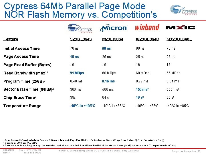
Cypress 64 Mb Parallel Page Mode NOR Flash Memory vs. Competition’s Feature S 29 GL 064 S M 29 EW 064 W 29 GL 064 C MX 29 GL 640 E Initial Access Time 70 ns 60 ns 90 ns 70 ns Page Access Time 15 ns 25 ns Page Read Buffer (Bytes) 16 16 Read Bandwidth (max)1 91 MBps 68 MBps 60 MBps 65 MBps Program Time (256 B)2 0. 40 ms 0. 16 ms 0. 77 ms 0. 64 ms Sector Erase Time (64 KB)2 300 ms 500 ms 150 ms 3 500 ms 3 Chip Erase Time 2 38 s 64 s 19 s 3 60 s 3 Temperature Range -40ºC to +105ºC -40ºC to +85ºC 1 Read Bandwidth (max) calculation (uses a 16 -bit-wide data bus): Page Read Buffer ÷ (Initial Access Time + ((Page Read Buffer / 2) -1) x (Page Access Time)) Conditions: 25ºC and V CC 3. 0 V 3 Does not include pre-Programming: the operation required prior to a NOR Flash Erase in which all the bits in a Sector (64 KB) are set to value “ 0” (approximately 100 ms) 2 001 -96834 Rev *A Owner: RYSU/EWOO Tech lead: WIOB 64 Mb to 2 Gb Parallel Page Mode GL-S NOR Flash Memory Family (Customer) Competitive Comparison 20
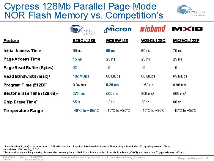
Cypress 128 Mb Parallel Page Mode NOR Flash Memory vs. Competition’s Feature S 29 GL 128 S M 29 EW 128 W 29 GL 128 C MX 29 GL 128 F Initial Access Time 90 ns 60 ns 90 ns 70 ns Page Access Time 15 ns 25 ns Page Read Buffer (Bytes) 32 16 16 16 Read Bandwidth (max)1 102 MBps 68 MBps 60 MBps 65 MBps Program Time (512 B)2 0. 34 ms 0. 28 ms 1. 53 ms 0. 96 ms Sector Erase Time (128 KB)2 275 ms 500 ms 3 Chip Erase Time 2 35 s 131 s 38 s 3 60 s 3 Temperature Range -40ºC to +105ºC -40ºC to +85ºC 1 Read Bandwidth (max) calculation (uses a 16 -bit-wide data bus): Page Read Buffer ÷ (Initial Access Time + ((Page Read Buffer / 2) -1) x (Page Access Time)) Conditions: 25ºC and V CC 3. 0 V 3 Does not include pre-Programming: the operation required prior to a NOR Flash Erase in which all the bits in a Sector (128 KB) are set to value “ 0” (approximately 100 ms) 2 001 -96834 Rev *A Owner: RYSU/EWOO Tech lead: WIOB 64 Mb to 2 Gb Parallel Page Mode GL-S NOR Flash Memory Family (Customer) Competitive Comparison 21
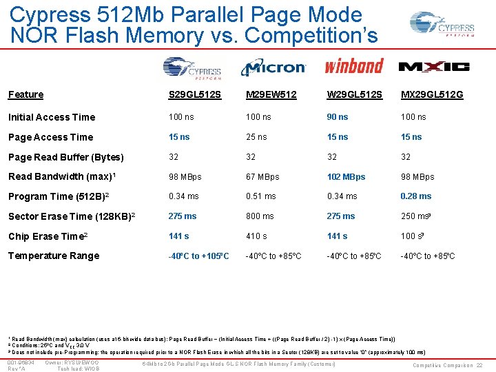
Cypress 512 Mb Parallel Page Mode NOR Flash Memory vs. Competition’s Feature S 29 GL 512 S M 29 EW 512 W 29 GL 512 S MX 29 GL 512 G Initial Access Time 100 ns 90 ns 100 ns Page Access Time 15 ns 25 ns 15 ns Page Read Buffer (Bytes) 32 32 Read Bandwidth (max)1 98 MBps 67 MBps 102 MBps 98 MBps Program Time (512 B)2 0. 34 ms 0. 51 ms 0. 34 ms 0. 28 ms Sector Erase Time (128 KB)2 275 ms 800 ms 275 ms 250 ms 3 Chip Erase Time 2 141 s 410 s 141 s 100 s 3 Temperature Range -40ºC to +105ºC -40ºC to +85ºC 1 Read Bandwidth (max) calculation (uses a 16 -bit-wide data bus): Page Read Buffer ÷ (Initial Access Time + ((Page Read Buffer / 2) -1) x (Page Access Time)) Conditions: 25ºC and V CC 3. 0 V 3 Does not include pre-Programming: the operation required prior to a NOR Flash Erase in which all the bits in a Sector (128 KB) are set to value “ 0” (approximately 100 ms) 2 001 -96834 Rev *A Owner: RYSU/EWOO Tech lead: WIOB 64 Mb to 2 Gb Parallel Page Mode GL-S NOR Flash Memory Family (Customer) Competitive Comparison 22
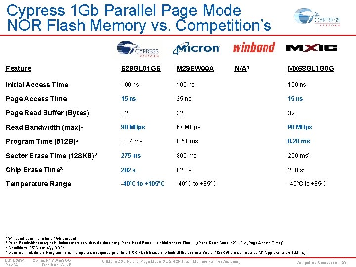
Cypress 1 Gb Parallel Page Mode NOR Flash Memory vs. Competition’s Feature S 29 GL 01 GS M 29 EW 00 A N/A 1 MX 68 GL 1 G 0 G Initial Access Time 100 ns Page Access Time 15 ns 25 ns 15 ns Page Read Buffer (Bytes) 32 32 32 Read Bandwidth (max)2 98 MBps 67 MBps 98 MBps Program Time (512 B)3 0. 34 ms 0. 51 ms 0. 28 ms Sector Erase Time (128 KB)3 275 ms 800 ms 250 ms 4 Chip Erase Time 3 282 s 820 s 200 s 4 Temperature Range -40ºC to +105ºC -40ºC to +85ºC Winbond does not offer a 1 Gb product Bandwidth (max) calculation (uses a 16 -bit-wide data bus): Page Read Buffer ÷ (Initial Access Time + ((Page Read Buffer / 2) -1) x (Page Access Time)) 3 Conditions: 25ºC and V CC 3. 0 V 4 Does not include pre-Programming: the operation required prior to a NOR Flash Erase in which all the bits in a Sector (128 KB) are set to value “ 0” (approximately 100 ms) 1 2 Read 001 -96834 Rev *A Owner: RYSU/EWOO Tech lead: WIOB 64 Mb to 2 Gb Parallel Page Mode GL-S NOR Flash Memory Family (Customer) Competitive Comparison 23
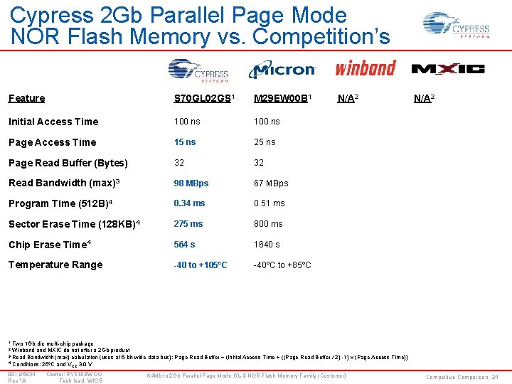
Cypress 2 Gb Parallel Page Mode NOR Flash Memory vs. Competition’s Feature S 70 GL 02 GS 1 M 29 EW 00 B 1 Initial Access Time 100 ns Page Access Time 15 ns 25 ns Page Read Buffer (Bytes) 32 32 Read Bandwidth (max)3 98 MBps 67 MBps Program Time (512 B)4 0. 34 ms 0. 51 ms Sector Erase Time (128 KB)4 275 ms 800 ms Chip Erase Time 4 564 s 1640 s Temperature Range -40 to +105ºC -40ºC to +85ºC N/A 2 Two 1 Gb die multi-chip package Winbond and MXIC do not offer a 2 Gb product 3 Read Bandwidth (max) calculation (uses a 16 -bit-wide data bus): Page Read Buffer ÷ (Initial Access Time + ((Page Read Buffer / 2) -1) x (Page Access Time)) 4 Conditions: 25ºC and V CC 3. 0 V 1 2 001 -96834 Rev *A Owner: RYSU/EWOO Tech lead: WIOB 64 Mb to 2 Gb Parallel Page Mode GL-S NOR Flash Memory Family (Customer) Competitive Comparison 24
- Slides: 24