New Materials for the Gate Stack of MOSTransistors
![Potential High-K materials Ref [5] Which one of them is appropriate? ? Dielectric constant Potential High-K materials Ref [5] Which one of them is appropriate? ? Dielectric constant](https://slidetodoc.com/presentation_image_h2/5cbe625a5326c336cf7538444fb5b5df/image-21.jpg)
![Surface Phonon Limited Mobility Ref [7] Ref [8] New Materials for the Gate Stack Surface Phonon Limited Mobility Ref [7] Ref [8] New Materials for the Gate Stack](https://slidetodoc.com/presentation_image_h2/5cbe625a5326c336cf7538444fb5b5df/image-43.jpg)
![References [1] R. Shireen, et al. , "Influence of polysilicon-gate depletion on the subthreshold References [1] R. Shireen, et al. , "Influence of polysilicon-gate depletion on the subthreshold](https://slidetodoc.com/presentation_image_h2/5cbe625a5326c336cf7538444fb5b5df/image-49.jpg)
![References [6] R. Chau et al. , “Advanced metal gate/high-_ dielectric stacks for high References [6] R. Chau et al. , “Advanced metal gate/high-_ dielectric stacks for high](https://slidetodoc.com/presentation_image_h2/5cbe625a5326c336cf7538444fb5b5df/image-50.jpg)
- Slides: 51

New Materials for the Gate Stack of MOS-Transistors Presented By: Ashesh Jain Tutor: Dr. Nandita Das Gupta Indian Institute of Technology, Delhi 1

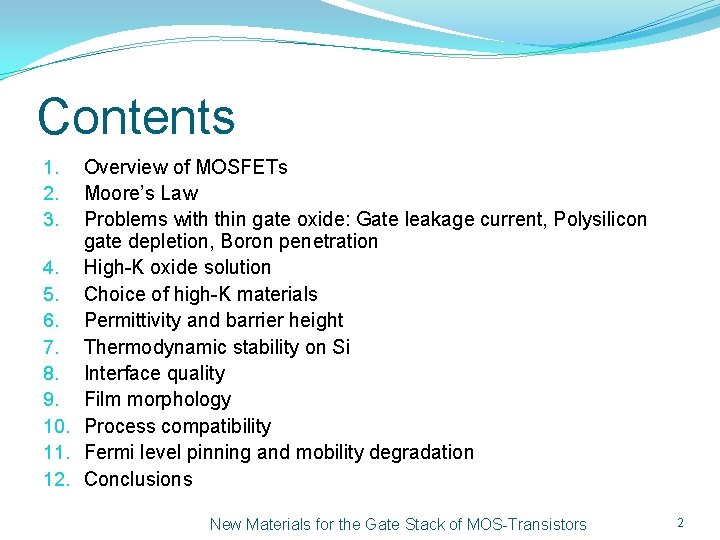
Contents Overview of MOSFETs Moore’s Law Problems with thin gate oxide: Gate leakage current, Polysilicon gate depletion, Boron penetration 4. High-K oxide solution 5. Choice of high-K materials 6. Permittivity and barrier height 7. Thermodynamic stability on Si 8. Interface quality 9. Film morphology 10. Process compatibility 11. Fermi level pinning and mobility degradation 12. Conclusions 1. 2. 3. New Materials for the Gate Stack of MOS-Transistors 2

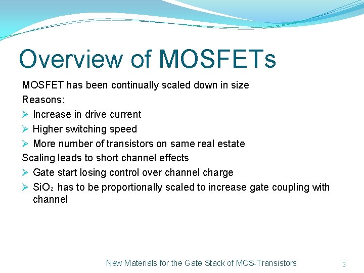
Overview of MOSFETs MOSFET has been continually scaled down in size Reasons: Ø Increase in drive current Ø Higher switching speed Ø More number of transistors on same real estate Scaling leads to short channel effects Ø Gate start losing control over channel charge Ø Si. O₂ has to be proportionally scaled to increase gate coupling with channel New Materials for the Gate Stack of MOS-Transistors 3

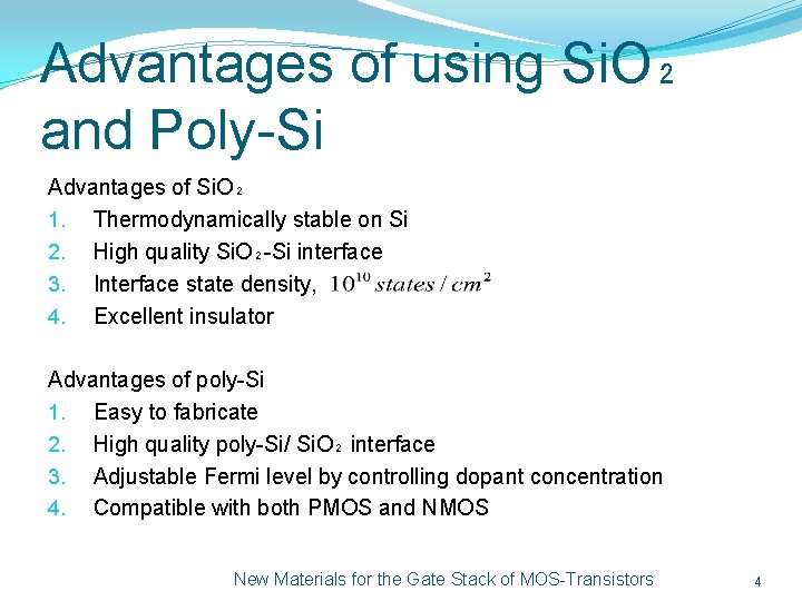
Advantages of using Si. O₂ and Poly-Si Advantages of Si. O₂ 1. Thermodynamically stable on Si 2. High quality Si. O₂-Si interface 3. Interface state density, 4. Excellent insulator Advantages of poly-Si 1. Easy to fabricate 2. High quality poly-Si/ Si. O₂ interface 3. Adjustable Fermi level by controlling dopant concentration 4. Compatible with both PMOS and NMOS New Materials for the Gate Stack of MOS-Transistors 4

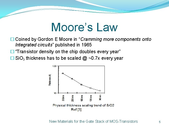
Moore’s Law � Coined by Gordon E Moore in “Cramming more components onto Integrated circuits” published in 1965 � “Transistor density on the chip doubles every year” � Si. O₂ thickness has to be scaled @ ~0. 7 x every year New Materials for the Gate Stack of MOS-Transistors 5

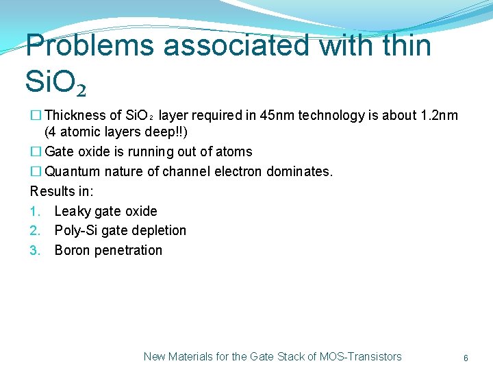
Problems associated with thin Si. O₂ � Thickness of Si. O₂ layer required in 45 nm technology is about 1. 2 nm (4 atomic layers deep!!) � Gate oxide is running out of atoms � Quantum nature of channel electron dominates. Results in: 1. Leaky gate oxide 2. Poly-Si gate depletion 3. Boron penetration New Materials for the Gate Stack of MOS-Transistors 6

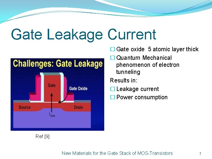
Gate Leakage Current � Gate oxide 5 atomic layer thick � Quantum Mechanical phenomenon of electron tunneling Results in: � Leakage current � Power consumption Ref [9] New Materials for the Gate Stack of MOS-Transistors 7

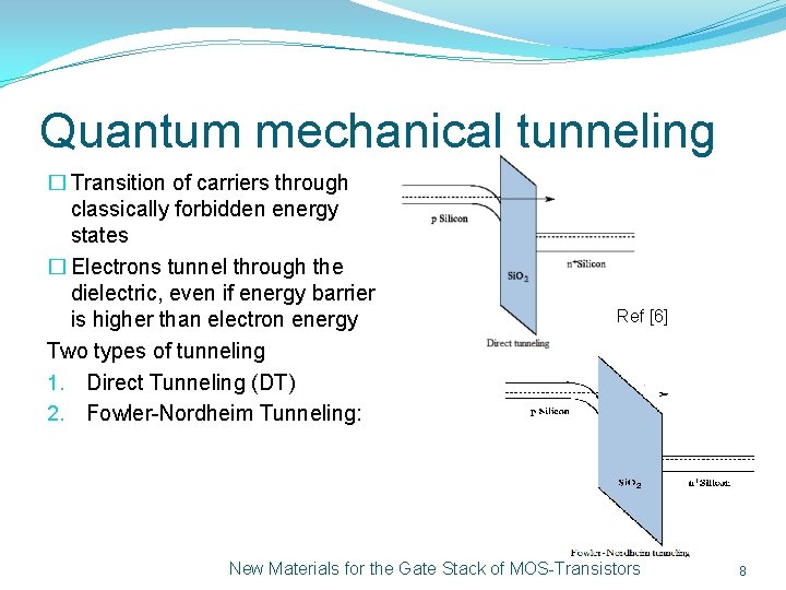
Quantum mechanical tunneling � Transition of carriers through classically forbidden energy states � Electrons tunnel through the dielectric, even if energy barrier is higher than electron energy Two types of tunneling 1. Direct Tunneling (DT) 2. Fowler-Nordheim Tunneling: Ref [6] New Materials for the Gate Stack of MOS-Transistors 8

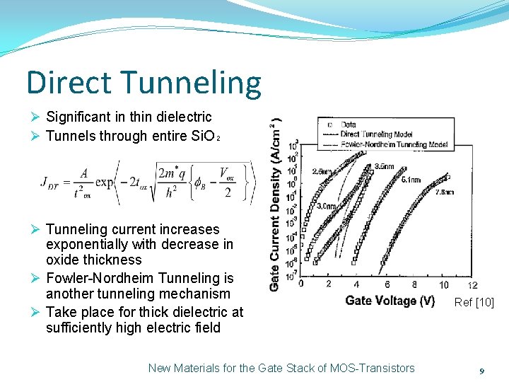
Direct Tunneling Ø Significant in thin dielectric Ø Tunnels through entire Si. O₂ Ø Tunneling current increases exponentially with decrease in oxide thickness Ø Fowler-Nordheim Tunneling is another tunneling mechanism Ø Take place for thick dielectric at sufficiently high electric field New Materials for the Gate Stack of MOS-Transistors Ref [10] 9

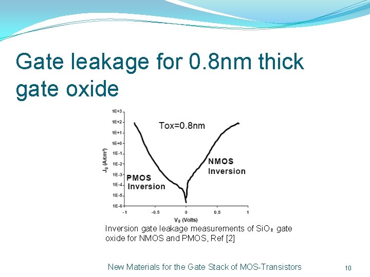
Gate leakage for 0. 8 nm thick gate oxide Inversion gate leakage measurements of Si. O₂ gate oxide for NMOS and PMOS, Ref [2] New Materials for the Gate Stack of MOS-Transistors 10

Consider this. . � Presently a processor chip contains about 100 million transistors � If each transistor leaked a current so high… Heating problems will be ensured… � To reduce leakage, a thicker oxide layer is required. � But this means less control over channel charge Moreover: Ø Gate leakage has direct consequences in PD-SOI MOSFETs Ø Modifies the body voltage and related floating body effects Ø Give rise to “Gate induced floating body effects” (GIFBE) Ø Responsible for kink in characteristics New Materials for the Gate Stack of MOS-Transistors 11

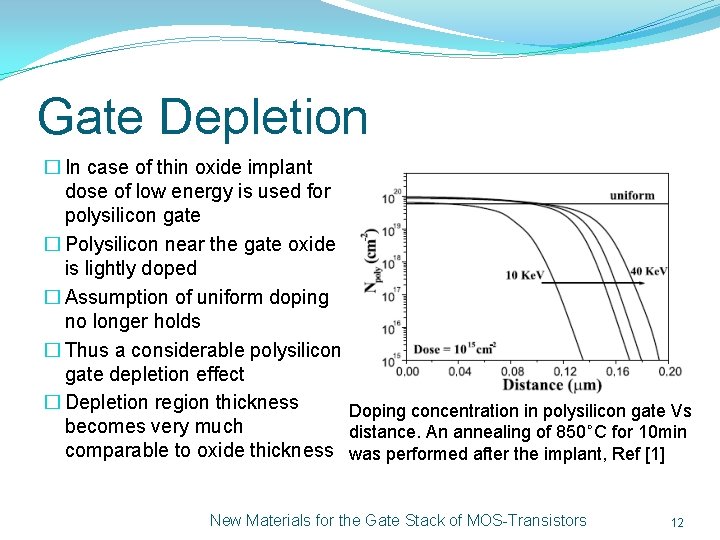
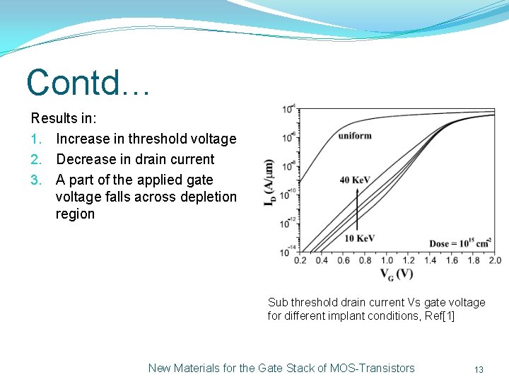
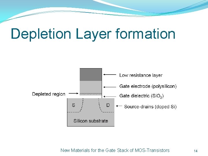
Gate Depletion � In case of thin oxide implant dose of low energy is used for polysilicon gate � Polysilicon near the gate oxide is lightly doped � Assumption of uniform doping no longer holds � Thus a considerable polysilicon gate depletion effect � Depletion region thickness Doping concentration in polysilicon gate Vs becomes very much distance. An annealing of 850˚C for 10 min comparable to oxide thickness was performed after the implant, Ref [1] New Materials for the Gate Stack of MOS-Transistors 12

Contd… Results in: 1. Increase in threshold voltage 2. Decrease in drain current 3. A part of the applied gate voltage falls across depletion region Sub threshold drain current Vs gate voltage for different implant conditions, Ref[1] New Materials for the Gate Stack of MOS-Transistors 13

Depletion Layer formation New Materials for the Gate Stack of MOS-Transistors 14

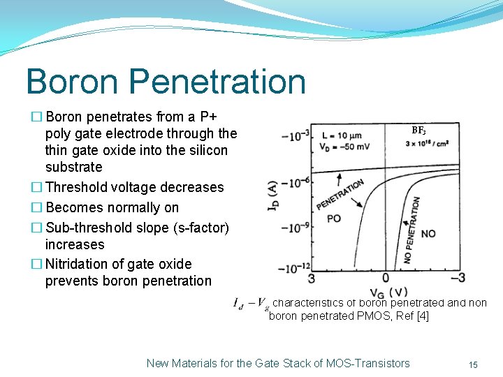
Boron Penetration � Boron penetrates from a P+ poly gate electrode through the thin gate oxide into the silicon substrate � Threshold voltage decreases � Becomes normally on � Sub-threshold slope (s-factor) increases � Nitridation of gate oxide prevents boron penetration BF₃ characteristics of boron penetrated and non boron penetrated PMOS, Ref [4] New Materials for the Gate Stack of MOS-Transistors 15

Key points Nitridation: Ø Performed by RTN Ø Nitrogen concentration should be uniform and small at interface Ø Effective in screening boron penetration down to 2 nm Boron Penetration: Ø Depends significantly on boron dose Ø Extent of boron penetration is judged by s-factor Ø Fluorine enhances boron penetration New Materials for the Gate Stack of MOS-Transistors 16

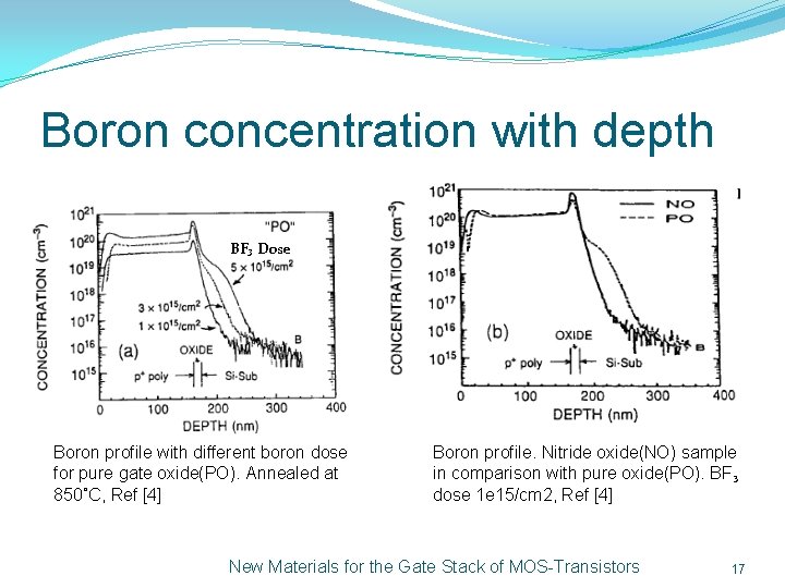
Boron concentration with depth BF₃ Dose Boron profile with different boron dose for pure gate oxide(PO). Annealed at 850˚C, Ref [4] Boron profile. Nitride oxide(NO) sample in comparison with pure oxide(PO). BF₃ dose 1 e 15/cm 2, Ref [4] New Materials for the Gate Stack of MOS-Transistors 17

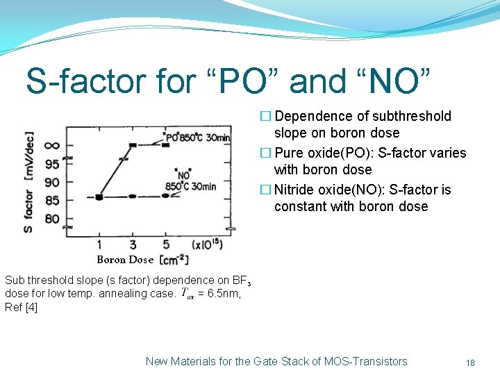
S-factor for “PO” and “NO” � Dependence of subthreshold slope on boron dose � Pure oxide(PO): S-factor varies with boron dose � Nitride oxide(NO): S-factor is constant with boron dose Boron Dose Sub threshold slope (s factor) dependence on BF₃ dose for low temp. annealing case. = 6. 5 nm, Ref [4] New Materials for the Gate Stack of MOS-Transistors 18

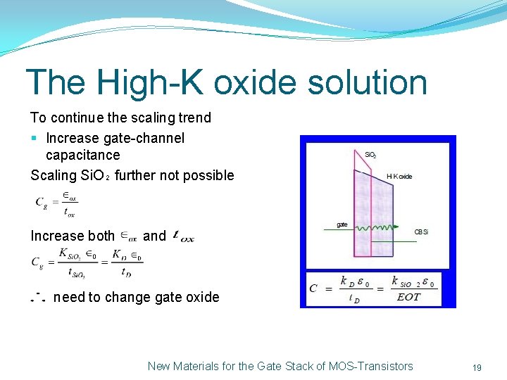
The High-K oxide solution To continue the scaling trend § Increase gate-channel capacitance Scaling Si. O₂ further not possible Increase both and need to change gate oxide New Materials for the Gate Stack of MOS-Transistors 19

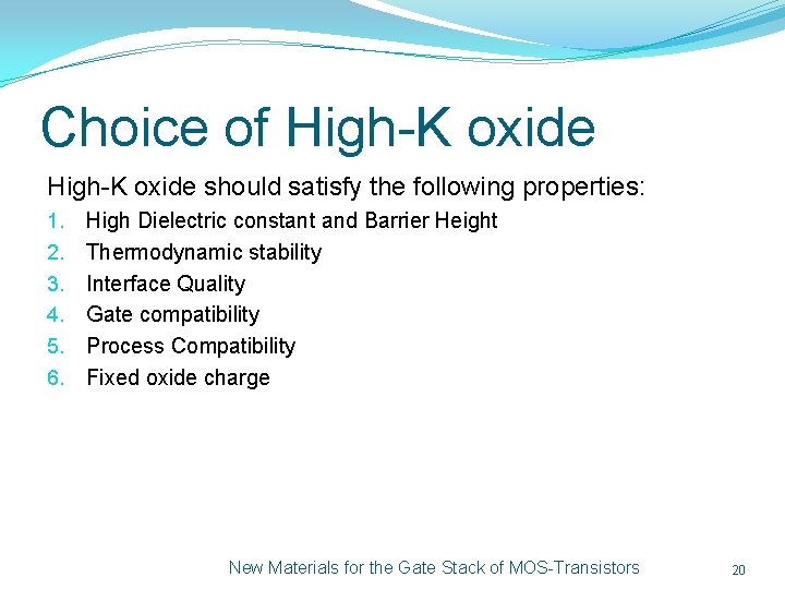
Choice of High-K oxide should satisfy the following properties: 1. 2. 3. 4. 5. 6. High Dielectric constant and Barrier Height Thermodynamic stability Interface Quality Gate compatibility Process Compatibility Fixed oxide charge New Materials for the Gate Stack of MOS-Transistors 20
![Potential HighK materials Ref 5 Which one of them is appropriate Dielectric constant Potential High-K materials Ref [5] Which one of them is appropriate? ? Dielectric constant](https://slidetodoc.com/presentation_image_h2/5cbe625a5326c336cf7538444fb5b5df/image-21.jpg)
Potential High-K materials Ref [5] Which one of them is appropriate? ? Dielectric constant and band gap of a given material generally exhibit an inverse relationship? ? (some materials have significant departure from this trend) New Materials for the Gate Stack of MOS-Transistors 21

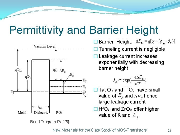
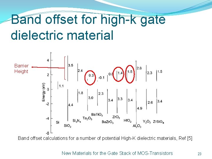
Permittivity and Barrier Height � Barrier Height: � Tunneling current is negligible � Leakage current increases exponentially with decreasing barrier height � Ta₂O₅ and Ti. O₂ have small value of and hence large leakage current � Hf. O₂ and Zr. O₂ offer higher value of K and Band Diagram Ref [5] New Materials for the Gate Stack of MOS-Transistors 22

Band offset for high-k gate dielectric material Barrier Height Band offset calculations for a number of potential High-K dielectric materials, Ref [5] New Materials for the Gate Stack of MOS-Transistors 23

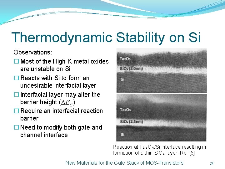
Thermodynamic Stability on Si Observations: � Most of the High-K metal oxides are unstable on Si � Reacts with Si to form an undesirable interfacial layer � Interfacial layer may alter the barrier height ( ) � Require an interfacial reaction barrier � Need to modify both gate and channel interface Reaction at Ta₂O₅/Si interface resulting in formation of a thin Si. O₂ layer, Ref [5] New Materials for the Gate Stack of MOS-Transistors 24

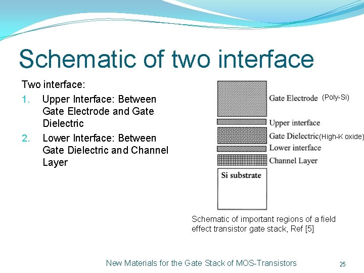
Schematic of two interface Two interface: 1. Upper Interface: Between Gate Electrode and Gate Dielectric 2. Lower Interface: Between Gate Dielectric and Channel Layer (Poly-Si) (High-K oxide) Schematic of important regions of a field effect transistor gate stack, Ref [5] New Materials for the Gate Stack of MOS-Transistors 25

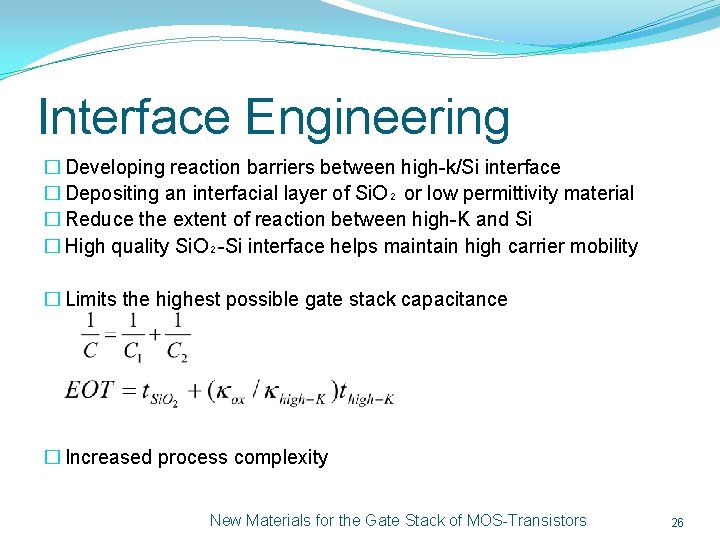
Interface Engineering � Developing reaction barriers between high-k/Si interface � Depositing an interfacial layer of Si. O₂ or low permittivity material � Reduce the extent of reaction between high-K and Si � High quality Si. O₂-Si interface helps maintain high carrier mobility � Limits the highest possible gate stack capacitance � Increased process complexity New Materials for the Gate Stack of MOS-Transistors 26

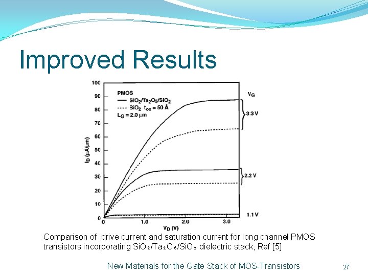
Improved Results Comparison of drive current and saturation current for long channel PMOS transistors incorporating Si. O₂/Ta₂O₅/Si. O₂ dielectric stack, Ref [5] New Materials for the Gate Stack of MOS-Transistors 27

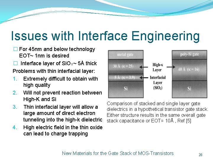
Issues with Interface Engineering � For 45 nm and below technology EOT~ 1 nm is desired � Interface layer of Si. O₂~ 5Å thick Problems with thin interfacial layer: 1. Extremely difficult to obtain with high quality 2. Will not prevent reaction between High-K and Si 3. Thin interfacial layer will allow a large amount of direct electron tunneling into the high-k dielectric 4. High electric field in the thin oxide can lead to charge trapping Comparison of stacked and single layer gate dielectrics in a hypothetical transistor gate stack. Either structure results in the same overall gate stack capacitance or EOT= 10Å , Ref [5] New Materials for the Gate Stack of MOS-Transistors 28

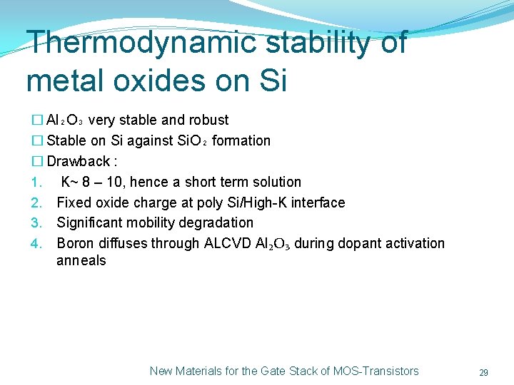
Thermodynamic stability of metal oxides on Si � Al₂O₃ very stable and robust � Stable on Si against Si. O₂ formation � Drawback : 1. K~ 8 – 10, hence a short term solution 2. Fixed oxide charge at poly Si/High-K interface 3. Significant mobility degradation 4. Boron diffuses through ALCVD Al₂O₃ during dopant activation anneals New Materials for the Gate Stack of MOS-Transistors 29

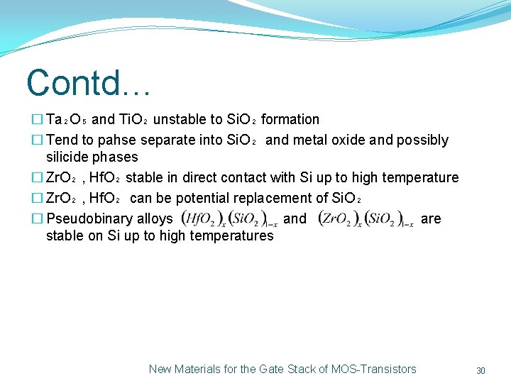
Contd… � Ta₂O₅ and Ti. O₂ unstable to Si. O₂ formation � Tend to pahse separate into Si. O₂ and metal oxide and possibly silicide phases � Zr. O₂ , Hf. O₂ stable in direct contact with Si up to high temperature � Zr. O₂ , Hf. O₂ can be potential replacement of Si. O₂ � Pseudobinary alloys and are stable on Si up to high temperatures New Materials for the Gate Stack of MOS-Transistors 30

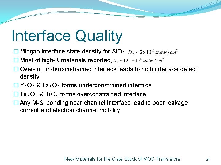
Interface Quality � Midgap interface state density for Si. O₂ , � Most of high-K materials reported, � Over- or underconstrained interface leads to high interface defect density � Y₂O₃ & La₂O₃ forms underconstrained interface � Ta₂O₅ & Ti. O₂ forms overconstrained interface � Any M-Si bonding near channel interface lead to poor leakage current and electron channel mobility New Materials for the Gate Stack of MOS-Transistors 31

Contd…. � Zr. O₂ , Hf. O₂ have high oxygen diffusivities � Any annealing step with excess oxygen will lead to diffusion of oxygen and result in formation of Si. O₂ at high-K/Si interface � Severely compromise the capacitance gain New Materials for the Gate Stack of MOS-Transistors 32

Film Morphology Polycrystalline films: Amorphous films: Ø Grain boundaries serve as highleakage paths, and this may lead to the need for an amorphous interfacial layer to reduce leakage current Ø Grain size and orientation changes throughout the film causing variations in K Ø Hence are problematic Ø Exhibit isotropic electrical properties Ø Don’t suffer from grain boundaries Ø Can easily be deposited An amorphous film structure is the ideal one New Materials for the Gate Stack of MOS-Transistors 33

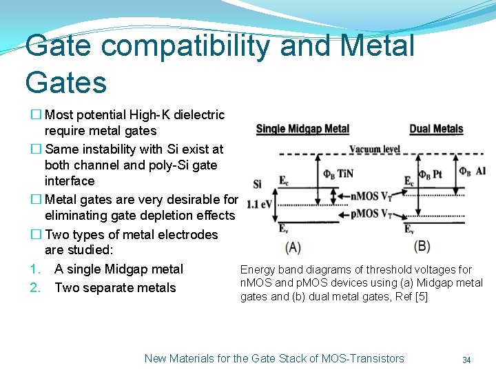
Gate compatibility and Metal Gates � Most potential High-K dielectric require metal gates � Same instability with Si exist at both channel and poly-Si gate interface � Metal gates are very desirable for eliminating gate depletion effects � Two types of metal electrodes are studied: 1. A single Midgap metal Energy band diagrams of threshold voltages for n. MOS and p. MOS devices using (a) Midgap metal 2. Two separate metals gates and (b) dual metal gates, Ref [5] New Materials for the Gate Stack of MOS-Transistors 34

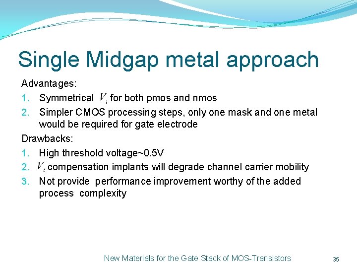
Single Midgap metal approach Advantages: 1. Symmetrical for both pmos and nmos 2. Simpler CMOS processing steps, only one mask and one metal would be required for gate electrode Drawbacks: 1. High threshold voltage~0. 5 V 2. compensation implants will degrade channel carrier mobility 3. Not provide performance improvement worthy of the added process complexity New Materials for the Gate Stack of MOS-Transistors 35

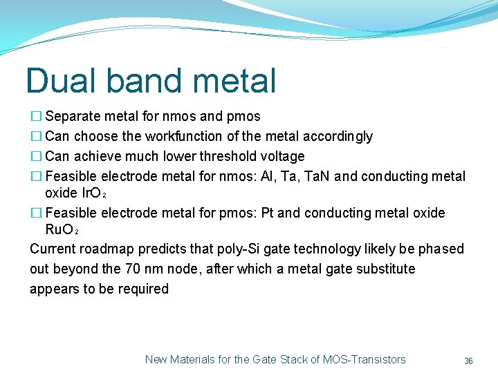
Dual band metal � Separate metal for nmos and pmos � Can choose the workfunction of the metal accordingly � Can achieve much lower threshold voltage � Feasible electrode metal for nmos: Al, Ta. N and conducting metal oxide Ir. O₂ � Feasible electrode metal for pmos: Pt and conducting metal oxide Ru. O₂ Current roadmap predicts that poly-Si gate technology likely be phased out beyond the 70 nm node, after which a metal gate substitute appears to be required New Materials for the Gate Stack of MOS-Transistors 36

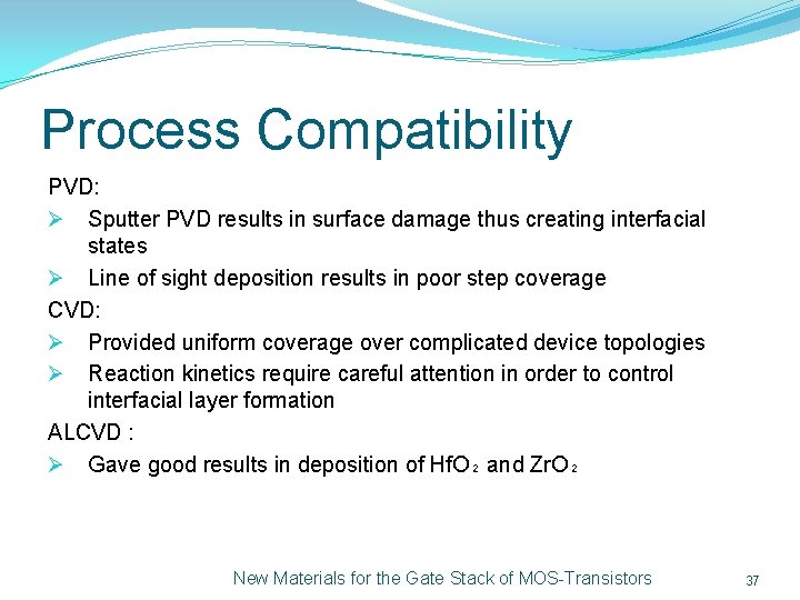
Process Compatibility PVD: Ø Sputter PVD results in surface damage thus creating interfacial states Ø Line of sight deposition results in poor step coverage CVD: Ø Provided uniform coverage over complicated device topologies Ø Reaction kinetics require careful attention in order to control interfacial layer formation ALCVD : Ø Gave good results in deposition of Hf. O₂ and Zr. O₂ New Materials for the Gate Stack of MOS-Transistors 37

Replacing poly-Si/Si. O₂ by poly-Si/High-K Transistors built using Poly-Si gate and High-K gate oxide suffers from: 1. High threshold voltage because of Fermi level pinning at poly. Si/High-K interface 2. Degraded channel carrier mobility New Materials for the Gate Stack of MOS-Transistors 38

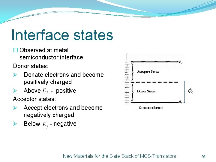
Interface states � Observed at metal semiconductor interface Donor states: Ø Donate electrons and become positively charged Ø Above - positive Acceptor states: Ø Accept electrons and become negatively charged Ø Below - negative Acceptor States Donor States Semiconductor New Materials for the Gate Stack of MOS-Transistors 39

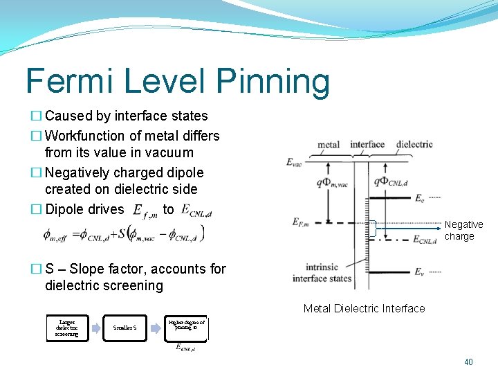
Fermi Level Pinning � Caused by interface states � Workfunction of metal differs from its value in vacuum � Negatively charged dipole created on dielectric side � Dipole drives to Negative charge � S – Slope factor, accounts for dielectric screening Metal Dielectric Interface Larger dielectric screening Smaller S Higher degree of pinning to 40

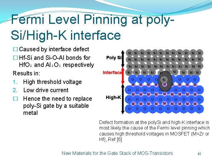
Fermi Level Pinning at poly. Si/High-K interface � Caused by interface defect � Hf-Si and Si-O-Al bonds for Hf. O₂ and Al₂O₃ respectively Results in: 1. High threshold voltage 2. Low drive current � Hence the need to replace poly-Si gate by a suitable metal Defect formation at the poly. Si and high-K interface is most likely the cause of the Fermi level pinning which causes high threshold voltages in MOSFET (M=Zr or Hf), Ref [6] New Materials for the Gate Stack of MOS-Transistors 41

Mobility Degradation Reason for mobility degradation: Ø Surface phonon scattering in high-κ dielectrics Mechanism: 1. High-K dielectric has polarizable metal oxygen bonds 2. Oscillating dipoles interacts with channel carriers when gate plasma oscillations and phonons in high-K are in resonance 3. This resonance condition leads to significant degradation of channel carrier mobility Resonance occurs when gate carrier density is To Avoid: Ø Use metal whose free carrier density exceeds Ø Resonance condition is not satisfied Ø Weakens the interaction New Materials for the Gate Stack of MOS-Transistors 42
![Surface Phonon Limited Mobility Ref 7 Ref 8 New Materials for the Gate Stack Surface Phonon Limited Mobility Ref [7] Ref [8] New Materials for the Gate Stack](https://slidetodoc.com/presentation_image_h2/5cbe625a5326c336cf7538444fb5b5df/image-43.jpg)
Surface Phonon Limited Mobility Ref [7] Ref [8] New Materials for the Gate Stack of MOS-Transistors 43

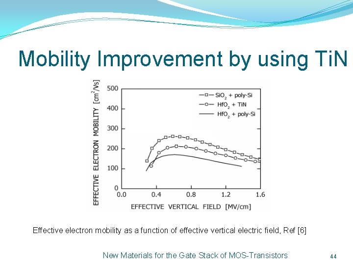
Mobility Improvement by using Ti. N Effective electron mobility as a function of effective vertical electric field, Ref [6] New Materials for the Gate Stack of MOS-Transistors 44

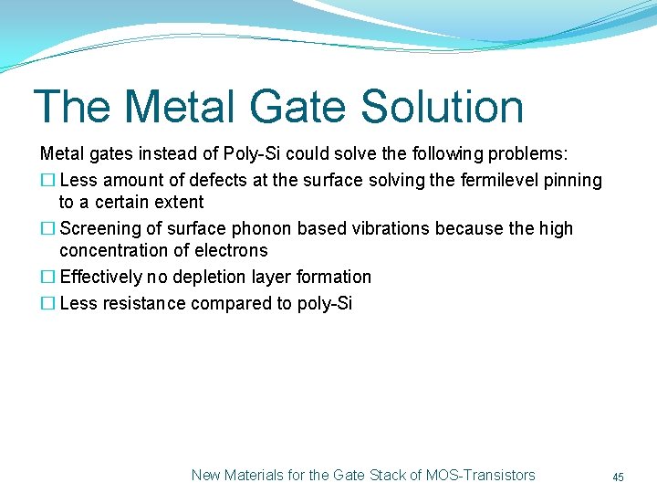
The Metal Gate Solution Metal gates instead of Poly-Si could solve the following problems: � Less amount of defects at the surface solving the fermilevel pinning to a certain extent � Screening of surface phonon based vibrations because the high concentration of electrons � Effectively no depletion layer formation � Less resistance compared to poly-Si New Materials for the Gate Stack of MOS-Transistors 45

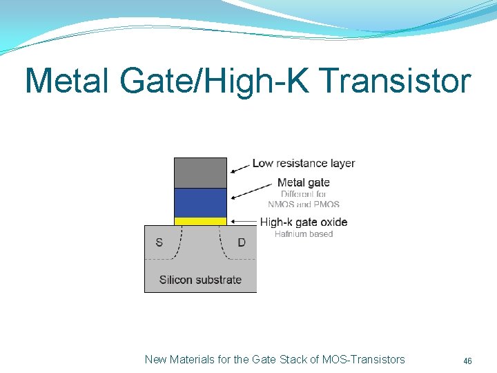
Metal Gate/High-K Transistor New Materials for the Gate Stack of MOS-Transistors 46

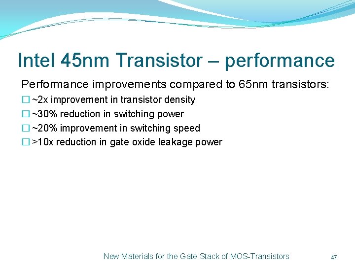
Intel 45 nm Transistor – performance Performance improvements compared to 65 nm transistors: � ~2 x improvement in transistor density � ~30% reduction in switching power � ~20% improvement in switching speed � >10 x reduction in gate oxide leakage power New Materials for the Gate Stack of MOS-Transistors 47

Summary 1. 2. 3. 4. 5. Problems associated with thin Si. O₂ need to be replaced by High-K oxide for 45 nm and below technology Hf. O₂ and Zr. O₂ show promising results Problems associated with poly-Si/High-K interface Use of metal gate instead of poly-Si give better results New Materials for the Gate Stack of MOS-Transistors 48
![References 1 R Shireen et al Influence of polysilicongate depletion on the subthreshold References [1] R. Shireen, et al. , "Influence of polysilicon-gate depletion on the subthreshold](https://slidetodoc.com/presentation_image_h2/5cbe625a5326c336cf7538444fb5b5df/image-49.jpg)
References [1] R. Shireen, et al. , "Influence of polysilicon-gate depletion on the subthreshold behaviour of submicron MOSFETs", December 2010 [online] [2] R. Chau, S. Datta, M. Doczy, J. Kavalieros, and M. Metz, “Gate dielectric scaling for high performance CMOS: from Si. O 2 to high-κ”, Extended Abstract of International Workshop on Gate Insulator, Tokyo, Japan, pp. 124– 126, 2003 [3] K. Mistry, et al. , “A 45 nm Logic Technology with High-k+Metal Gate Transistors, Strained Silicon, 9 Cu Interconnect Layers, 193 nm Dry Patterning, and 100% Pb-free Packaging” in Electron Devices Meeting, 2007. IEDM 2007. IEEE International, January 2008, pp. 247 -250 [4] T. Morimoto, et al. , "Effects of boron penetration and resultant limitations in ultra thin pure-oxide and nitrided-oxide gate-films" in Electron Devices Meeting, 1990. IEDM '90. Technical Digest. , International, pp. 429 -432 [5] G. Wilk, et al. , "High-k gate dielectrics: Current status and materials properties considerations", Applied Physics Journal, January 2001 New Materials for the Gate Stack of MOS-Transistors 49
![References 6 R Chau et al Advanced metal gatehigh dielectric stacks for high References [6] R. Chau et al. , “Advanced metal gate/high-_ dielectric stacks for high](https://slidetodoc.com/presentation_image_h2/5cbe625a5326c336cf7538444fb5b5df/image-50.jpg)
References [6] R. Chau et al. , “Advanced metal gate/high-_ dielectric stacks for high performance CMOS transistors”, in AVS 5 th Int. Microelectronics Interfaces Conf. , Santa Clara, CA, 2004, pp. 3– 5. [7] R. Chau, et al. , “Application of high-κ gate dielectrics and metal gate electrodes to enable silicon and non-silicon logic nanotechnology, ” Microelectron. Eng. , vol. 80, pp. 1 – 6, Jun. 2005 [8] M. T. Bohr, R. Chau, T. Ghani and K. Mistry, “The high-k solution”, IEEE Spectrum-the high-k solution, October 2007 [9]http: //www. xtremesystems. org/forums/showthread. php? t=253738&page=4[ Accessed: 3 rd December. 2010] [10] Chenming Hu, “Gate Oxide Scaling Limits and Projection”, in Electron Devices Meeting, 1996. IEDM 1996 , pp. 319 -322 [11] http: //www. iue. tuwien. ac. at/phd/entner/node 23. html [Accessed: 6 th December, 2010] New Materials for the Gate Stack of MOS-Transistors 50

THANK YOU!! New Materials for the Gate Stack of MOS-Transistors 51