
New era for Materials Technology in Korea PRICM8
- Slides: 51
New era for Materials Technology in Korea PRICM-8 Waikoloa, Hawaii August 5, 2013 Dr. Dongwha Kum Acting Vice President, NAEK Endowed Chair Researcher, KIST
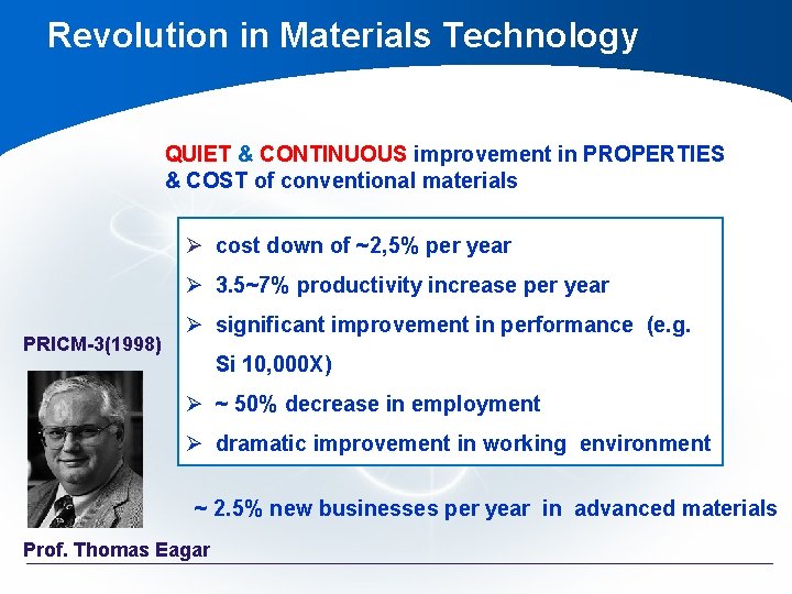
Revolution in Materials Technology QUIET & CONTINUOUS improvement in PROPERTIES & COST of conventional materials Ø cost down of ~2, 5% per year Ø 3. 5~7% productivity increase per year PRICM-3(1998) Ø significant improvement in performance (e. g. Si 10, 000 X) Ø ~ 50% decrease in employment Ø dramatic improvement in working environment ~ 2. 5% new businesses per year in advanced materials Prof. Thomas Eagar
Contents 1 Introduction 2 Matured New Materials 3 Challenge Forwards 4 Summary & Conclusion
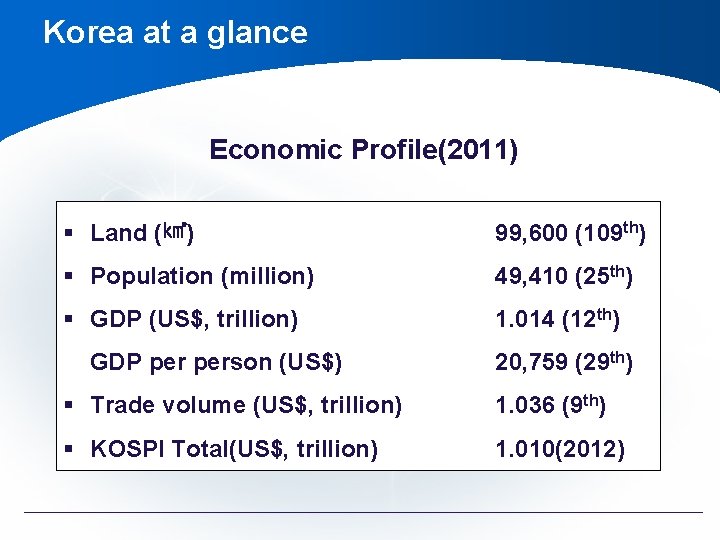
Korea at a glance Economic Profile(2011) § Land (㎢) 99, 600 (109 th) § Population (million) 49, 410 (25 th) § GDP (US$, trillion) 1. 014 (12 th) GDP person (US$) 20, 759 (29 th) § Trade volume (US$, trillion) 1. 036 (9 th) § KOSPI Total(US$, trillion) 1. 010(2012)
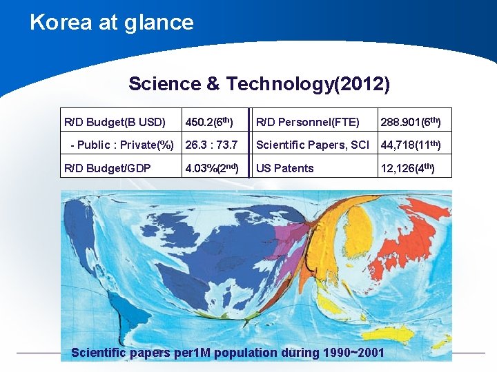
Korea at glance Science & Technology(2012) R/D Budget(B USD) 450. 2(6 th) R/D Personnel(FTE) 288. 901(6 th) - Public : Private(%) 26. 3 : 73. 7 Scientific Papers, SCI 44, 718(11 th) R/D Budget/GDP 4. 03%(2 nd) US Patents 12, 126(4 th) Scientific papers per 1 M population during 1990~2001
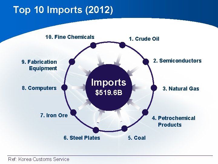
Top 10 Imports (2012) 10. Fine Chemicals 1. Crude Oil 2. Semiconductors 9. Fabrication Equipment Imports 8. Computers 3. Natural Gas $519. 6 B 7. Iron Ore 6. Steel Plates Ref: Korea Customs Service 4. Petrochemical Products 5. Coal
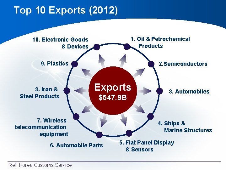
Top 10 Exports (2012) 1. Oil & Petrochemical Products 10. Electronic Goods & Devices 9. Plastics 8. Iron & Steel Products 2. Semiconductors Exports $547. 9 B 7. Wireless telecommunication equipment 6. Automobile Parts Ref: Korea Customs Service 3. Automobiles 4. Ships & Marine Structures 5. Flat Panel Display & Sensors
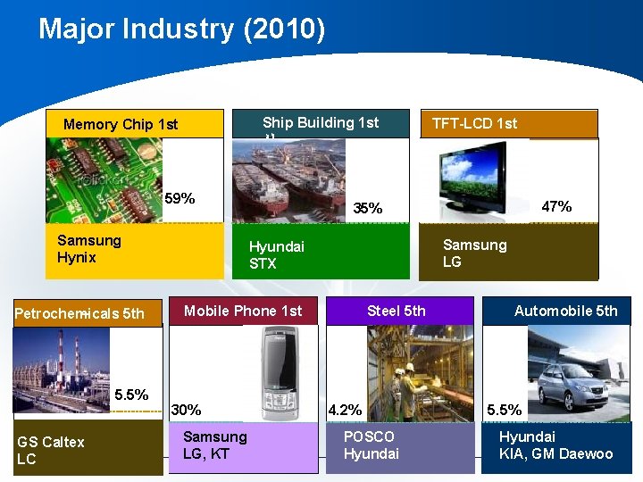
Major Industry (2010) Ship Building 1 st 선 Memory Chip 1 st 59% 49. 3% Samsung Hynix – Petrochemicals 5 th 5. 5% 30. 2% GS Caltex LC Samsung LG Mobile Phone 1 st Samsung LG, KT 47% 30. 2% 35% 32. 4% Hyundai STX 30% 25. 3% TFT-LCD 1 st Steel 5 th 4. 2% 3. 9% POSCO Hyundai Automobile 5 th 5. 5% Hyundai KIA, GM Daewoo
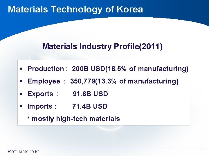
Materials Technology of Korea Materials Industry Profile(2011) § Production : 200 B USD(18. 5% of manufacturing) § Employee : 350, 779(13. 3% of manufacturing) § Exports : 91. 6 B USD § Imports : 71. 4 B USD * mostly high-tech materials Ref: : kims. re. kr
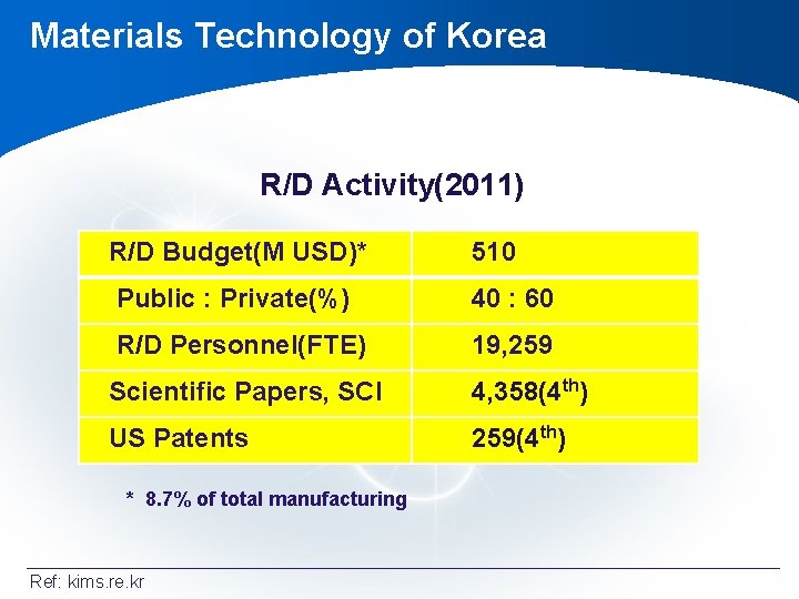
Materials Technology of Korea R/D Activity(2011) R/D Budget(M USD)* 510 Public : Private(%) 40 : 60 R/D Personnel(FTE) 19, 259 Scientific Papers, SCI 4, 358(4 th) US Patents 259(4 th) * 8. 7% of total manufacturing Ref: kims. re. kr
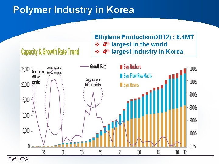
Polymer Industry in Korea Ethylene Production(2012) : 8. 4 MT v 4 th largest in the world v 4 th largest industry in Korea Ref: KPA
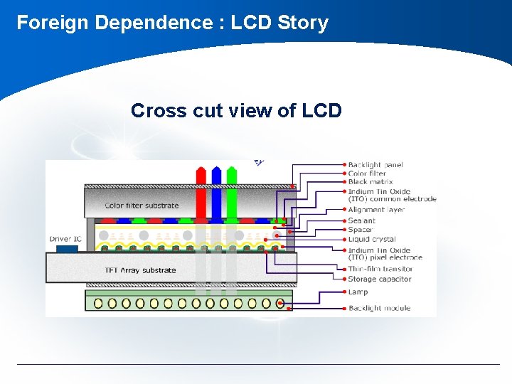
Foreign Dependence : LCD Story Cross cut view of LCD
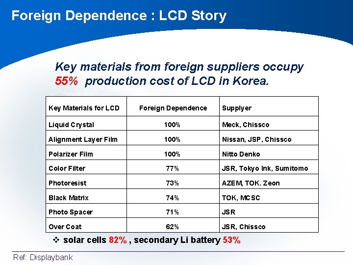
Foreign Dependence : LCD Story Key materials from foreign suppliers occupy 55% production cost of LCD in Korea. Key Materials for LCD Foreign Dependence Supplyer Liquid Crystal 100% Meck, Chissco Alignment Layer Film 100% Nissan, JSP, Chissco Polarizer Film 100% Nitto Denko Color Filter 77% JSR, Tokyo Ink, Sumitomo Photoresist 73% AZEM, TOK. Zeon Black Matrix 74% TOK, MCSC Photo Spacer 71% JSR Over Coat 62% JSR, Chissco v solar cells 82% , secondary Li battery 53% Ref: Displaybank
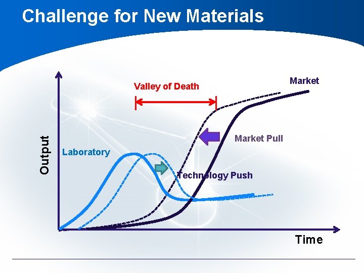
Challenge for New Materials Market Output Valley of Death Market Pull Laboratory Technology Push Time
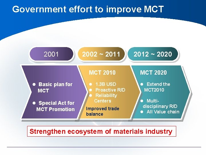
Government effort to improve MCT 2001 l Basic plan for MCT l Special Act for MCT Promotion 2002 ~ 2011 2012 ~ 2020 MCT 2010 MCT 2020 l 1. 3 B USD l Proactive R/D l Reliability Centers l Extend the MCT 2010 Improved trade balance l Multi disciplinary R/D l All Value chain Strengthen ecosystem of materials industry
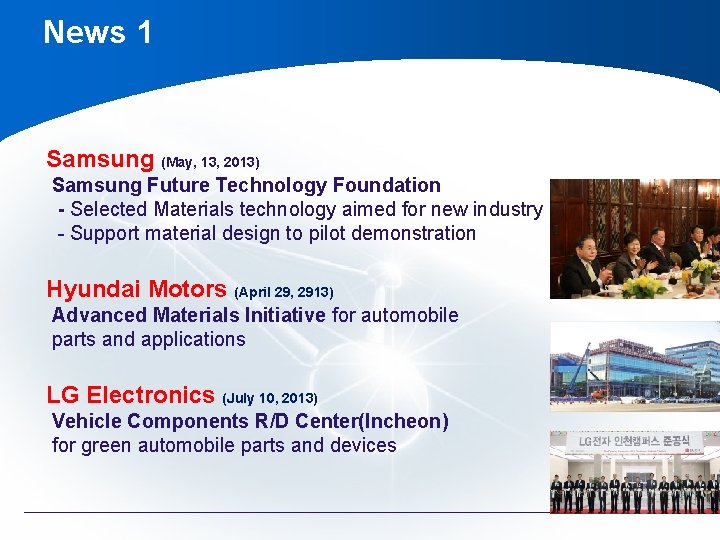
News 1 Samsung (May, 13, 2013) Samsung Future Technology Foundation - Selected Materials technology aimed for new industry - Support material design to pilot demonstration Hyundai Motors (April 29, 2913) Advanced Materials Initiative for automobile parts and applications LG Electronics (July 10, 2013) Vehicle Components R/D Center(Incheon) for green automobile parts and devices
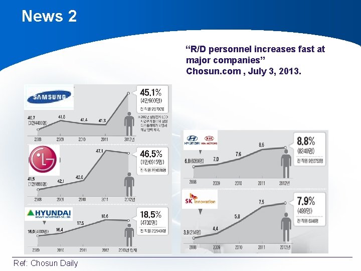
News 2 “R/D personnel increases fast at major companies” Chosun. com , July 3, 2013. Ref: Chosun Daily
Contents 1 Introduction 2 Matured New Materials 3 Challenge Forwards 4 Summary & Conclusion
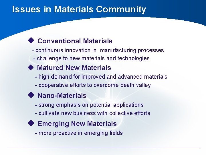
Issues in Materials Community u Conventional Materials - continuous innovation in manufacturing processes - challenge to new materials and technologies u Matured New Materials - high demand for improved and advanced materials - cooperative efforts to overcome death valley u Nano-Materials - strong emphasis on potential applications - cultivate new business with collective efforts u Emerging New Materials - more proactive in emerging fields
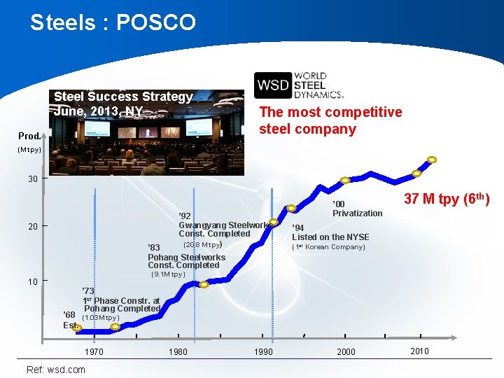
Steels : POSCO Steel Success Strategy June, 2013, NY Prod. The most competitive steel company (M tpy) 30 ’ 92 Gwangyang Steelworks Const. Completed (20. 8 M tpy) 20 ’ 83 Pohang Steelworks Const. Completed ’ 00 Privatization 37 M tpy (6 th) ’ 94 Listed on the NYSE (1 st Korean Company) (9. 1 M tpy) 10 ’ 73 1 st Phase Constr. at Pohang Completed ’ 68 (1. 03 M tpy) Est. 1970 Ref: wsd. com 1980 1990 2000 2010
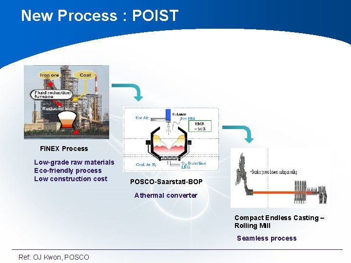
New Process : POIST FINEX Process Low-grade raw materials Eco-friendly process Low construction cost POSCO-Saarstatl-BOP Athermal converter Compact Endless Casting – Rolling Mill Seamless process Ref: OJ Kwon, POSCO
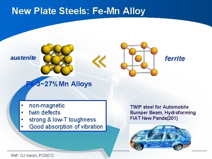
New Plate Steels: Fe-Mn Alloy austenite « ferrite Fe-3~27%Mn Alloys • • non-magnetic twin defects strong & low-T toughness Good absorption of vibration Ref: OJ Kwon, POSCO TWIP steel for Automobile Bumper Beam, Hydroforming FIAT New Panda(201)
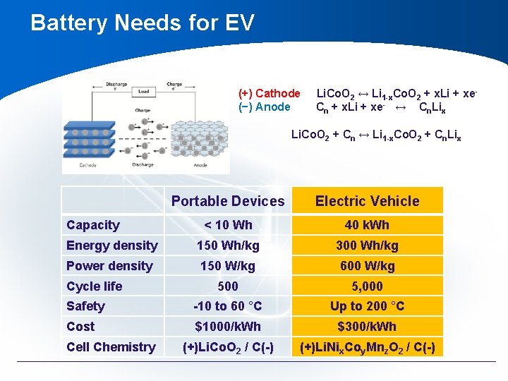
Battery Needs for EV (+) Cathode Li. Co. O 2 ↔ Li 1 -x. Co. O 2 + x. Li + xe(−) Anode Cn + x. Li + xe- ↔ Cn. Lix Li. Co. O 2 + Cn ↔ Li 1 -x. Co. O 2 + Cn. Lix Portable Devices Electric Vehicle < 10 Wh 40 k. Wh Energy density 150 Wh/kg 300 Wh/kg Power density 150 W/kg 600 W/kg 500 5, 000 Safety -10 to 60 °C Up to 200 °C Cost $1000/k. Wh $300/k. Wh (+)Li. Co. O 2 / C(-) (+)Li. Nix. Coy. Mnz. O 2 / C(-) Capacity Cycle life Cell Chemistry
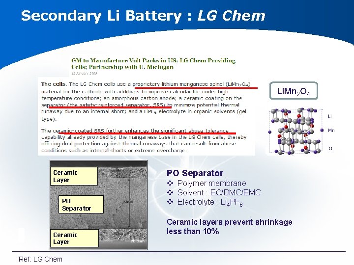
Secondary Li Battery : LG Chem Li. Mn 2 O 4 Ceramic Layer PO Separator Ceramic Layer Ref: LG Chem PO Separator v Polymer membrane v Solvent : EC/DMC/EMC v Electrolyte : Li 4 PF 6 Ceramic layers prevent shrinkage less than 10%
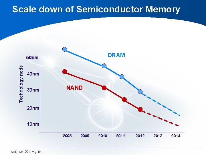
Scale down of Semiconductor Memory DRAM Technology node 50 nm 40 nm 30 nm NAND 20 nm 10 nm 2008 source: SK Hynix 2009 2010 2011 2012 2013 2014
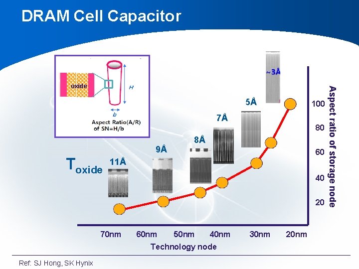
DRAM Cell Capacitor 5Å 100 7Å 80 9Å Toxide 8Å 60 11Å 40 20 70 nm 60 nm 50 nm 40 nm Technology node Ref: SJ Hong, SK Hynix 30 nm 20 nm Aspect ratio of storage node oxide
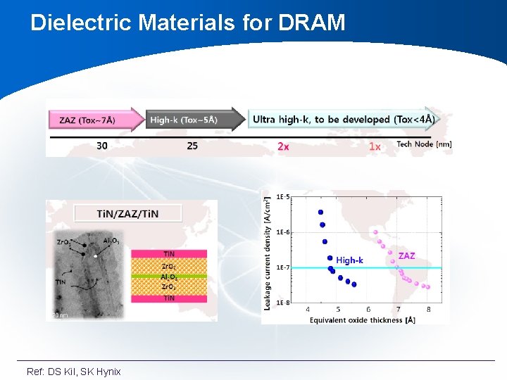
Dielectric Materials for DRAM Ref: DS Kil, SK Hynix
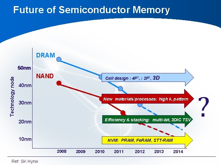
Future of Semiconductor Memory DRAM Technology node 50 nm NAND Cell design : 4 F 2, : 2 F 2, 3 D 40 nm New materials/processes: high k, pattern 30 nm Efficiency & stacking: multi-bit, 3 DIC TSV 20 nm 10 nm NVM: PRAM, Fe. RAM, STT-RAM 2008 Ref: SK Hynix 2009 2010 2011 2012 2013 2014
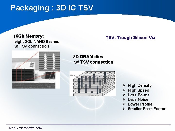
Packaging : 3 D IC TSV 16 Gb Memory: eight 2 Gb NAND flashes TSV: Trough Silicon Via w/ TSV connection 3 D DRAM dies w/ TSV connection Ø Ø Ø Ref: i-micronews. com High Density High Speed Less Power Less Noise Lower Profile Smaller Form Factor
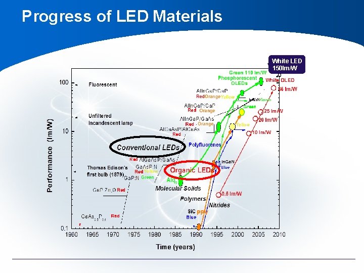
Progress of LED Materials White LED 150 lm/W
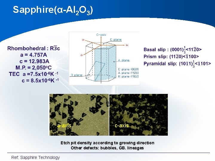
Sapphire(α-Al 2 O 3) a-axis c-axis Etch pit density according to growing direction Other defects: bubbles, GB. lineages Ref: Sapphire Technology
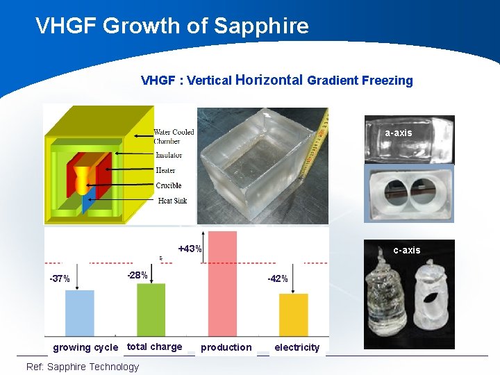
VHGF Growth of Sapphire VHGF : Vertical Horizontal Gradient Freezing a-axis +43% -37% -28% growing cycle total charge Ref: Sapphire Technology c-axis -42% production electricity
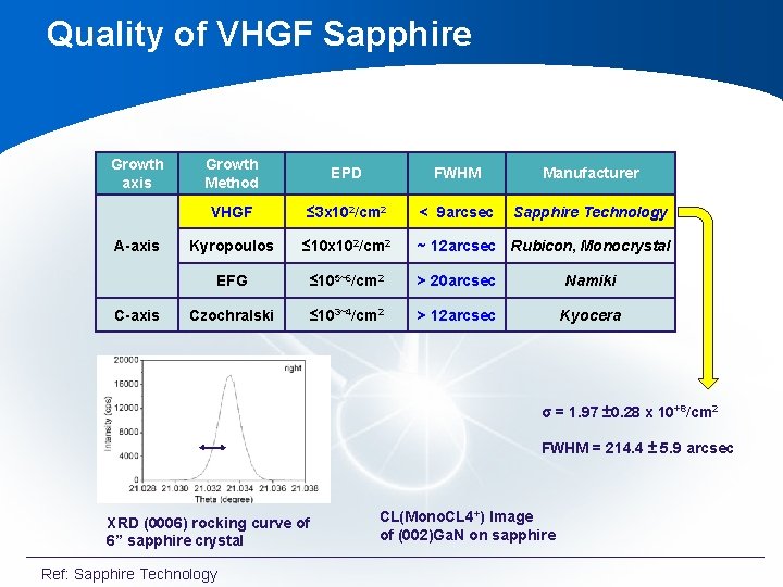
Quality of VHGF Sapphire Growth axis A-axis C-axis Growth Method EPD FWHM Manufacturer VHGF ≤ 3 x 10²/cm 2 < 9 arcsec Sapphire Technology Kyropoulos ≤ 10 x 102/cm 2 ~ 12 arcsec Rubicon, Monocrystal EFG ≤ 105~6/cm 2 > 20 arcsec Namiki Czochralski ≤ 103~4/cm 2 > 12 arcsec Kyocera σ = 1. 97 ± 0. 28 x 10+8/cm 2 FWHM = 214. 4 ± 5. 9 arcsec XRD (0006) rocking curve of 6” sapphire crystal Ref: Sapphire Technology CL(Mono. CL 4+) Image of (002)Ga. N on sapphire
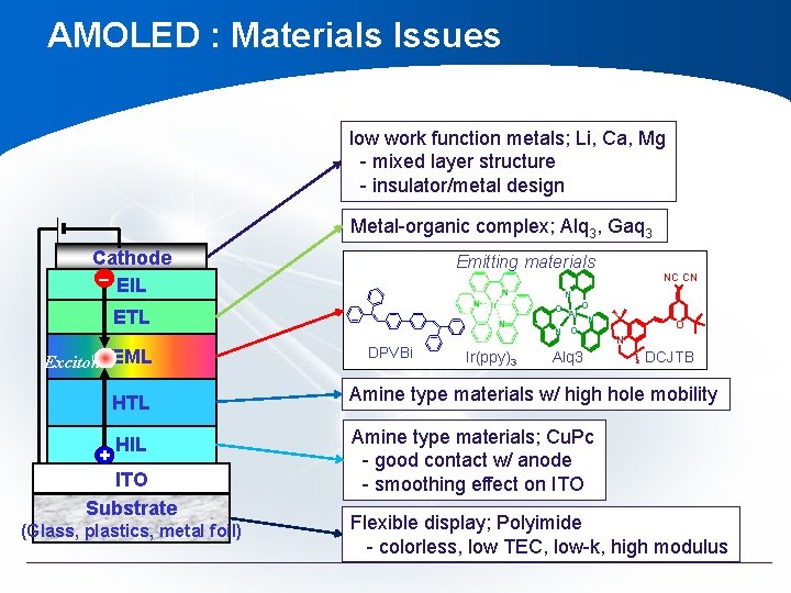
AMOLED : Materials Issues low work function metals; Li, Ca, Mg - mixed layer structure - insulator/metal design Metal-organic complex; Alq 3, Gaq 3 Cathode - EIL Emitting materials O ETL Exciton EML + NC CN N Al N O DPVBi Ir(ppy)3 O N Alq 3 O N DCJTB HTL Amine type materials w/ high hole mobility HIL Amine type materials; Cu. Pc - good contact w/ anode - smoothing effect on ITO Substrate (Glass, plastics, metal foil) Flexible display; Polyimide - colorless, low TEC, low-k, high modulus
1 Introduction 2 Matured New Materials 3 Challenge Forwards 4 Summary & Conclusion
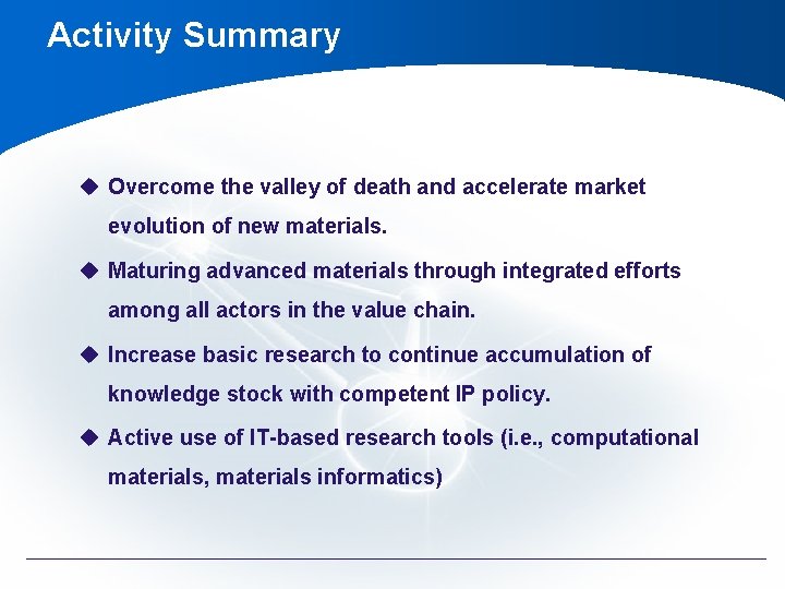
Activity Summary u Overcome the valley of death and accelerate market evolution of new materials. u Maturing advanced materials through integrated efforts among all actors in the value chain. u Increase basic research to continue accumulation of knowledge stock with competent IP policy. u Active use of IT-based research tools (i. e. , computational materials, materials informatics)
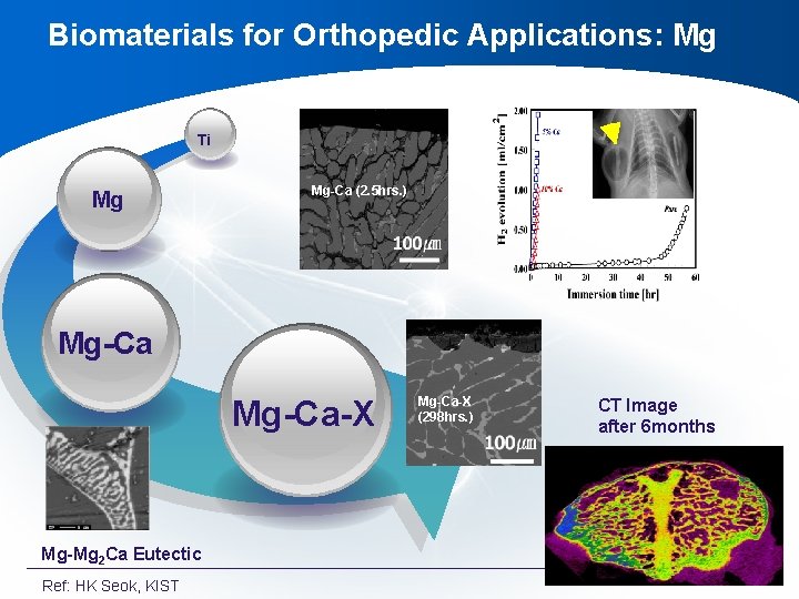
Biomaterials for Orthopedic Applications: Mg Ti Mg Mg-Ca (2. 5 hrs. ) Mg-Ca-X Mg-Mg 2 Ca Eutectic Ref: HK Seok, KIST Mg-Ca-X (298 hrs. ) CT Image after 6 months
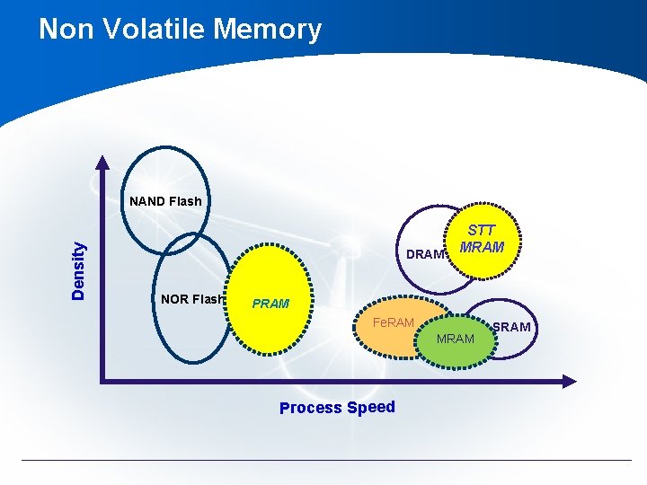
Non Volatile Memory Density NAND Flash DRAM NOR Flash STT MRAM PRAM Fe. RAM MRAM Process Speed SRAM
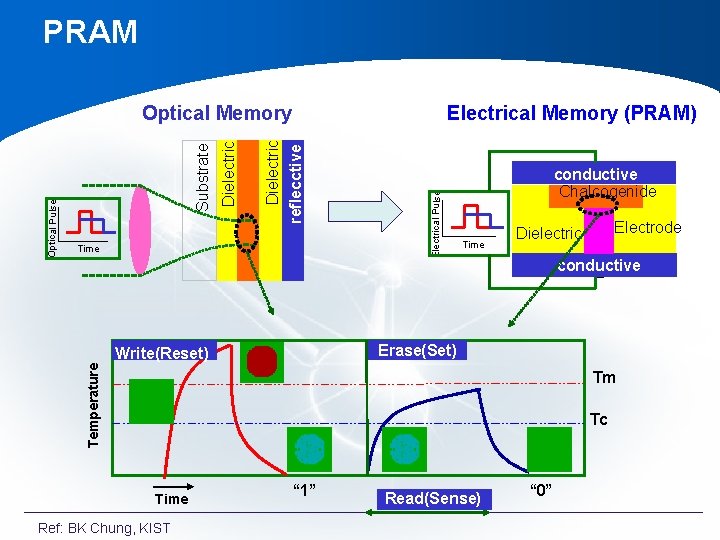
PRAM Time Electrical Memory (PRAM) Electrical Pulse Dielectric reflecctive Dielectric Substrate Optical Pulse Optical Memory conductive Chalcogenide Time Electrode Dielectric conductive 2 Erase(Set) Temperature Write(Reset) Tm Tc Time Ref: BK Chung, KIST “ 1” Read(Sense) “ 0”
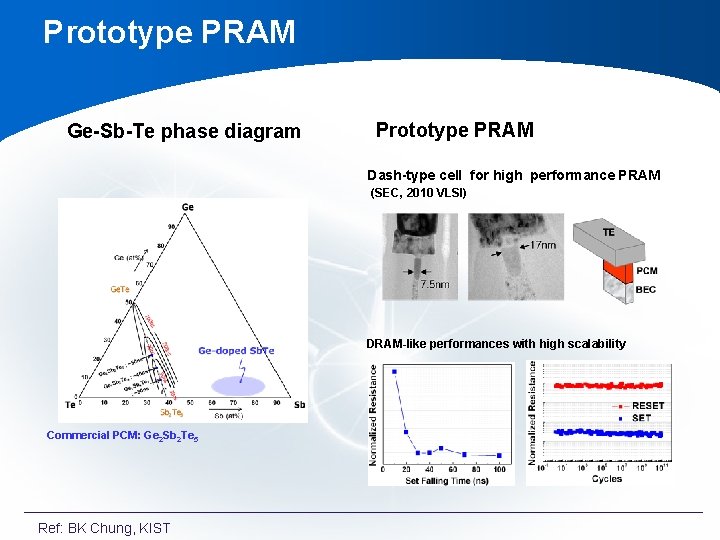
Prototype PRAM Ge-Sb-Te phase diagram Prototype PRAM Dash-type cell for high performance PRAM (SEC, 2010 VLSI) DRAM-like performances with high scalability Commercial PCM: Ge 2 Sb 2 Te 5 Ref: BK Chung, KIST
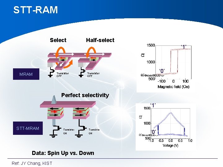
STT-RAM Select Half-select ‘ 1’ MRAM Transistor OFF ‘ 0’ Transistor OFF Perfect selectivity ‘ 1’ STT-MRAM Transistor ON ON Data: Spin Up vs. Down Ref: JY Chang, KIST ‘ 0’
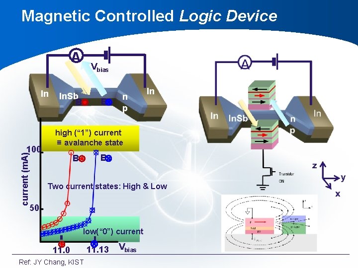
Magnetic Controlled Logic Device A In current (m. A) 100 Vbias In. Sb B B R 1 n p In high (“ 1”) current ≡ avalanche state B B Two current states: High & Low 50 low(“ 0”) current 11. 0 Ref: JY Chang, KIST 11. 13 Vbias R 2
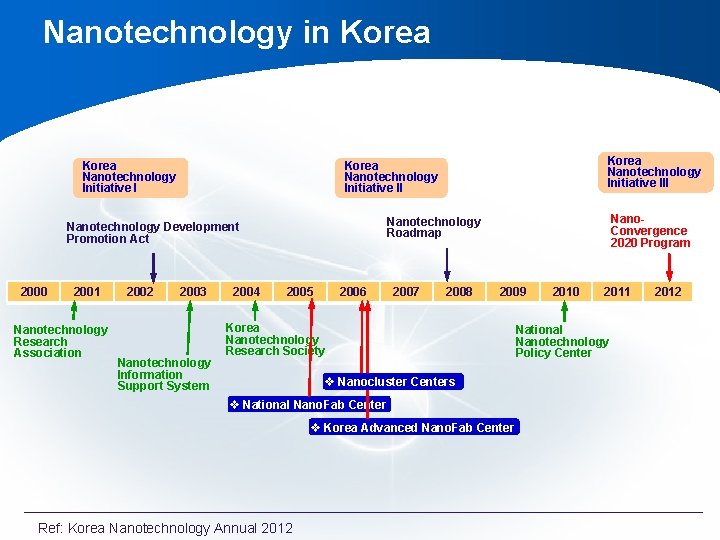
Nanotechnology in Korea Nanotechnology Initiative I 2001 Nanotechnology Research Association 2002 2003 Nanotechnology Information Support System 2004 Nano. Convergence 2020 Program Nanotechnology Roadmap Nanotechnology Development Promotion Act 2000 Korea Nanotechnology Initiative III Korea Nanotechnology Initiative II 2005 2006 2007 2008 Korea Nanotechnology Research Society 2009 2011 National Nanotechnology Policy Center v Nanocluster Centers v National Nano. Fab Center v Korea Advanced Nano. Fab Center Ref: Korea Nanotechnology Annual 2012 2010 2012
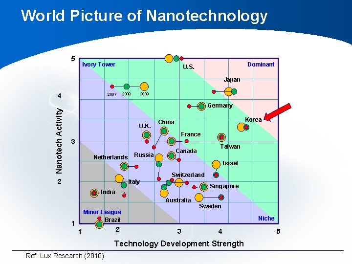
World Picture of Nanotechnology 5 Ivory Tower Dominant U. S. Japan Nanotech Activity 4 2007 2008 2009 Germany U. K. Korea China France 3 Netherlands Russia Taiwan Canada Israel Switzerland 2 Italy Singapore India Australia Minor League Brazil 1 1 2 Sweden Niche 3 4 Technology Development Strength Ref: Lux Research (2010) 5
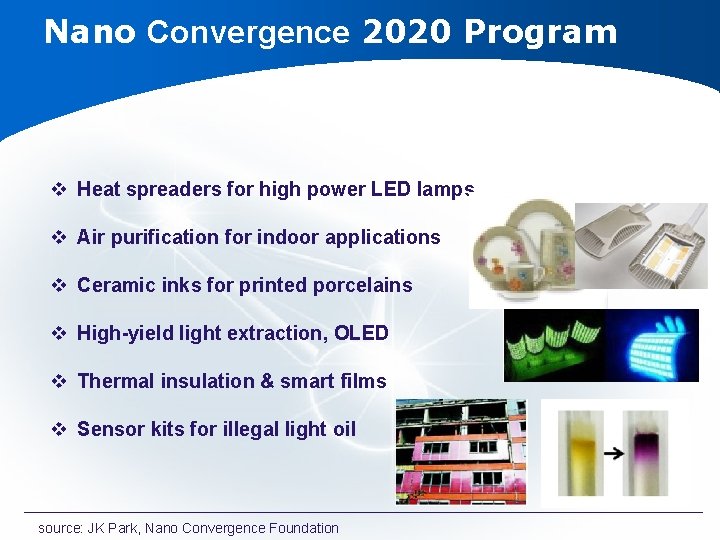
Nano Convergence 2020 Program v Heat spreaders for high power LED lamps v Air purification for indoor applications v Ceramic inks for printed porcelains v High-yield light extraction, OLED v Thermal insulation & smart films v Sensor kits for illegal light oil source: JK Park, Nano Convergence Foundation
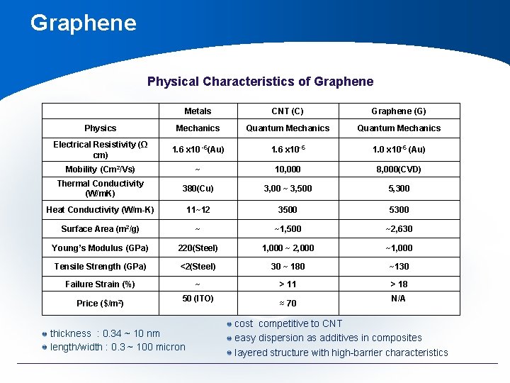
Graphene Physical Characteristics of Graphene Metals CNT (C) Graphene (G) Physics Mechanics Quantum Mechanics Electrical Resistivity (Ω cm) 1. 6 x 10 -6(Au) 1. 6 x 10 -6 1. 0 x 10 -6 (Au) Mobility (Cm 2/Vs) ~ 10, 000 8, 000(CVD) Thermal Conductivity (W/m. K) 380(Cu) 3, 00 ~ 3, 500 5, 300 Heat Conductivity (W/m-K) 11~12 3500 5300 Surface Area (m 2/g) ~ ~1, 500 ~2, 630 Young’s Modulus (GPa) 220(Steel) 1, 000 ~ 2, 000 ~1, 000 Tensile Strength (GPa) <2(Steel) 30 ~ 180 ~130 Failure Strain (%) ~ > 11 > 18 Price ($/m 2) 50 (ITO) thickness : 0. 34 ~ 10 nm length/width : 0. 3 ~ 100 micron ≈ 70 N/A cost competitive to CNT easy dispersion as additives in composites layered structure with high-barrier characteristics
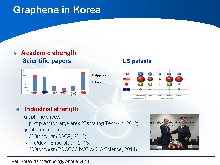
Graphene in Korea Academic strength Scientific papers US patents l Application l Basic Industrial strength graphene sheets : - pilot plant for large area (Samsung Techwin, 2012) graphene nanoplatelets : - 300 ton/year (SSCP, 2013) - 1 kg/day (Enbarotech, 2013) - 200 ton/year (POSCO/HWC w/ XG Science, 2014) Ref: Korea Nanotechnology Annual 2011
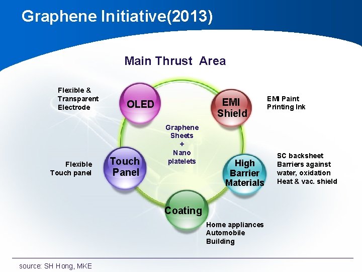
Graphene Initiative(2013) Main Thrust Area Flexible & Transparent Electrode Flexible Touch panel EMI Shield OLED Touch Panel Graphene Sheets + Nano platelets High Barrier Materials Coating Home appliances Automobile Building source: SH Hong, MKE EMI Paint Printing Ink SC backsheet Barriers against water, oxidation Heat & vac. shield
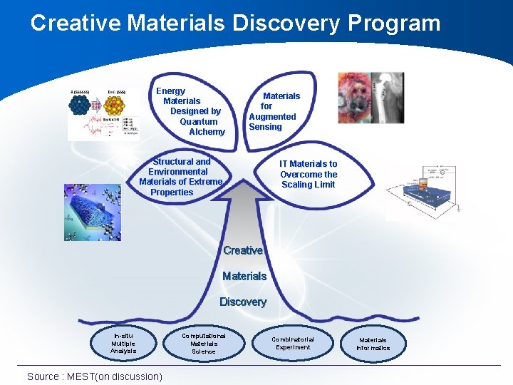
Creative Materials Discovery Program Energy Materials Designed by Quantum Alchemy Materials for Augmented Sensing Structural and Environmental Materials of Extreme Properties IT Materials to Overcome the Scaling Limit Creative Materials Discovery In-situ Multiple Analysis Source : MEST(on discussion) Computational Materials Science Combinatorial Experiment Materials Informatics
Summary & Conclusion u Materials technology has made remarkable progress through continuous evolution in Korea. u Innovation in materials and processing technology makes the bread-earning industries competitive. u Translational R/D to bridge the valley of death is strongly emphasized. u Group efforts covering all value chains is strongly asked in Government R/D of key materials and components. u Coordination of inter- & multi-disciplinary corperation becomes more important in newly converging fields (IT+NT+BT).
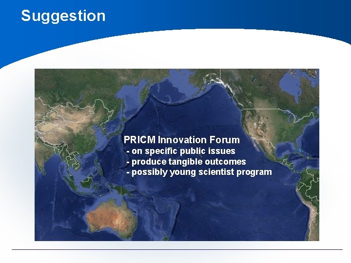
Suggestion PRICM Innovation Forum - on specific public issues - produce tangible outcomes - possibly young scientist program