
New 500 MSas 12 bit FADC in VME

New 500 MSa/s 12 bit FADC in VME Sangyeol Kim Notice Co. , Ltd.
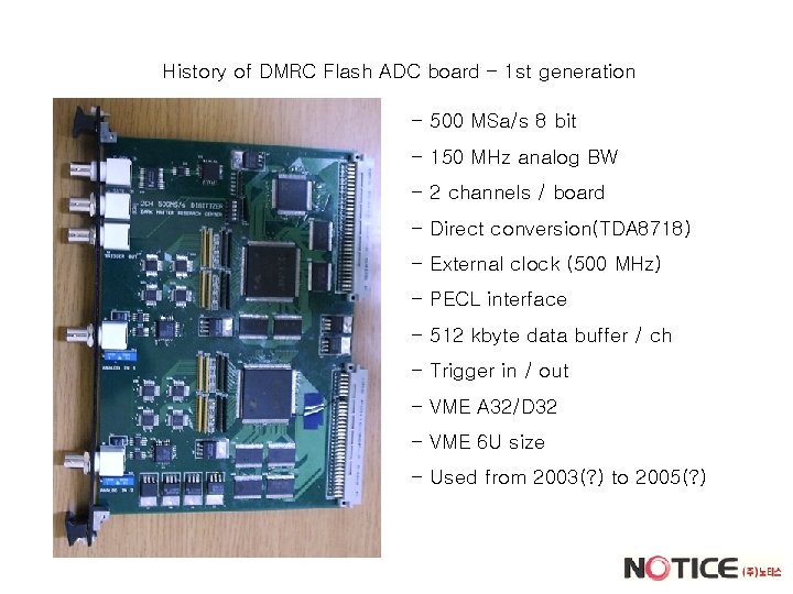
History of DMRC Flash ADC board – 1 st generation - 500 MSa/s 8 bit - 150 MHz analog BW - 2 channels / board - Direct conversion(TDA 8718) - External clock (500 MHz) - PECL interface - 512 kbyte data buffer / ch - Trigger in / out - VME A 32/D 32 - VME 6 U size - Used from 2003(? ) to 2005(? )
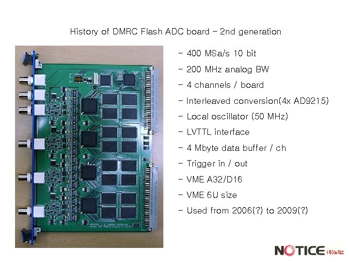
History of DMRC Flash ADC board – 2 nd generation - 400 MSa/s 10 bit - 200 MHz analog BW - 4 channels / board - Interleaved conversion(4 x AD 9215) - Local oscillator (50 MHz) - LVTTL interface - 4 Mbyte data buffer / ch - Trigger in / out - VME A 32/D 16 - VME 6 U size - Used from 2006(? ) to 2009(? )
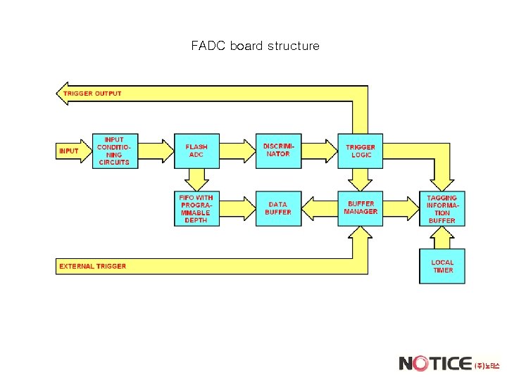
FADC board structure
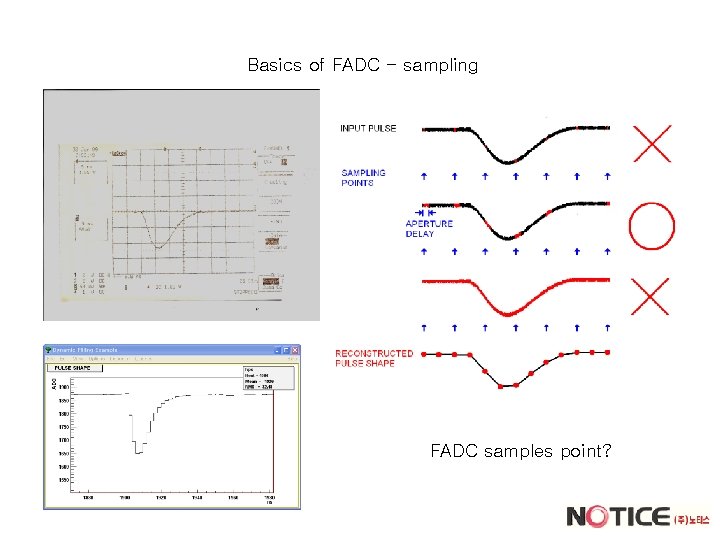
Basics of FADC - sampling FADC samples point?

Basics of FADC Bits, sampling rate & BW
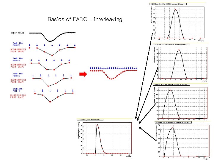
Basics of FADC - interleaving
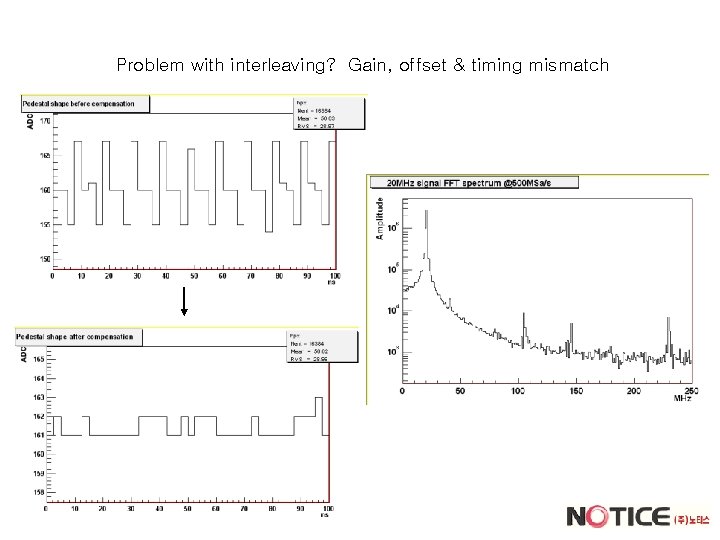
Problem with interleaving? Gain, offset & timing mismatch
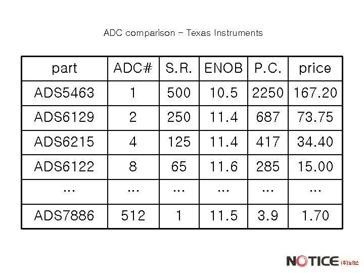
ADC comparison – Texas Instruments part ADC# S. R. ENOB P. C. price ADS 5463 1 500 10. 5 2250 167. 20 ADS 6129 2 250 11. 4 687 73. 75 ADS 6215 4 125 11. 4 417 34. 40 ADS 6122 8 65 11. 6 285 15. 00 … … … 512 1 11. 5 3. 9 1. 70 … ADS 7886
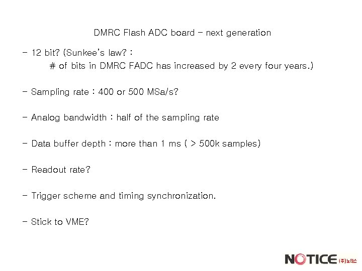
DMRC Flash ADC board – next generation - 12 bit? (Sunkee’s law? : # of bits in DMRC FADC has increased by 2 every four years. ) - Sampling rate : 400 or 500 MSa/s? - Analog bandwidth : half of the sampling rate - Data buffer depth : more than 1 ms ( > 500 k samples) - Readout rate? - Trigger scheme and timing synchronization. - Stick to VME?
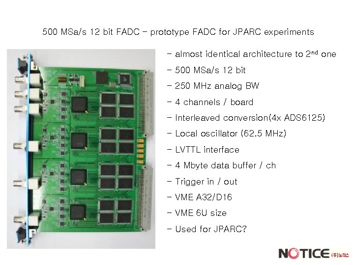
500 MSa/s 12 bit FADC – prototype FADC for JPARC experiments - almost identical architecture to 2 nd one - 500 MSa/s 12 bit - 250 MHz analog BW - 4 channels / board - Interleaved conversion(4 x ADS 6125) - Local oscillator (62. 5 MHz) - LVTTL interface - 4 Mbyte data buffer / ch - Trigger in / out - VME A 32/D 16 - VME 6 U size - Used for JPARC?
- Slides: 11