Network for Computational Nanotechnology NCN Berkeley Univ of
Network for Computational Nanotechnology (NCN) Berkeley, Univ. of Illinois, Norfolk State, Northwestern, Purdue, UTEP OMEN: a Quantum Transport Modeling Tool for Nanoelectronic Devices Mathieu Luisier and Gerhard Klimeck
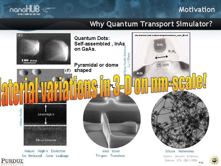
Motivation Why Quantum Transport Simulator? Pyramidal or dome shaped 45 nm Node R. Leon et al, JPL (1998) 65 nm Node Devices LG=35 nm Quantum Dots: Self-assembled , In. As on Ga. As. http: //download. intel. com/technology/silicon_paper_06. pdf
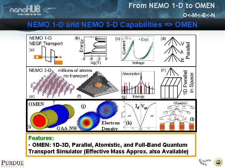
From NEMO 1 -D to OMEN O<-M<-E<-N NEMO 1 -D and NEMO 3 -D Capabilities => OMEN (i) (j) GAA NW Id-Vgs Electron Density (k) Features: • OMEN: 1 D-3 D, Parallel, Atomistic, and Full-Band Quantum Transport Simulator (Effective Mass Approx. also Available) (l)
Overview • Introduction and Motivation Why Quantum Transport? What is OMEN? • Application to Devices NW FETs MIT In. As HEMTs Graphene Nanoribbon TFET • Summary and Outlook
Overview • Introduction and Motivation Why Quantum Transport? What is OMEN? • Application to Devices NW FETs MIT In. As HEMTs Graphene Nanoribbon TFETs • Outlook
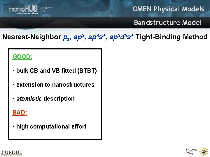
OMEN Physical Models Bandstructure Model Nearest-Neighbor pz, sp 3 s*, sp 3 d 5 s* Tight-Binding Method GOOD: • bulk CB and VB fitted (BTBT) • extension to nanostructures • atomistic description BAD: • high computational effort
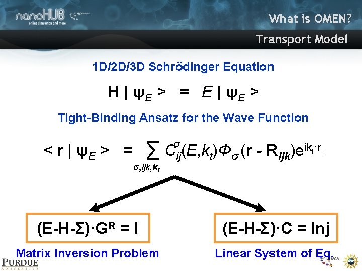
What is OMEN? Transport Model 1 D/2 D/3 D Schrödinger Equation H | ψE > = E | ψE > Tight-Binding Ansatz for the Wave Function ∑ Cij(E, kt)Φσ (r - Rijk)eik ·r σ < r | ψE > = t t σ, ijk, kt (E-H-Σ)·GR = I (E-H-Σ)·C = Inj Matrix Inversion Problem Linear System of Eq.
Overview • Introduction and Motivation Why Quantum Transport? What is OMEN? • Application to Devices NW FETs MIT In. As HEMTs Graphene Nanoribbon TFETs • Outlook
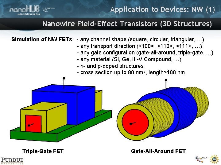
Application to Devices: NW (1) Nanowire Field-Effect Transistors (3 D Structures) Simulation of NW FETs: - any channel shape (square, circular, triangular, …) - any transport direction (<100>, <111>, …) - any gate configuration (gate-all-around, triple-gate, …) - any material (Si, Ge, III-V Compound, …) - n- and p-doped structures - cross section up to 80 nm 2, length>100 nm Triple-Gate FET Gate-All-Around FET
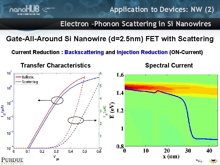
Application to Devices: NW (2) Electron –Phonon Scattering in Si Nanowires Gate-All-Around Si Nanowire (d=2. 5 nm) FET with Scattering Current Reduction : Backscattering and Injection Reduction (ON-Current) Transfer Characteristics Spectral Current
Overview • Introduction and Motivation Why Quantum Transport? What is OMEN? • Application to Devices NW FETs MIT In. As HEMTs Graphene Nanoribbon TFETs • Outlook
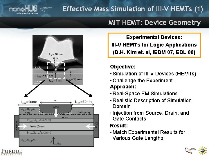
Effective Mass Simulation of III-V HEMTs (1) MIT HEMT: Device Geometry Experimental Devices: III-V HEMTs for Logic Applications (D. H. Kim et. al, IEDM 07, EDL 08) Objective: • Simulation of III-V Devices (HEMTs) • Challenge the Experiment Approach: • Real-Space EM Simulations • Realistic Description of Simulation Domain • Injection from Source, Drain, and Gate Contacts Result: • Match Experimental Results for Various Gate Lengths
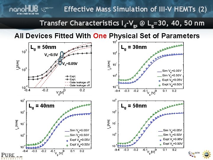
Effective Mass Simulation of III-V HEMTs (2) Transfer Characteristics Id-Vgs @ Lg=30, 40, 50 nm All Devices Fitted With One Physical Set of Parameters Lg = 50 nm Lg = 30 nm Vd=0. 5 V Vd=0. 05 V Lg = 40 nm Lg = 50 nm
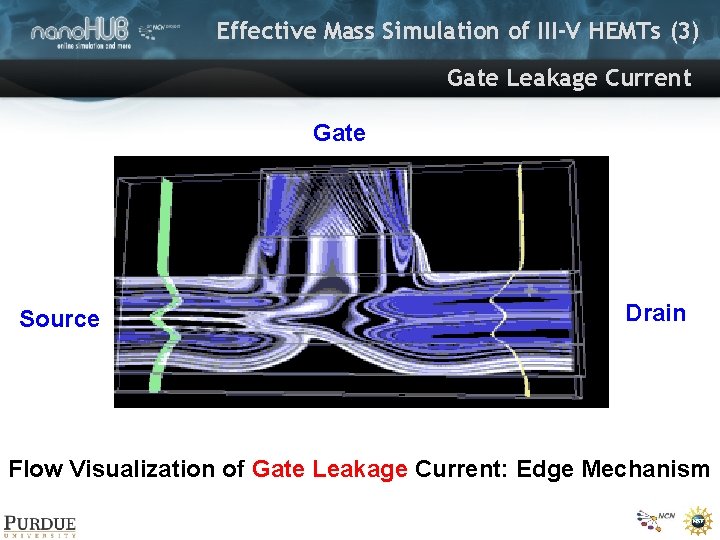
Effective Mass Simulation of III-V HEMTs (3) Gate Leakage Current Gate Source Drain Flow Visualization of Gate Leakage Current: Edge Mechanism
Overview • Introduction and Motivation Why Quantum Transport? What is OMEN? • Application to Devices NW FETs MIT In. As HEMTs Graphene Nanoribbon TFETs • Outlook
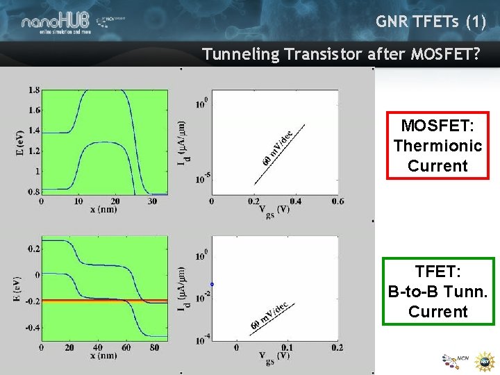
GNR TFETs (1) Tunneling Transistor after MOSFET? MOSFET: Thermionic Current TFET: B-to-B Tunn. Current
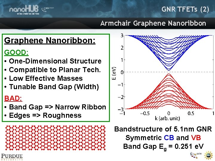
GNR TFETs (2) Armchair Graphene Nanoribbon: GOOD: • One-Dimensional Structure • Compatible to Planar Tech. • Low Effective Masses • Tunable Band Gap (Width) BAD: • Band Gap => Narrow Ribbon • Edges => Roughness Bandstructure of 5. 1 nm GNR Symmetric CB and VB Band Gap Eg = 0. 251 e. V
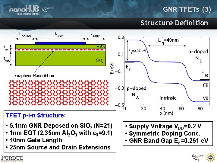
GNR TFETs (3) Structure Definition TFET p-i-n Structure: • 5. 1 nm GNR Deposed on Si. O 2 (N=21) • 1 nm EOT (2. 35 nm Al 2 O 3 with εR=9. 1) • 40 nm Gate Length • 25 nm Source and Drain Extensions • Supply Voltage VDD=0. 2 V • Symmetric Doping Conc. • GNR Band Gap Eg=0. 251 e. V
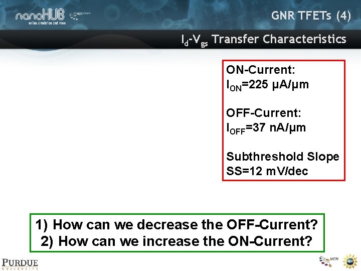
GNR TFETs (4) Id-Vgs Transfer Characteristics ON-Current: ION=225 μA/μm OFF-Current: IOFF=37 n. A/μm Subthreshold Slope SS=12 m. V/dec 1) How can we decrease the OFF-Current? 2) How can we increase the ON-Current?
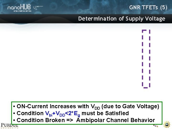
GNR TFETs (5) Determination of Supply Voltage • ON-Current Increases with VDD (due to Gate Voltage) • Condition Vbi+VDD<2*Eg must be Satisfied • Condition Broken => Ambipolar Channel Behavior
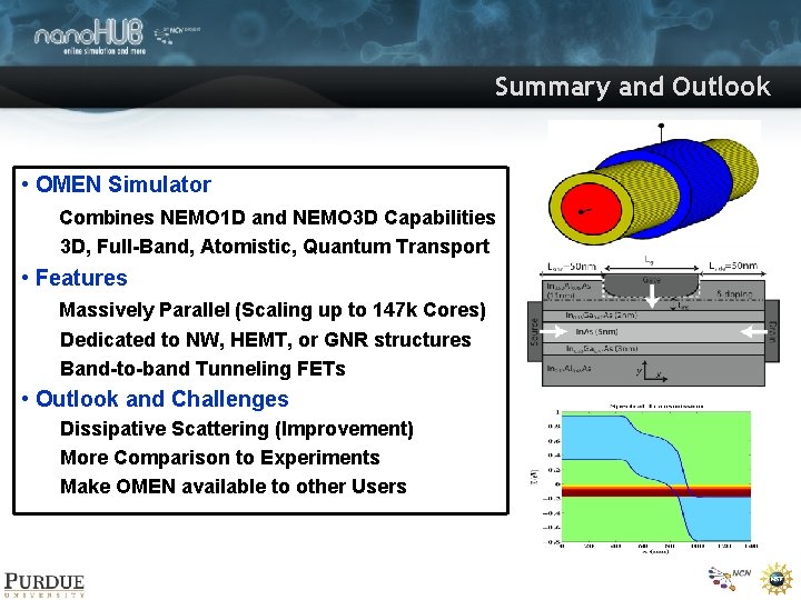
Summary and Outlook • OMEN Simulator Combines NEMO 1 D and NEMO 3 D Capabilities 3 D, Full-Band, Atomistic, Quantum Transport • Features Massively Parallel (Scaling up to 147 k Cores) Dedicated to NW, HEMT, or GNR structures Band-to-band Tunneling FETs • Outlook and Challenges Dissipative Scattering (Improvement) More Comparison to Experiments Make OMEN available to other Users
- Slides: 21