Negative Bias Temperature Instability NBTI in p MOSFETs
Negative Bias Temperature Instability (NBTI) in p. MOSFETs: Characterization, Material/Process Dependence and Predictive Modeling (Part 1 of 3) Souvik Mahapatra Department of Electrical Engineering Indian Institute of Technology Bombay, Mumbai, India Email: souvik@ee. iitb. ac. in; mahapatra. souvik@gmail. com Co-contributors: M. A. Alam & A. E. Islam (Purdue), E. N. Kumar, V. D. Maheta, S. Deora, G. Kapila, D. Varghese, K. Joshi & N. Goel (IIT Bombay) Acknowledgement: C. Olsen and K. Ahmed (Applied Materials), H. Aono, E. Murakami (Renesas), G. Bersuker (SEMATECH), CEN IIT Bombay, NCN Purdue, Applied Materials, Renesas Electronics, SEMATECH, SRC / GRC 1
Outline Introduction, Basic NBTI signatures Fast / Ultra-fast drain current degradation measurement Part-I Estimation of pre-existing and generated defects Transistor process / material dependence Part-II Role of Nitrogen – Study by Ultrafast measurement Predictive modeling Part-III Conclusions / outlook 2
Outline Introduction, Basic NBTI signatures Fast / Ultra-fast drain current degradation measurement Estimation of pre-existing and generated defects Transistor process / material dependence Role of Nitrogen – Study by Ultrafast measurement Predictive modeling Conclusions / outlook 3
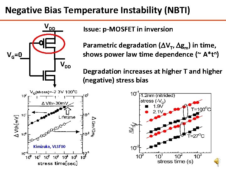
Negative Bias Temperature Instability (NBTI) VDD VG=0 Issue: p-MOSFET in inversion Parametric degradation (DVT, Dgm) in time, shows power law time dependence (~ A*tn) VDD Degradation increases at higher T and higher (negative) stress bias Kimizuka, VLSI’ 00 4
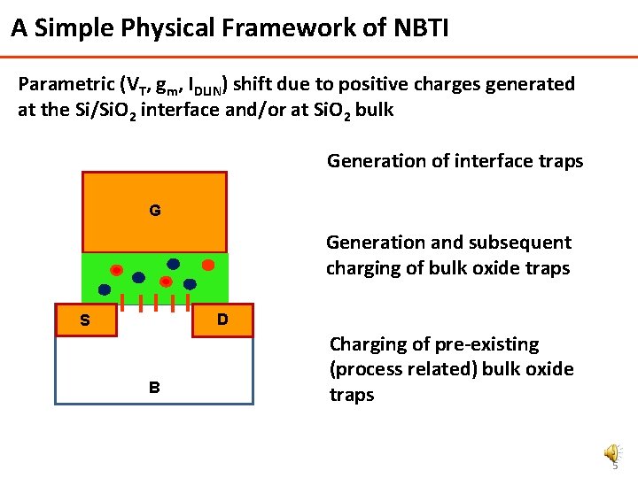
A Simple Physical Framework of NBTI Parametric (VT, gm, IDLIN) shift due to positive charges generated at the Si/Si. O 2 interface and/or at Si. O 2 bulk Generation of interface traps G Generation and subsequent charging of bulk oxide traps D S B Charging of pre-existing (process related) bulk oxide traps 5
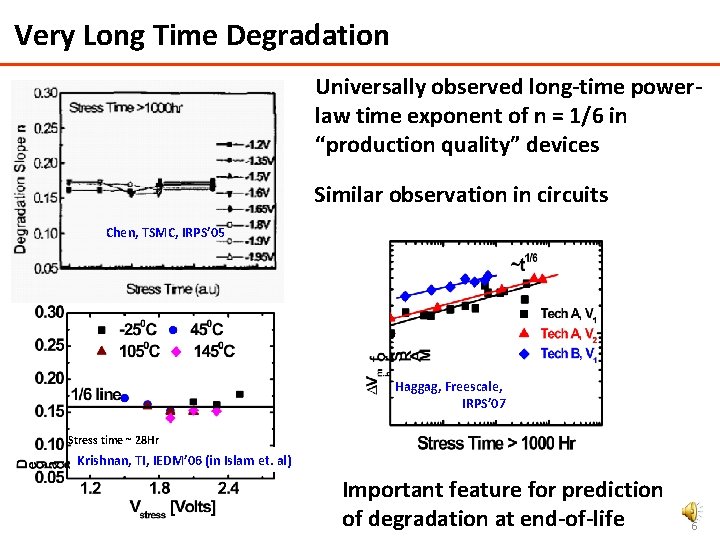
Very Long Time Degradation Universally observed long-time powerlaw time exponent of n = 1/6 in “production quality” devices Similar observation in circuits Chen, TSMC, IRPS’ 05 Haggag, Freescale, IRPS’ 07 Stress time ~ 28 Hr Krishnan, TI, IEDM’ 06 (in Islam et. al) Important feature for prediction of degradation at end-of-life 6
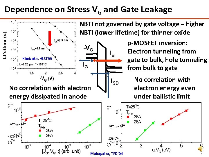
Dependence on Stress VG and Gate Leakage NBTI not governed by gate voltage – higher NBTI (lower lifetime) for thinner oxide -VG Kimizuka, VLSI’ 99 IB IG No correlation with electron energy dissipated in anode ISD Mahapatra, TED’ 04 p-MOSFET inversion: Electron tunneling from gate to bulk, hole tunneling from bulk to gate No correlation with electron energy even under ballistic limit 7
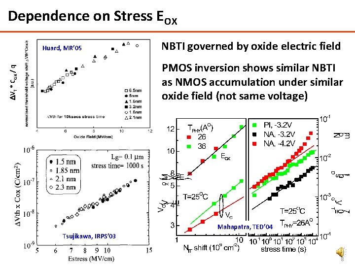
Dependence on Stress EOX Huard, MR’ 05 NBTI governed by oxide electric field DVT * COX / q PMOS inversion shows similar NBTI as NMOS accumulation under similar oxide field (not same voltage) Mahapatra, TED’ 04 Tsujikawa, IRPS’ 03 8
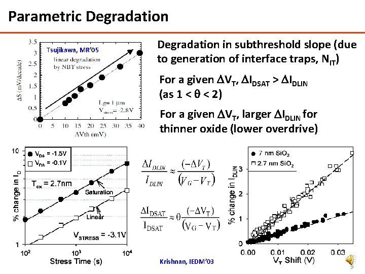
Parametric Degradation Tsujikawa, MR’ 05 Degradation in subthreshold slope (due to generation of interface traps, NIT) For a given DVT, DIDSAT > DIDLIN (as 1 < < 2) For a given DVT, larger DIDLIN for thinner oxide (lower overdrive) Krishnan, IEDM’ 03 9
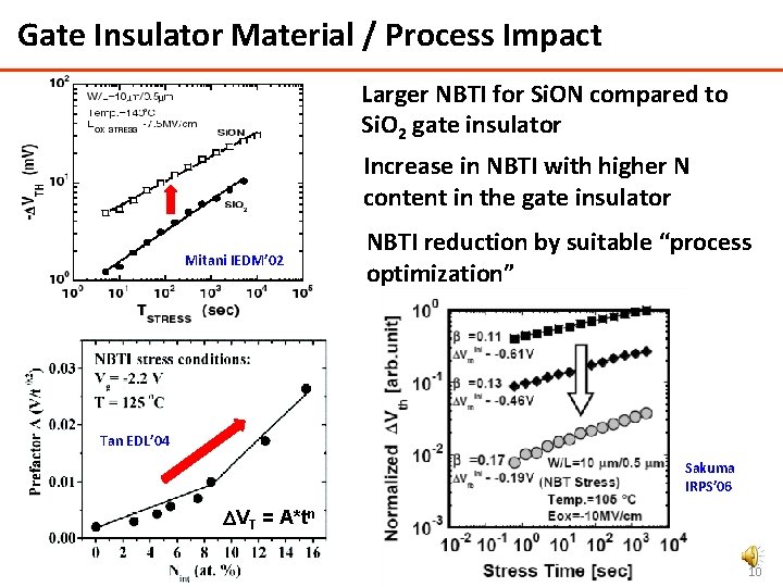
Gate Insulator Material / Process Impact Larger NBTI for Si. ON compared to Si. O 2 gate insulator Increase in NBTI with higher N content in the gate insulator Mitani IEDM’ 02 NBTI reduction by suitable “process optimization” Tan EDL’ 04 Sakuma IRPS’ 06 DVT = A*tn 10
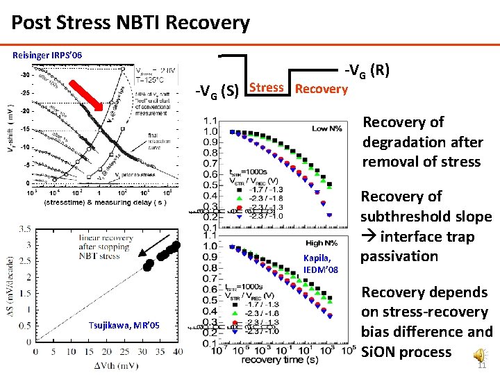
Post Stress NBTI Recovery Reisinger IRPS’ 06 -VG (R) -VG (S) Stress Recovery of degradation after removal of stress Kapila, IEDM’ 08 Tsujikawa, MR’ 05 Recovery of subthreshold slope interface trap passivation Recovery depends on stress-recovery bias difference and Si. ON process 11
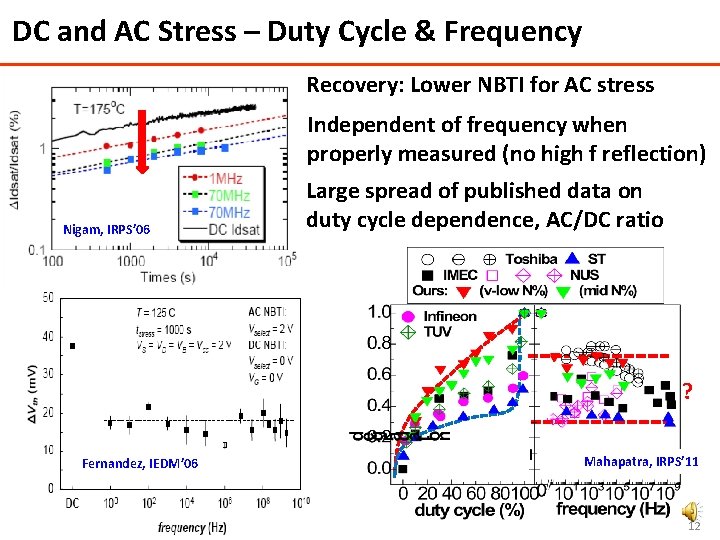
DC and AC Stress – Duty Cycle & Frequency Recovery: Lower NBTI for AC stress Independent of frequency when properly measured (no high f reflection) Nigam, IRPS’ 06 Large spread of published data on duty cycle dependence, AC/DC ratio ? Fernandez, IEDM’ 06 Mahapatra, IRPS’ 11 12
Motivation Explanation of the following features: Strong gate insulator process dependence Time evolution of degradation, prediction at long time Temperature and oxide field dependence of degradation Recovery of degradation after DC stress Duty cycle and frequency dependence under AC stress Understanding and estimation of defects responsible for degradation under accelerated stress condition Predictive modeling for lifetime projection – extrapolation of shorttime accelerated stress data to end-of-life under use condition 13
Outline Introduction, Basic NBTI signatures Fast / Ultra-fast drain current degradation measurement Estimation of pre-existing and generated defects Transistor process / material dependence Role of Nitrogen – Study by Ultrafast measurement Predictive modeling Conclusions / outlook 14

Issues with Measure-Stress-Measure Approach Unintentional recovery during measurement delay Lower magnitude & higher slope (n) Measurement -VG (M) due to recovery during measure delay Stress Increase in slope (n) with higher T and -VG (S) higher measure delay – artifact M-time Need “delay-free” measurement Varghese, IEDM’ 05 15
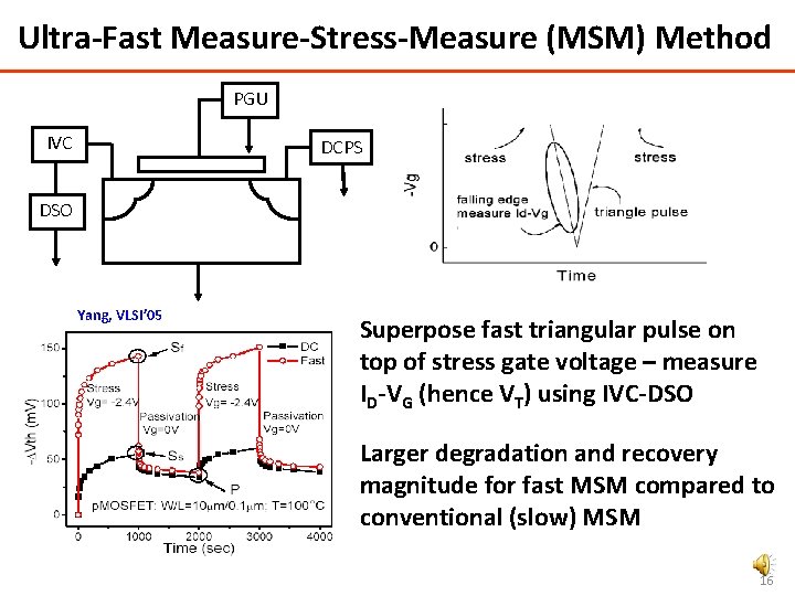
Ultra-Fast Measure-Stress-Measure (MSM) Method PGU IVC DCPS DSO Yang, VLSI’ 05 Superpose fast triangular pulse on top of stress gate voltage – measure ID-VG (hence VT) using IVC-DSO Larger degradation and recovery magnitude for fast MSM compared to conventional (slow) MSM 16
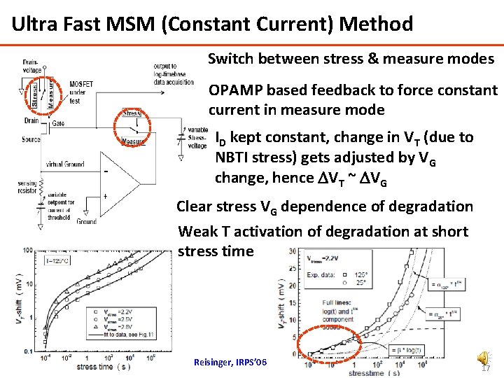
Ultra Fast MSM (Constant Current) Method Switch between stress & measure modes OPAMP based feedback to force constant current in measure mode ID kept constant, change in VT (due to NBTI stress) gets adjusted by VG change, hence DVT ~ DVG Clear stress VG dependence of degradation Weak T activation of degradation at short stress time Reisinger, IRPS’ 06 17
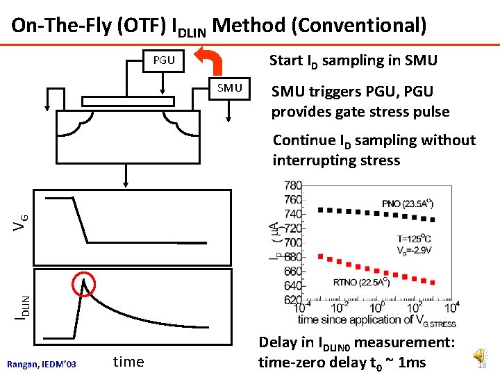
On-The-Fly (OTF) IDLIN Method (Conventional) Start ID sampling in SMU PGU SMU triggers PGU, PGU provides gate stress pulse IDLIN VG Continue ID sampling without interrupting stress Rangan, IEDM’ 03 time Delay in IDLIN 0 measurement: time-zero delay t 0 ~ 1 ms 18
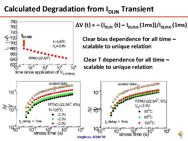
Calculated Degradation from IDLIN Transient DV (t) = – (IDLIN (t) – IDLIN 0 (1 ms))/IDLIN 0 (1 ms) IDLIN 0 Clear bias dependence for all time – scalable to unique relation Clear T dependence for all time – scalable to unique relation Varghese, IEDM’ 05 19
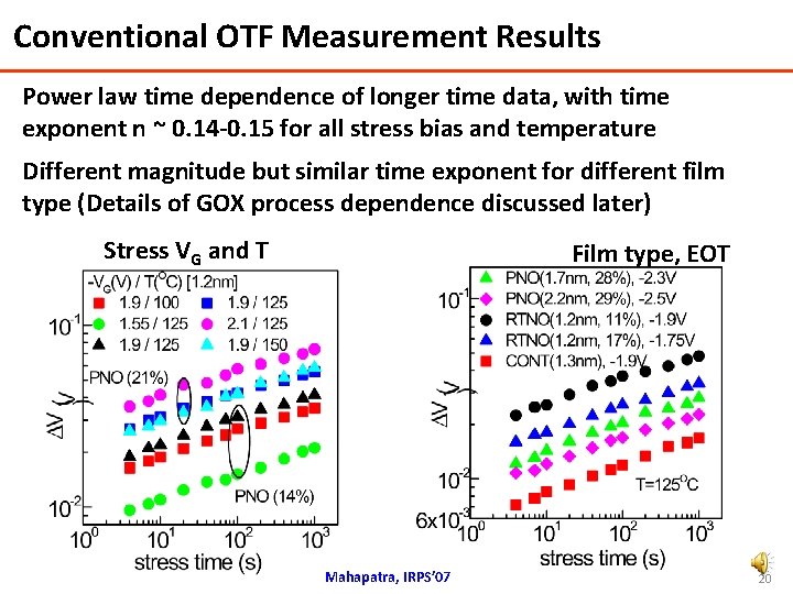
Conventional OTF Measurement Results Power law time dependence of longer time data, with time exponent n ~ 0. 14 -0. 15 for all stress bias and temperature Different magnitude but similar time exponent for different film type (Details of GOX process dependence discussed later) Stress VG and T Film type, EOT Mahapatra, IRPS’ 07 20
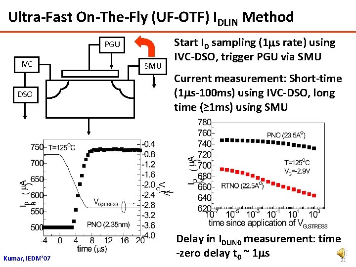
Ultra-Fast On-The-Fly (UF-OTF) IDLIN Method PGU IVC DSO Kumar, IEDM’ 07 SMU Start ID sampling (1 ms rate) using IVC-DSO, trigger PGU via SMU Current measurement: Short-time (1 ms-100 ms) using IVC-DSO, long time (≥ 1 ms) using SMU Delay in IDLIN 0 measurement: time -zero delay t 0 ~ 1 ms 21
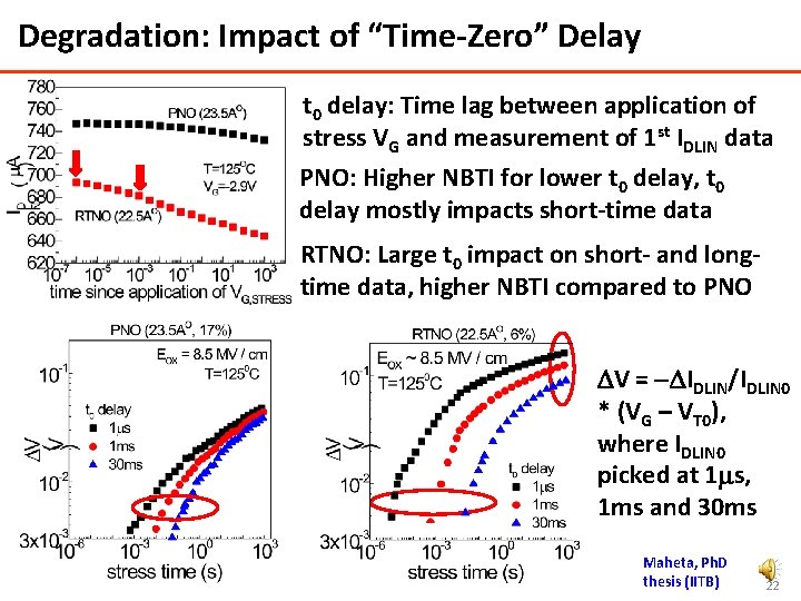
Degradation: Impact of “Time-Zero” Delay t 0 delay: Time lag between application of stress VG and measurement of 1 st IDLIN data PNO: Higher NBTI for lower t 0 delay, t 0 delay mostly impacts short-time data RTNO: Large t 0 impact on short- and longtime data, higher NBTI compared to PNO DV = -DIDLIN/IDLIN 0 * (VG – VT 0), where IDLIN 0 picked at 1 ms, 1 ms and 30 ms Maheta, Ph. D thesis (IITB) 22
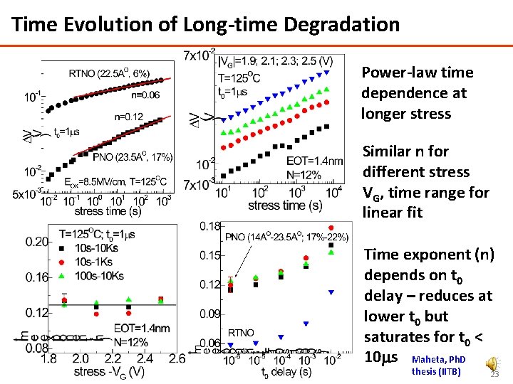
Time Evolution of Long-time Degradation Power-law time dependence at longer stress Similar n for different stress VG, time range for linear fit Time exponent (n) depends on t 0 delay – reduces at lower t 0 but saturates for t 0 < 10 ms Maheta, Ph. D thesis (IITB) 23
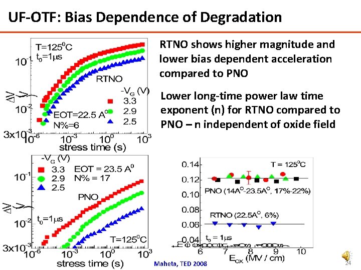
UF-OTF: Bias Dependence of Degradation RTNO shows higher magnitude and lower bias dependent acceleration compared to PNO Lower long-time power law time exponent (n) for RTNO compared to PNO – n independent of oxide field Maheta, TED 2008 24
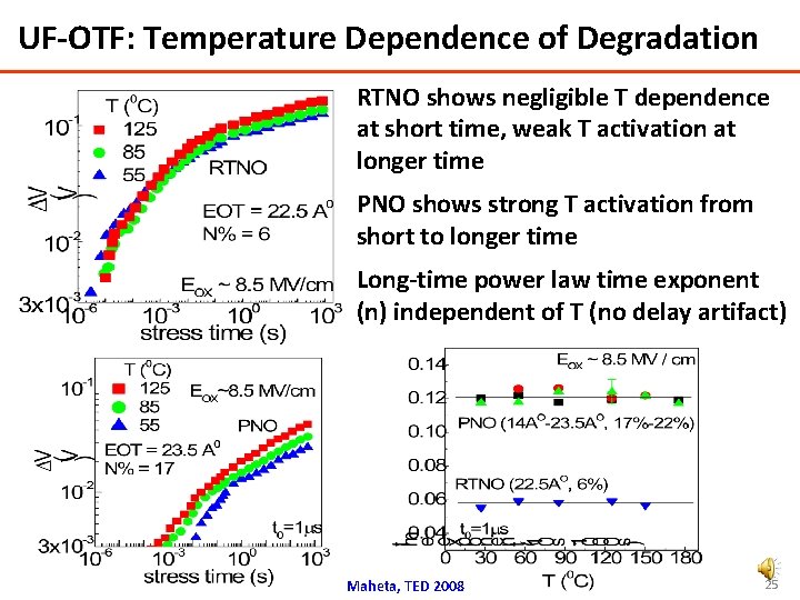
UF-OTF: Temperature Dependence of Degradation RTNO shows negligible T dependence at short time, weak T activation at longer time PNO shows strong T activation from short to longer time Long-time power law time exponent (n) independent of T (no delay artifact) Maheta, TED 2008 25
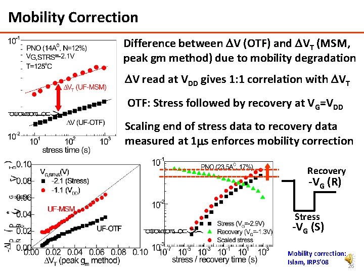
Mobility Correction Difference between DV (OTF) and DVT (MSM, peak gm method) due to mobility degradation DV read at VDD gives 1: 1 correlation with DVT OTF: Stress followed by recovery at VG=VDD Scaling end of stress data to recovery data measured at 1 ms enforces mobility correction Recovery -VG (R) Stress -VG (S) Mobility correction: Islam, IRPS’ 08 26
Summary Recovery of NBTI degradation after removal of stress – issues with conventional “slow” MSM methods Ultrafast MSM can provide VT shift with negligible artifacts, is useful for capturing long time degradation for lifetime determination, early part (t<1 s) degradation cannot be studied Constant current ultrafast MSM method is an alternative, but needs subthreshold slope correction to determine proper VT shift On-the-fly (OTF) IDLIN methods can be used to study degradation from 1 ms (fast version) and 1 ms (ultra-fast version) time scale Important process dependent signatures observed in sub ms time scale by UF-OTF method (discussed in detail later) OTF IDLIN needs mobility correction to obtain VT shift 27
Outline Introduction, Basic NBTI signatures Fast / Ultra-fast drain current degradation measurement Estimation of pre-existing and generated defects Transistor process / material dependence Role of Nitrogen – Study by Ultrafast measurement Predictive modeling Conclusions / outlook 28
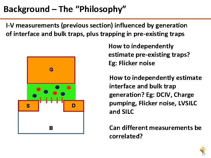
Background – The “Philosophy” I-V measurements (previous section) influenced by generation of interface and bulk traps, plus trapping in pre-existing traps How to independently estimate pre-existing traps? Eg: Flicker noise G D S B How to independently estimate interface and bulk trap generation? Eg: DCIV, Charge pumping, Flicker noise, LVSILC and SILC Can different measurements be correlated? 29
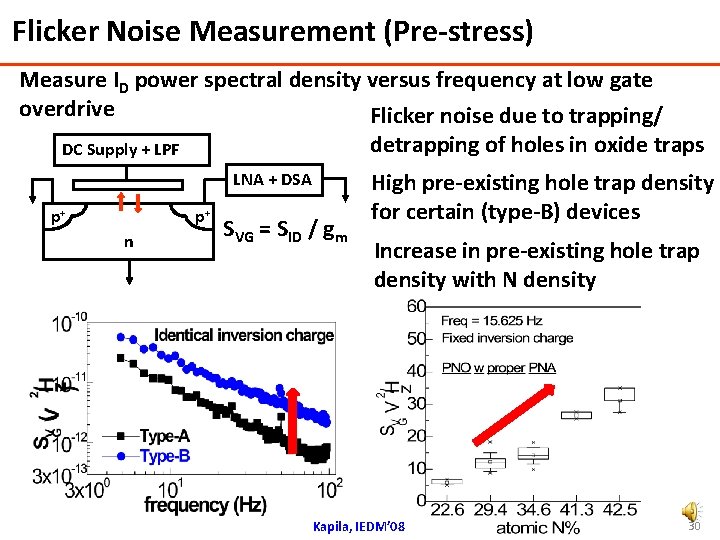
Flicker Noise Measurement (Pre-stress) Measure ID power spectral density versus frequency at low gate overdrive Flicker noise due to trapping/ detrapping of holes in oxide traps DC Supply + LPF LNA + DSA p+ p+ n SVG = SID / gm High pre-existing hole trap density for certain (type-B) devices Increase in pre-existing hole trap density with N density Kapila, IEDM’ 08 30

DCIV Measurements Sweep VG with S/D in F. B, measure ISUB due to electron-hole recombination in traps at or near Si/Si. O 2 interface VF p+ p+ n ISUB Increase in ISUB due to stress seen in both Si. O 2 and Si. ON: Indicates trap generation at or near Si/Si. O 2 interface Neugroschel, MR’ 07 Stathis IRPS’ 04 Stress time 31
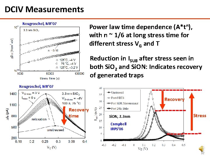
DCIV Measurements Neugroschel, MR’ 07 Power law time dependence (A*tn), with n ~ 1/6 at long stress time for different stress VG and T Reduction in ISUB after stress seen in both Si. O 2 and Si. ON: Indicates recovery of generated traps Neugroschel, MR’ 07 Recovery time Si. ON, 2. 3 nm Stress Campbell IRPS’ 06 32
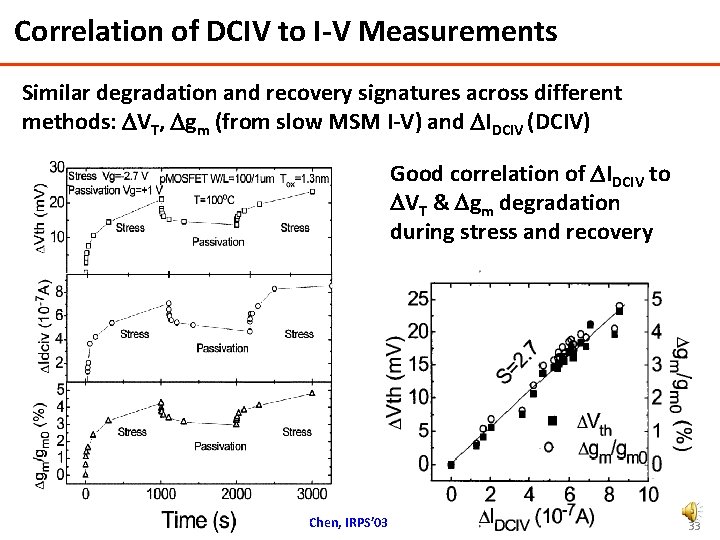
Correlation of DCIV to I-V Measurements Similar degradation and recovery signatures across different methods: DVT, Dgm (from slow MSM I-V) and DIDCIV (DCIV) Good correlation of DIDCIV to DVT & Dgm degradation during stress and recovery Chen, IRPS’ 03 33
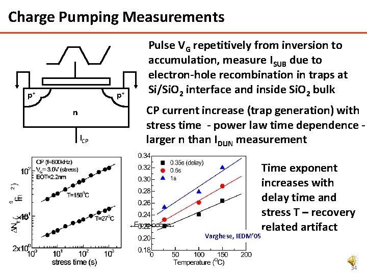
Charge Pumping Measurements p+ p+ n ICP Pulse VG repetitively from inversion to accumulation, measure ISUB due to electron-hole recombination in traps at Si/Si. O 2 interface and inside Si. O 2 bulk CP current increase (trap generation) with stress time - power law time dependence larger n than IDLIN measurement Varghese, IEDM’ 05 Time exponent increases with delay time and stress T – recovery related artifact 34
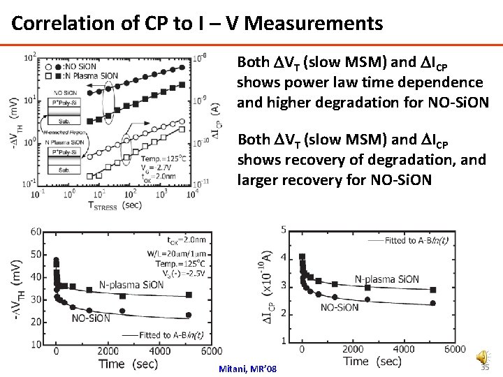
Correlation of CP to I – V Measurements Both DVT (slow MSM) and DICP shows power law time dependence and higher degradation for NO-Si. ON Both DVT (slow MSM) and DICP shows recovery of degradation, and larger recovery for NO-Si. ON Mitani, MR’ 08 35
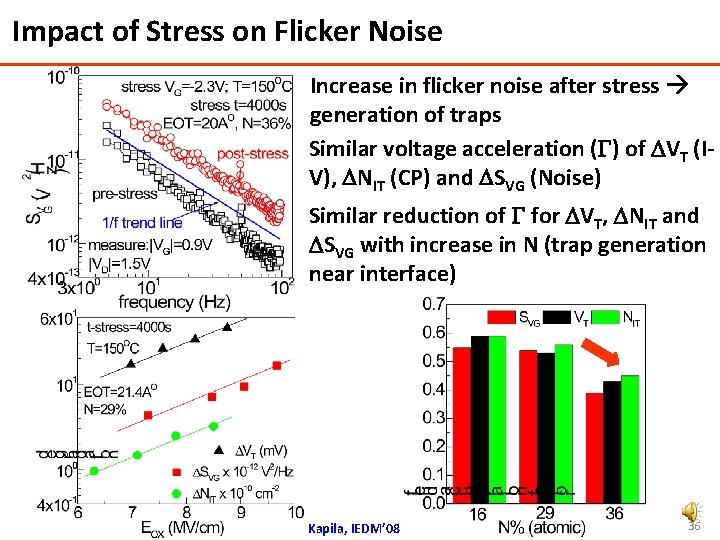
Impact of Stress on Flicker Noise Increase in flicker noise after stress generation of traps Similar voltage acceleration (G) of DVT (IV), DNIT (CP) and DSVG (Noise) Similar reduction of G for DVT, DNIT and DSVG with increase in N (trap generation near interface) Kapila, IEDM’ 08 36
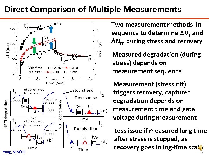
Direct Comparison of Multiple Measurements Two measurement methods in sequence to determine DVT and DNIT during stress and recovery Measured degradation (during stress) depends on measurement sequence Measurement (stress off) triggers recovery, captured degradation depends on measurement time and gate voltage during measurement Yang, VLSI’ 05 Less issue if measured long time after stress is stopped, as recovery goes in log-time scale 37
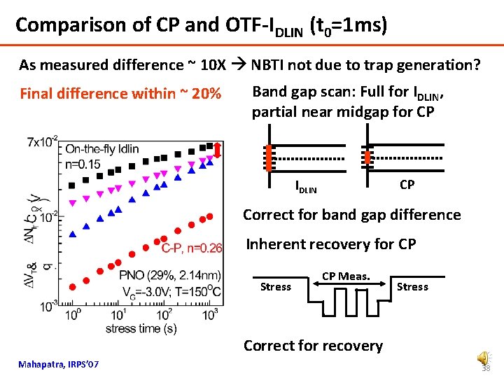
Comparison of CP and OTF-IDLIN (t 0=1 ms) As measured difference ~ 10 X NBTI not due to trap generation? Final difference within ~ 20% Band gap scan: Full for IDLIN, partial near midgap for CP CP IDLIN Correct for band gap difference Inherent recovery for CP Stress CP Meas. Stress Correct for recovery Mahapatra, IRPS’ 07 38
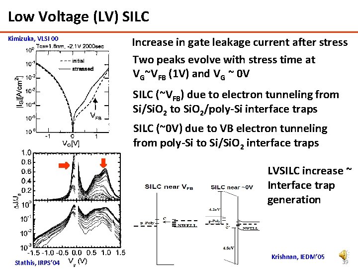
Low Voltage (LV) SILC Kimizuka, VLSI 00 Increase in gate leakage current after stress Two peaks evolve with stress time at VG~VFB (1 V) and VG ~ 0 V SILC (~VFB) due to electron tunneling from Si/Si. O 2 to Si. O 2/poly-Si interface traps SILC (~0 V) due to VB electron tunneling from poly-Si to Si/Si. O 2 interface traps LVSILC increase ~ Interface trap generation Stathis, IRPS’ 04 Krishnan, IEDM’ 05 39
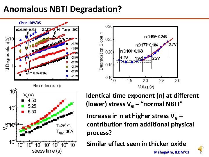
Anomalous NBTI Degradation? Chen IRPS’ 05 Identical time exponent (n) at different (lower) stress VG – “normal NBTI” Increase in n at higher stress VG – contribution from additional physical process? Similar effect seen in thicker oxide Mahapatra, IEDM’ 02 40
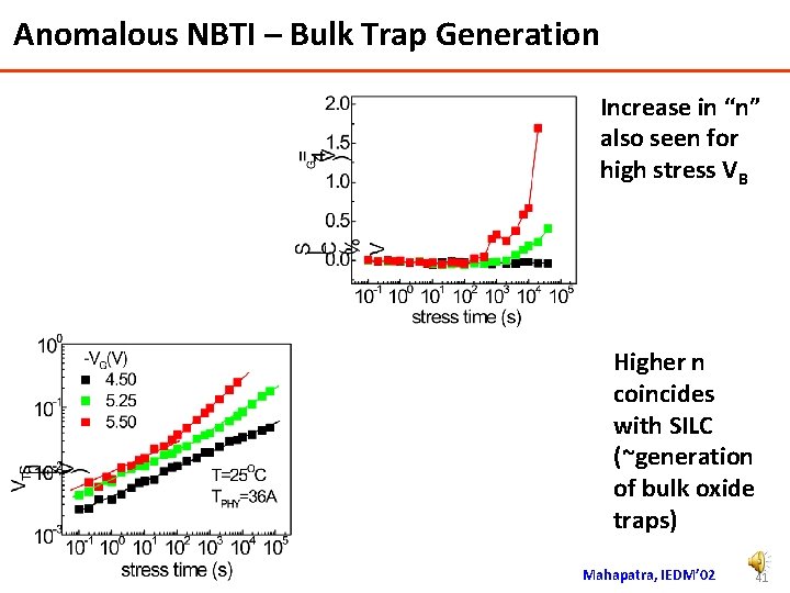
Anomalous NBTI – Bulk Trap Generation Increase in “n” also seen for high stress VB Higher n coincides with SILC (~generation of bulk oxide traps) Mahapatra, IEDM’ 02 41
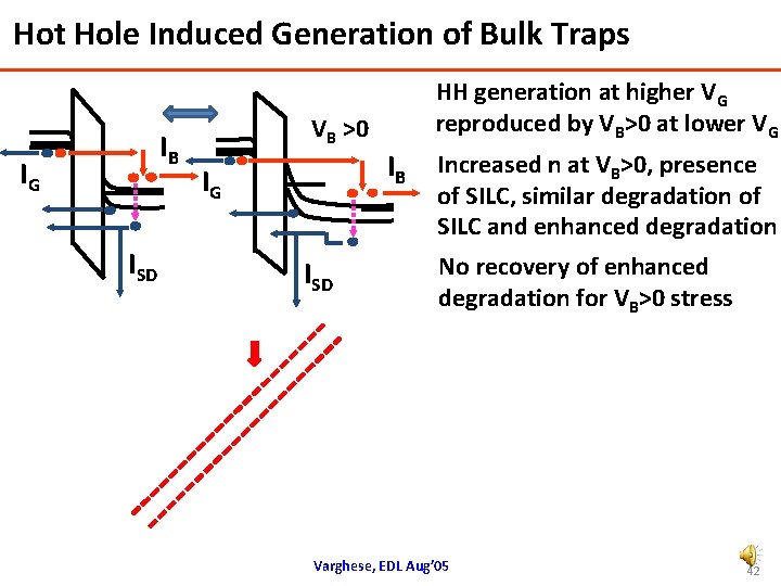
Hot Hole Induced Generation of Bulk Traps IB IG ISD VB >0 IG ISD HH generation at higher VG reproduced by VB>0 at lower VG IB Increased n at VB>0, presence of SILC, similar degradation of SILC and enhanced degradation No recovery of enhanced degradation for VB>0 stress Varghese, EDL Aug’ 05 42
Summary NBTI: Generation of interface traps, charging of pre-existing and generated bulk traps Differently processed devices show difference in pre-existing bulk traps (Flicker noise on pre-stressed devices) Interface / near interface and bulk trap generation signatures shown by multiple measurements Evidence of interface / near interface trap generation from DCIV, high frequency charge pumping, LVSILC Evidence of bulk trap generation from HVSILC Several important factors need to be carefully considered if attempts are made to compare multiple measurements 43
Outline Introduction, Basic NBTI signatures Fast / Ultra-fast drain current degradation measurement Estimation of pre-existing and generated defects Transistor process / material dependence Go to Part – II Role of Nitrogen – Study by Ultrafast measurement Predictive modeling Conclusions / outlook 44
- Slides: 44