NEEP 541 Ionization in Semiconductors II Fall 2002
- Slides: 10

NEEP 541 Ionization in Semiconductors - II Fall 2002 Jake Blanchard

Outline n Radiation effects in Semiconductors n n n Ionization Recombination Trapping Junctions Example

Ionization Due to Radiation n n n When semiconductor is subjected to ionizing radiation (photons or charged particles) with energy greater than the bandgap, electrons are excited from the valence band to the conduction band This creates an electron hole pair This increases electrons in conduction band (excess carriers) If transferred energy exceeds the bandgap, the excess goes to heating 3. 7 e. V needed to create electron hole pair in Si (bandgap is about 1. 1 e. V) This is not sensitive to temperature

Ionization effects (continued) n n One effect of the excess carriers is an increase in the electrical conductivity There does not seem to be any difference between electrons and holes produced by ionizing radiation and those which are naturally present in the semiconductor

Recombination n n When the radiation stops, the electrons and holes will begin to recombine and revert to their equilibrium densities Recombination mechanisms n n Direct reaction between electron and hole (this is how LEDs emit light) – not important in Si and Ge, but important in Ga. As In Si and Ge, an intermediate (defect) energy level captures either a hole or an electron, then captures the opposite type of carrier

Trapping n n When defect densities are large and one carrier type is more easily captured than the other, then the excess densities are no longer equal. This is called minority carrier trapping This leads to very long-lived excess electrical conductivity For example, if holes are captured, then the excess electrons remain in conduction band for a long time

P-N junctions n n Ionizing radiation creates a current in a PN junction (“primary photocurrent”) There is a prompt current that is coincident with the radiation and a delayed current that occurs after the radiation stops The prompt current is from electron hole pairs created in the depleted region of the junction The delayed current is from the minority carriers produced in the bulk diffusing to the junction

Solar Cells n n A solar cell is a PN junction designed for optimum collection of sunlight Typically 0. 5 microns of n-type on 250 microns p-type

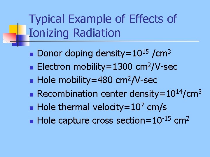
Typical Example of Effects of Ionizing Radiation n n n Donor doping density=1015 /cm 3 Electron mobility=1300 cm 2/V-sec Hole mobility=480 cm 2/V-sec Recombination center density=1014/cm 3 Hole thermal velocity=107 cm/s Hole capture cross section=10 -15 cm 2

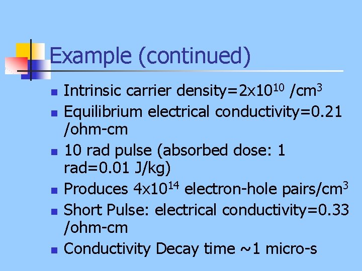
Example (continued) n n n Intrinsic carrier density=2 x 10¹⁰ /cm 3 Equilibrium electrical conductivity=0. 21 /ohm-cm 10 rad pulse (absorbed dose: 1 rad=0. 01 J/kg) Produces 4 x 10¹⁴ electron-hole pairs/cm 3 Short Pulse: electrical conductivity=0. 33 /ohm-cm Conductivity Decay time ~1 micro-s