
NC STATE UNIVERSITY Free PDK 15 An OpenSource
- Slides: 17
NC STATE UNIVERSITY Free. PDK 15 An Open-Source Predictive Process Design Kit for 15 nm Fin. FET Technology Kirti Bhanushali, W. Rhett Davis (NCSU) International Symposium on Physical Design April 1, 2015 Slide 1 © 2015 Bhanushali & Davis
Motivation l Problem » Restrictions on PDKs prevent sharing of design data, impede research & teaching l Solution » Free Predictive PDK, establishes a baseline for research & teaching in design, architecture, manufacturing, and automation l Free. PDK 45 accomplished this for 45 nm, Free. PDK 15 seeks to do the same for 15 nm Slide 2 © 2015 Bhanushali & Davis
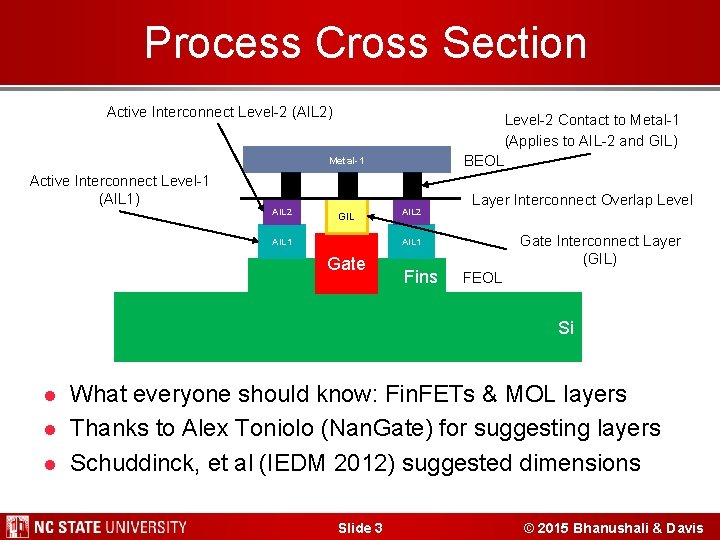
Process Cross Section • Active Interconnect Level-2 (AIL 2) • Level-2 Contact to Metal-1 • (Applies to AIL-2 and GIL) • BEOL Metal-1 • Active Interconnect Level-1 (AIL 1) AIL 2 GIL AIL 1 AIL 2 • Layer Interconnect Overlap Level • Gate Interconnect Layer (GIL) AIL 1 Gate Fins • FEOL Si l l l What everyone should know: Fin. FETs & MOL layers Thanks to Alex Toniolo (Nan. Gate) for suggesting layers Schuddinck, et al (IEDM 2012) suggested dimensions Slide 3 © 2015 Bhanushali & Davis
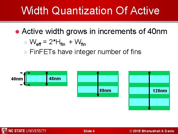
Width Quantization Of Active l Active width grows in increments of 40 nm » Weff = 2*Hfin + Wfin » Fin. FETs have integer number of fins 40 nm • 48 nm 88 nm Slide 4 128 nm © 2015 Bhanushali & Davis
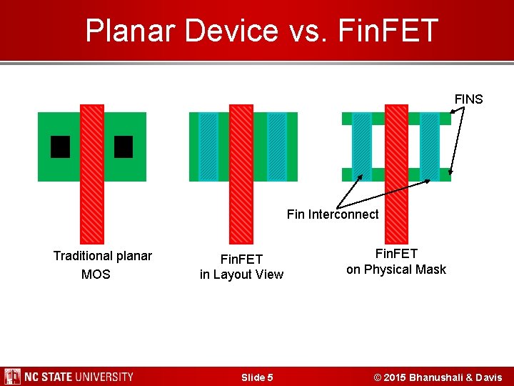
Planar Device vs. Fin. FET • FINS • Fin Interconnect • Traditional planar • MOS Fin. FET in Layout View Slide 5 Fin. FET on Physical Mask © 2015 Bhanushali & Davis
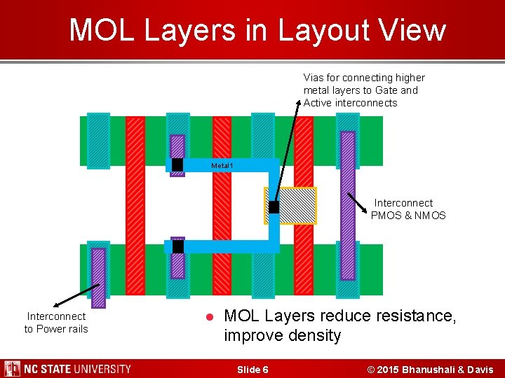
MOL Layers in Layout View Vias for connecting higher metal layers to Gate and Active interconnects Metal 1 • Interconnect PMOS & NMOS Interconnect to Power rails l MOL Layers reduce resistance, improve density Slide 6 © 2015 Bhanushali & Davis
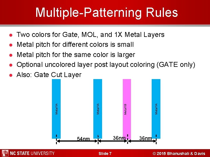
Multiple-Patterning Rules l • 54 nm Metal 1 A l Metal 1 B l Metal 1 A l Two colors for Gate, MOL, and 1 X Metal Layers Metal pitch for different colors is small Metal pitch for the same color is larger Optional uncolored layer post layout coloring (GATE only) Also: Gate Cut Layer Metal 1 A l • 36 nm Slide 7 • 36 nm © 2015 Bhanushali & Davis
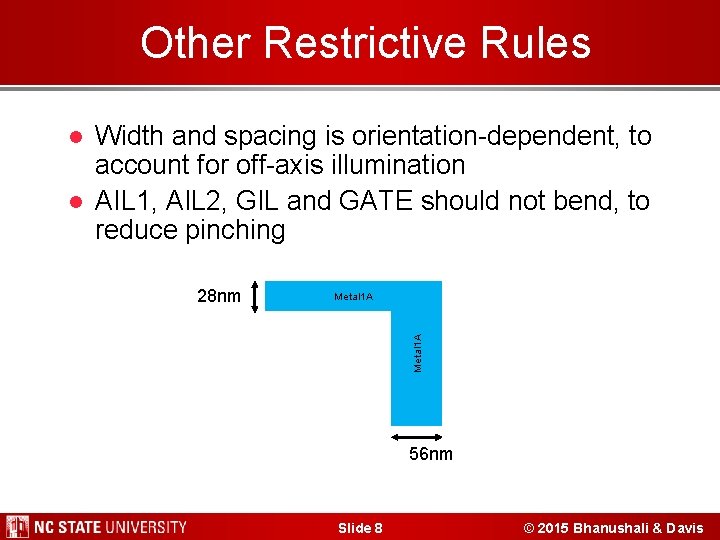
Other Restrictive Rules l Width and spacing is orientation-dependent, to account for off-axis illumination AIL 1, AIL 2, GIL and GATE should not bend, to reduce pinching • 28 nm Metal 1 A l • 56 nm Slide 8 © 2015 Bhanushali & Davis
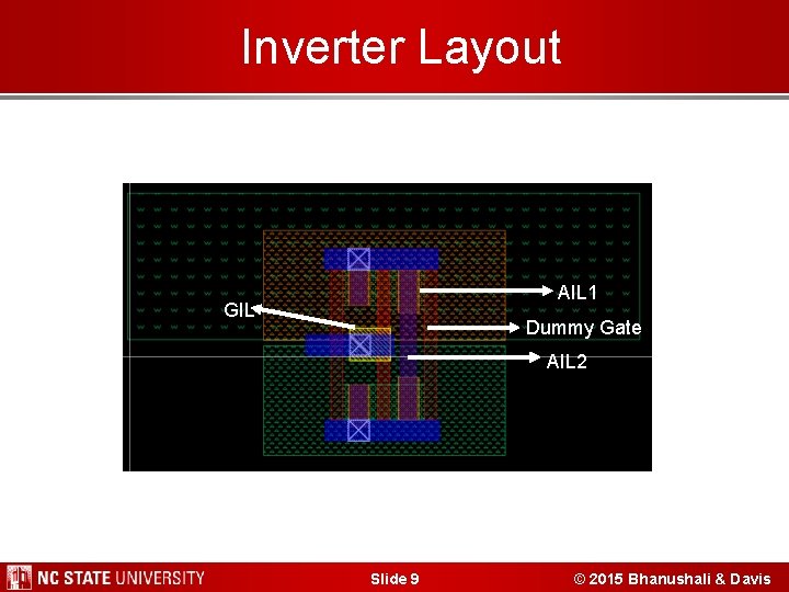
Inverter Layout – Inverter AIL 1 GIL Dummy Gate AIL 2 Slide 9 © 2015 Bhanushali & Davis
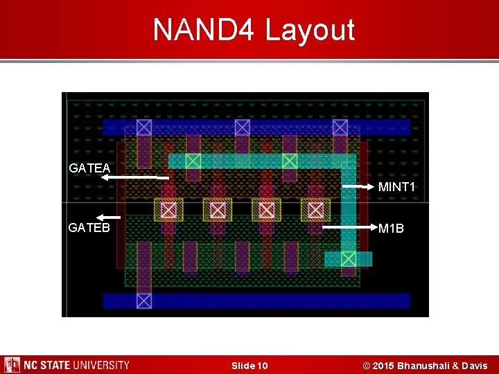
NAND 4 Layout NAND 4 GATEA MINT 1 GATEB M 1 B Slide 10 © 2015 Bhanushali & Davis
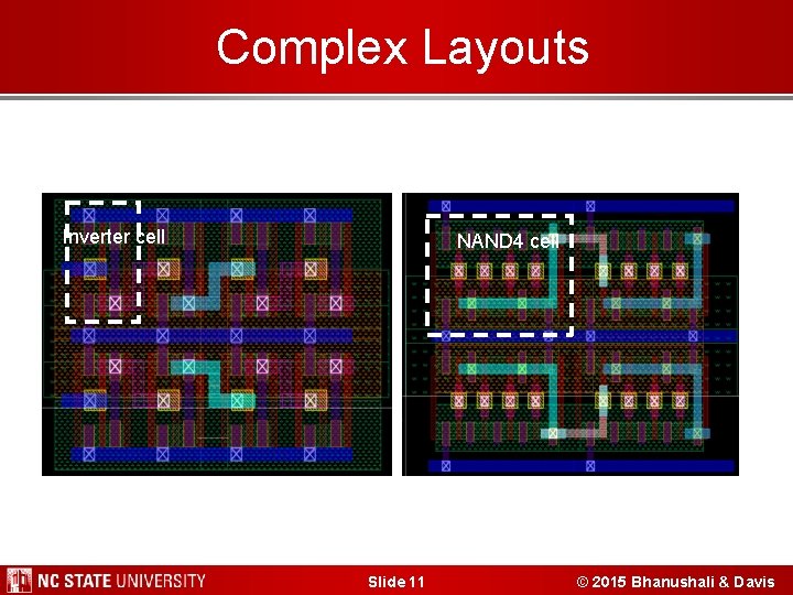
Complex Layouts Inverter cell NAND 4 cell Slide 11 © 2015 Bhanushali & Davis
Density Evaluation l Fin. FET inverter @14 nm : MOS Inverter @45 nm Layout Density Comparison » Ideal shrink factor- 1: 9 » Achieved shrink factor- 1: 6 l l Fin. FET layout density is 1. 3 x MOSFET (Alioto, ICM 2009) Cause » Width Quantization » Higher Hfin for same Weff Slide 12 © 2015 Bhanushali & Davis
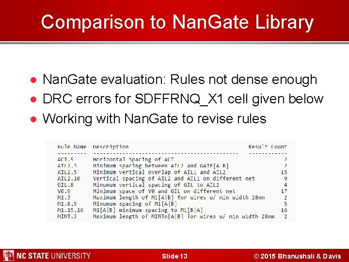
Comparison to Nan. Gate Library l l l Nan. Gate evaluation: Rules not dense enough DRC errors for SDFFRNQ_X 1 cell given below Working with Nan. Gate to revise rules Slide 13 © 2015 Bhanushali & Davis
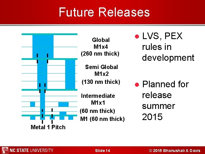
Future Releases Global M 1 x 4 (260 nm thick) Semi Global M 1 x 2 (130 nm thick) Intermediate M 1 x 1 (60 nm thick) M 1 (60 nm thick) l LVS, PEX rules in development l Planned for release summer 2015 Metal 1 Pitch Slide 14 © 2015 Bhanushali & Davis
Licensing l Licensed for Academic Use under 3 -clause BSD License » Caveat: Cannot distribute a Cell Library until Summer 2016 l Please contact us for commercial license » Click through license may be possible with your help Slide 15 © 2015 Bhanushali & Davis
Conclusion l First-pass Free. PDK 15 with DRC is now available, including new 15 nm features » Fin. FETs » MOL Layers » Multiple Patterning l l LVS & PEX rules available in summer How you can help » Feedback on design rules » Request a commercial use license Slide 16 © 2015 Bhanushali & Davis
Acknowledgements Acknowledgement Alex Toniolo l Joseph Davis, Tarek Ramadan, Ahmed Hammed Fathy, Omar El-Sewefy , Ahmed El-Kordy, Hend Wagieh (Mentor Graphics) l Slide 17 © 2015 Bhanushali & Davis