NANOTECHNOLOGY Part 3 Optics Microoptics NearField Optics Scanning

- Slides: 23

NANOTECHNOLOGY Part 3. Optics • • Micro-optics Near-Field Optics Scanning Near-Field Optical Microscopy Surface Plasmons J. R. Krenn – Nanotechnology – CERN 2003 – Part 3 page 1

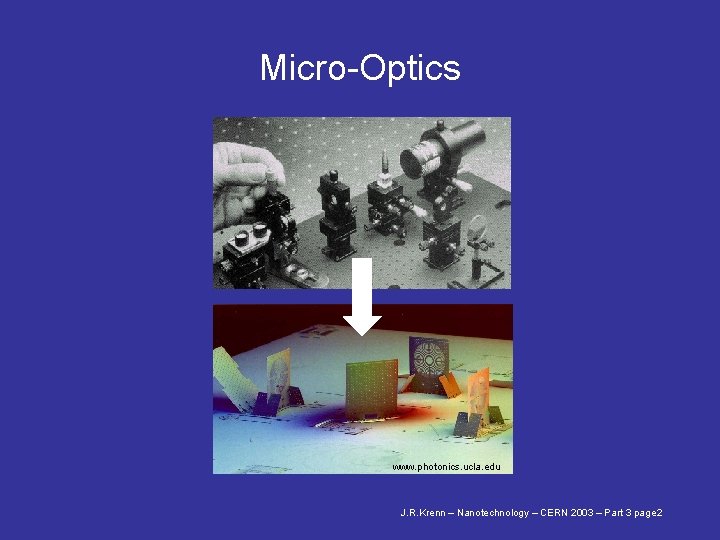
Micro-Optics www. photonics. ucla. edu J. R. Krenn – Nanotechnology – CERN 2003 – Part 3 page 2

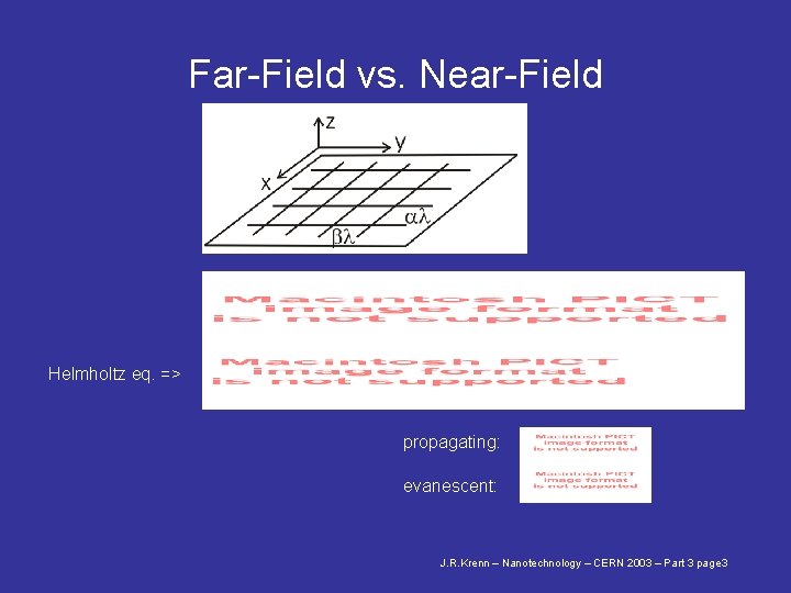
Far-Field vs. Near-Field Helmholtz eq. => propagating: evanescent: J. R. Krenn – Nanotechnology – CERN 2003 – Part 3 page 3

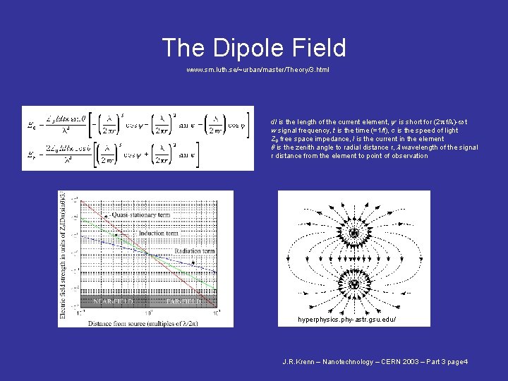
The Dipole Field www. sm. luth. se/~urban/master/Theory/3. html dl is the length of the current element, y is short for (2 p f/l)-w t w signal frequency, t is the time (=1/f), c is the speed of light Z 0 free space impedance, I is the current in the element q is the zenith angle to radial distance r, l wavelength of the signal r distance from the element to point of observation hyperphysics. phy-astr. gsu. edu/ J. R. Krenn – Nanotechnology – CERN 2003 – Part 3 page 4

Near-Field Theory • We have to solve the full set of Maxwell's equations. • Brute force limits applicability due to computing time restrictions. • Complex geometries call for discretization in direct space. • Green's Dyadic Technique, Discrete Dipole Approximation • Finite Difference Time Domain Problems • combining µm-scale structures (e. g. , substrates, waveguides) and nm-structures • including measurement process J. R. Krenn – Nanotechnology – CERN 2003 – Part 3 page 5

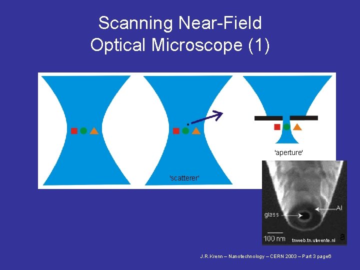
Scanning Near-Field Optical Microscope (1) 'aperture' 'scatterer' tnweb. tn. utwente. nl J. R. Krenn – Nanotechnology – CERN 2003 – Part 3 page 6

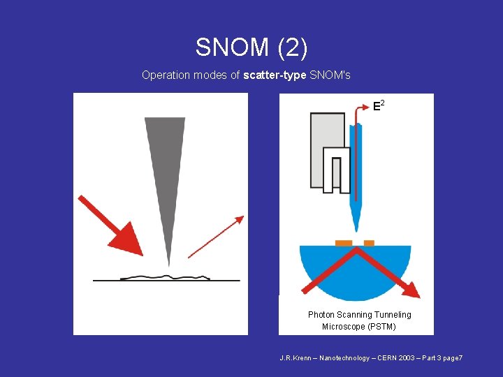
SNOM (2) Operation modes of scatter-type SNOM's E 2 Photon Scanning Tunneling Microscope (PSTM) J. R. Krenn – Nanotechnology – CERN 2003 – Part 3 page 7

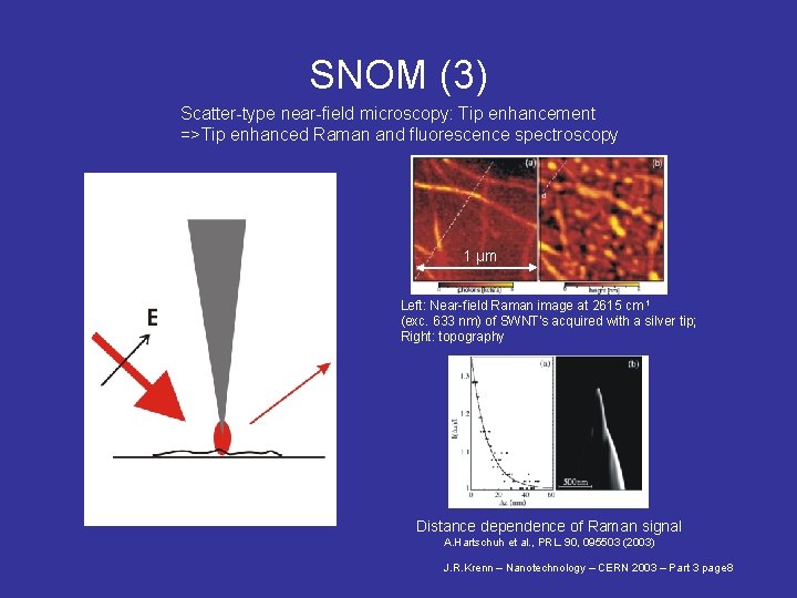
SNOM (3) Scatter-type near-field microscopy: Tip enhancement =>Tip enhanced Raman and fluorescence spectroscopy 1 µm Left: Near-field Raman image at 2615 cm-1 (exc. 633 nm) of SWNT's acquired with a silver tip; Right: topography Distance dependence of Raman signal A. Hartschuh et al. , PRL. 90, 095503 (2003) J. R. Krenn – Nanotechnology – CERN 2003 – Part 3 page 8

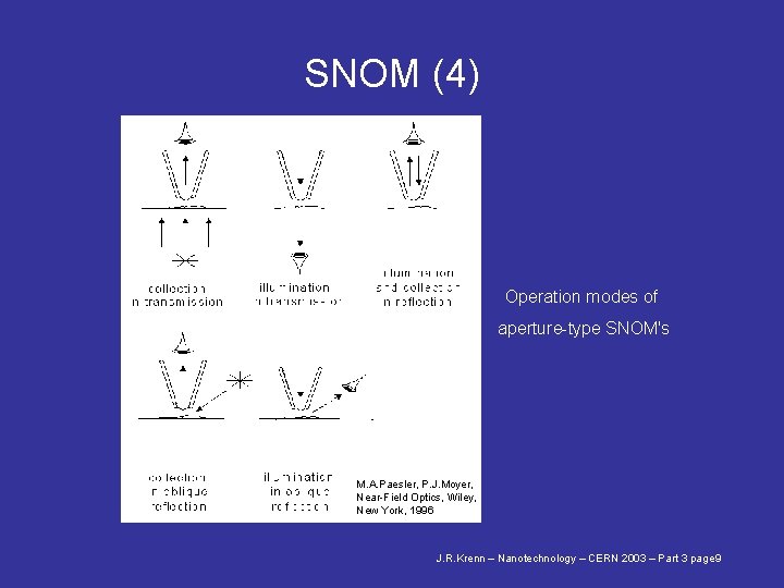
SNOM (4) Operation modes of aperture-type SNOM's illumination M. A. Paesler, P. J. Moyer, in total internal Near-Field Optics, Wiley, New York, 1996 reflection J. R. Krenn – Nanotechnology – CERN 2003 – Part 3 page 9

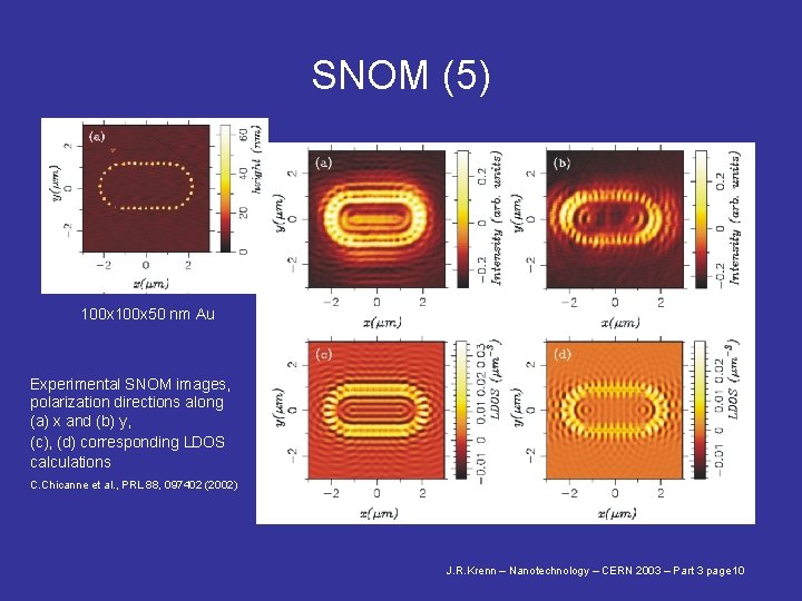
SNOM (5) 100 x 50 nm Au Experimental SNOM images, polarization directions along (a) x and (b) y, (c), (d) corresponding LDOS calculations C. Chicanne et al. , PRL 88, 097402 (2002) J. R. Krenn – Nanotechnology – CERN 2003 – Part 3 page 10

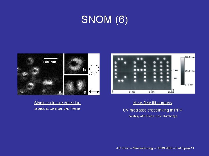
SNOM (6) pol. Single molecule detection Near-field lithography courtesy N. van Hulst, Univ. Twente UV mediated crosslinking in PPV courtesy of R. Riehn, Univ. Cambridge J. R. Krenn – Nanotechnology – CERN 2003 – Part 3 page 11

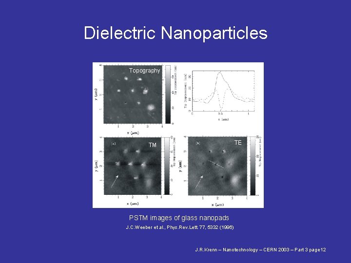
Dielectric Nanoparticles Topography TE TM PSTM images of glass nanopads J. C. Weeber et al. , Phys. Rev. Lett. 77, 5332 (1996) J. R. Krenn – Nanotechnology – CERN 2003 – Part 3 page 12

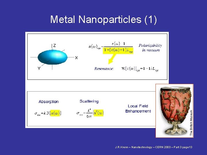
The British Museum Metal Nanoparticles (1) J. R. Krenn – Nanotechnology – CERN 2003 – Part 3 page 13

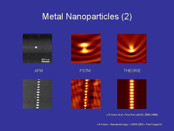
Metal Nanoparticles (2) 500 nm AFM PSTM THEORIE J. R. Krenn et al. , Phys. Rev. Lett. 82, 2590 (1999) J. R. Krenn – Nanotechnology – CERN 2003 – Part 3 page 14

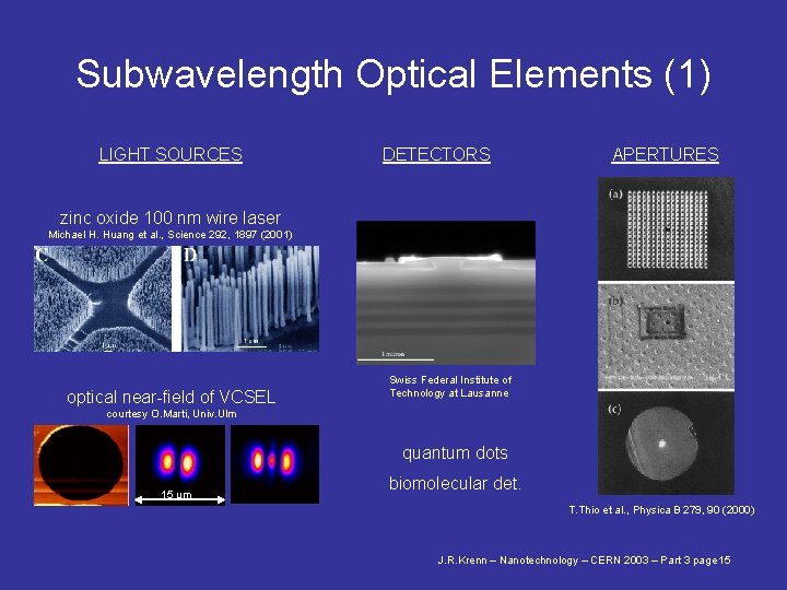
Subwavelength Optical Elements (1) LIGHT SOURCES DETECTORS APERTURES zinc oxide 100 nm wire laser Michael H. Huang et al. , Science 292, 1897 (2001) optical near-field of VCSEL Swiss Federal Institute of Technology at Lausanne courtesy O. Marti, Univ. Ulm quantum dots 15 µm biomolecular det. T. Thio et al. , Physica B 279, 90 (2000) J. R. Krenn – Nanotechnology – CERN 2003 – Part 3 page 15

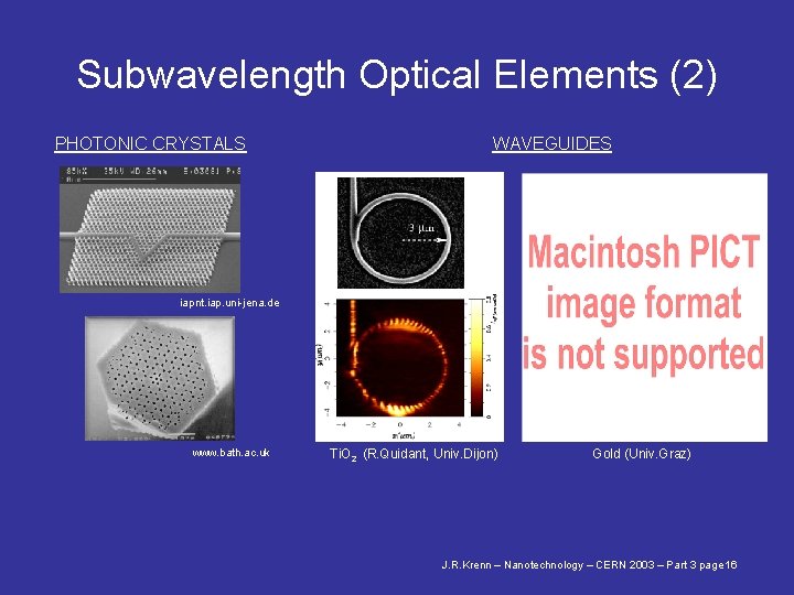
Subwavelength Optical Elements (2) PHOTONIC CRYSTALS WAVEGUIDES iapnt. iap. uni-jena. de www. bath. ac. uk Ti. O 2 (R. Quidant, Univ. Dijon) Gold (Univ. Graz) J. R. Krenn – Nanotechnology – CERN 2003 – Part 3 page 16

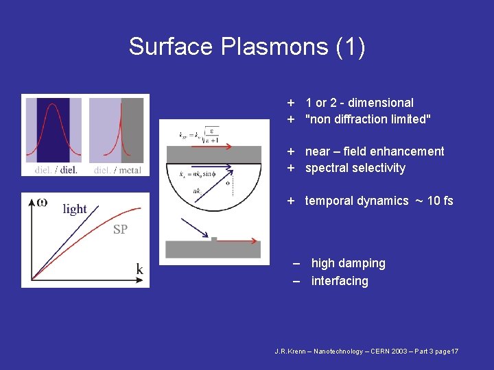
Surface Plasmons (1) + 1 or 2 - dimensional + "non diffraction limited" + near – field enhancement + spectral selectivity + temporal dynamics ~ 10 fs – high damping – interfacing J. R. Krenn – Nanotechnology – CERN 2003 – Part 3 page 17

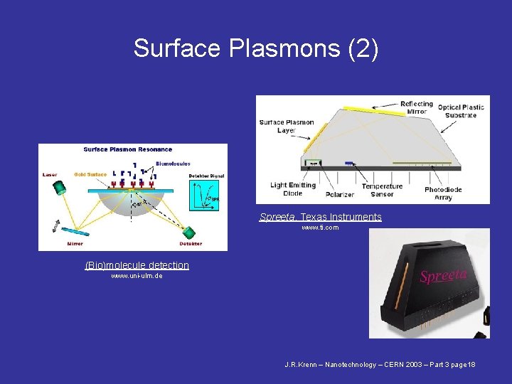
Surface Plasmons (2) Spreeta, Texas Instruments www. ti. com (Bio)molecule detection www. uni-ulm. de J. R. Krenn – Nanotechnology – CERN 2003 – Part 3 page 18

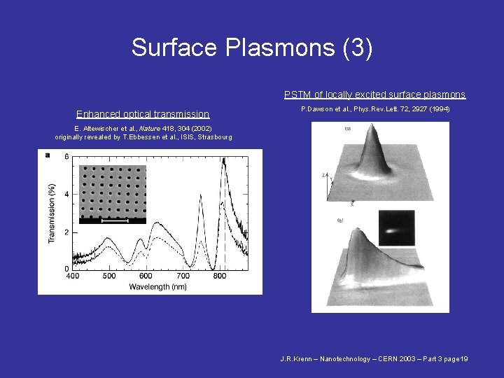
Surface Plasmons (3) PSTM of locally excited surface plasmons Enhanced optical transmission P. Dawson et al. , Phys. Rev. Lett. 72, 2927 (1994) E. Altewischer et al. , Nature 418, 304 (2002) originally revealed by T. Ebbessen et al. , ISIS, Strasbourg J. R. Krenn – Nanotechnology – CERN 2003 – Part 3 page 19

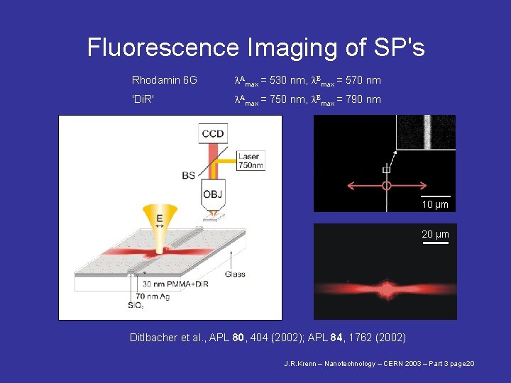
Fluorescence Imaging of SP's Rhodamin 6 G l. Amax = 530 nm, l. Emax = 570 nm 'Di. R' l. Amax = 750 nm, l. Emax = 790 nm 10 µm 20 µm Ditlbacher et al. , APL 80, 404 (2002); APL 84, 1762 (2002) J. R. Krenn – Nanotechnology – CERN 2003 – Part 3 page 20

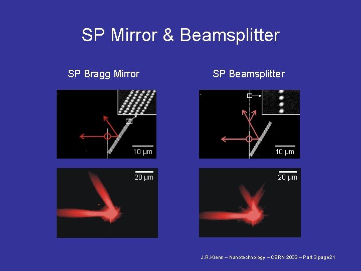
SP Mirror & Beamsplitter SP Bragg Mirror 10 µm 20 µm SP Beamsplitter 10 µm 20 µm J. R. Krenn – Nanotechnology – CERN 2003 – Part 3 page 21

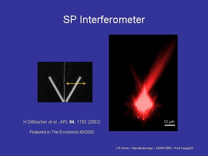
SP Interferometer H. Ditlbacher et al. , APL 84, 1762 (2002) 10 µm Featured in The Economist 43/2002 J. R. Krenn – Nanotechnology – CERN 2003 – Part 3 page 22

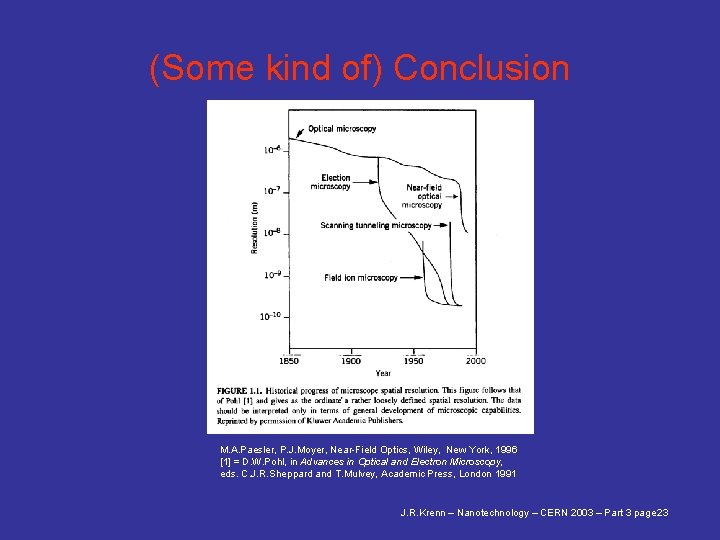
(Some kind of) Conclusion M. A. Paesler, P. J. Moyer, Near-Field Optics, Wiley, New York, 1996 [1] = D. W. Pohl, in Advances in Optical and Electron Microscopy, eds. C. J. R. Sheppard and T. Mulvey, Academic Press, London 1991 J. R. Krenn – Nanotechnology – CERN 2003 – Part 3 page 23