
Nanosystem Fabrication Facility Workshop for Electron Beam Lithography
Nanosystem Fabrication Facility Workshop for Electron Beam Lithography System JBX-6300 FS By Nelson LI 13 November 2009 Page 1
1. System specifications 2. Importance of chip feature on writing result 3. Requirements of overlay writing 4. Photoresist provide 5. Requirements of pattern design 6. Exposure result 7. Charging scheme Page 2
1. System specifications • System model • Basic specifications • Substrates supported by system Page 3
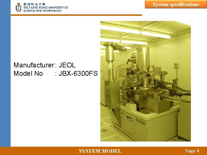
System specifications Manufacturer : JEOL Model No : JBX-6300 FS SYSTEM MODEL Page 4
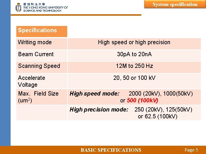
System specification Specifications Writing mode High speed or high precision Beam Current 30 p. A to 20 n. A Scanning Speed 12 M to 250 Hz Accelerate Voltage Max. Field Size (um 2) 20, 50 or 100 k. V High speed mode: 2000 (20 k. V), 1000(50 k. V) or 500 (100 k. V) High precision mode: 250 (20 k. V), 125(50 k. V) or 62. 5 (100 k. V) BASIC SPECIFICATIONS Page 5
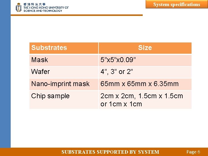
System specifications Substrates Size Mask 5”x 0. 09” Wafer 4”, 3” or 2” Nano-imprint mask 65 mm x 6. 35 mm Chip sample 2 cm x 2 cm, 1. 5 cm x 1. 5 cm or 1 cm x 1 cm SUBSTRATES SUPPORTED BY SYSTEM Page 6
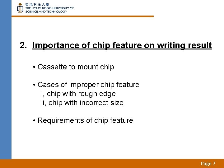
2. Importance of chip feature on writing result • Cassette to mount chip • Cases of improper chip feature i, chip with rough edge ii, chip with incorrect size • Requirements of chip feature Page 7
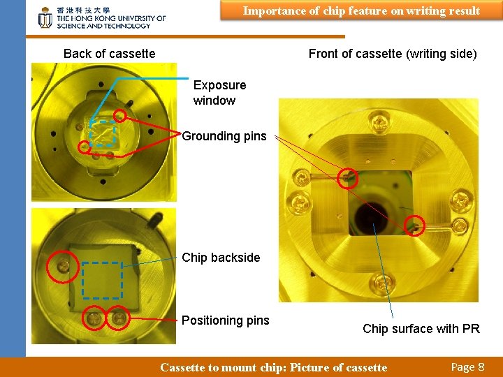
Importance of chip feature on writing result Back of cassette Front of cassette (writing side) Exposure window Grounding pins Chip backside Positioning pins Chip surface with PR Cassette to mount chip: Picture of cassette Page 8
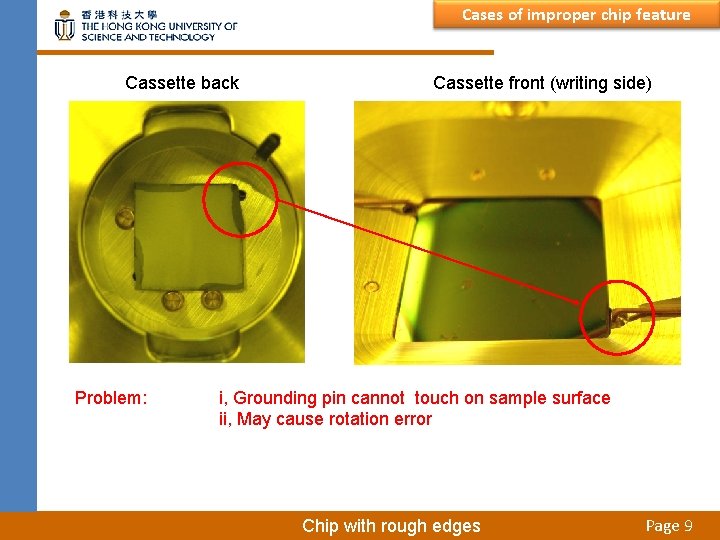
Cases of improper chip feature Cassette back Problem: Cassette front (writing side) i, Grounding pin cannot touch on sample surface ii, May cause rotation error Chip with rough edges Page 9
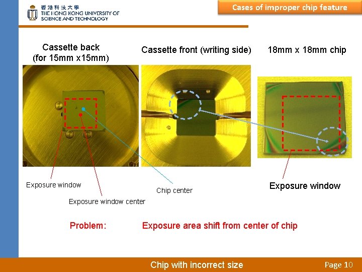
Cases of improper chip feature Cassette back (for 15 mm x 15 mm) chip) Cassette front (writing side) Exposure window Chip center 18 mm x 18 mm chip Exposure window center Problem: Exposure area shift from center of chip Chip with incorrect size Page 10
Importance of chip feature on writing result • Straight and smooth cutting edge • Square shape with orthogonal angles • For overlay writing, patterns of previous layer should be located at the center of chip Requirements of chip feature Page 11
3. Requirements of overlay writing • Feature of Global and Chip alignment marks • Positions of Global and Chip alignment marks Page 12
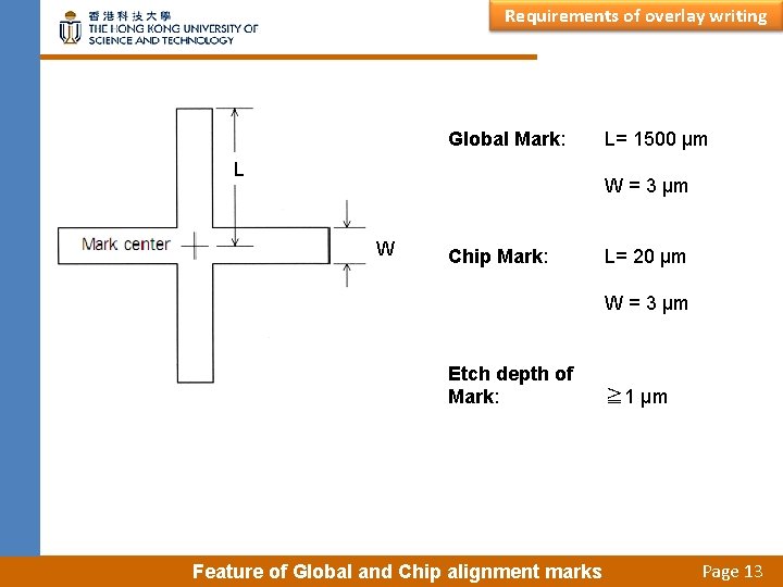
Requirements of overlay writing Global Mark: L L= 1500 μm W = 3 μm W Chip Mark: L= 20 μm W = 3 μm Etch depth of Mark: Feature of Global and Chip alignment marks ≧ 1 μm Page 13
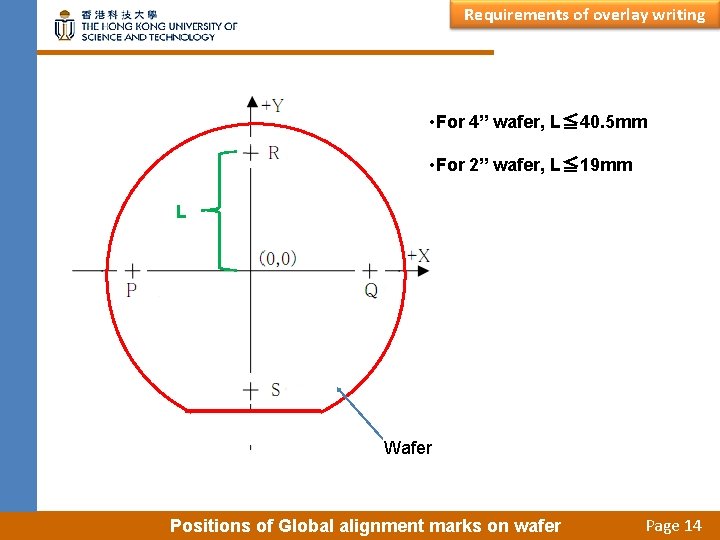
Requirements of overlay writing • For 4” wafer, L≦ 40. 5 mm • For 2” wafer, L≦ 19 mm L Wafer Positions of Global alignment marks on wafer Page 14
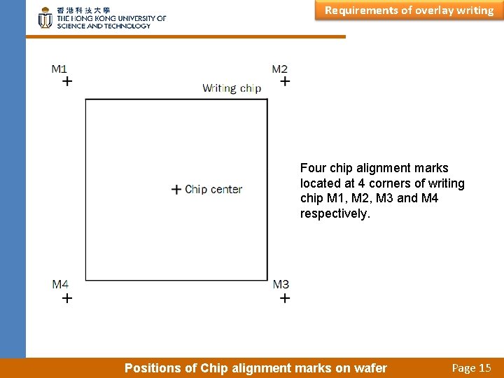
Requirements of overlay writing Four chip alignment marks located at 4 corners of writing chip M 1, M 2, M 3 and M 4 respectively. Positions of Chip alignment marks on wafer Page 15
4. Photoresist Provide • Positive photoresist i, ZEP-520 A (thickness ~ 400 to 100 nm) ii, ZEP-7000 (for mask, thickness ~ 400 to 150 nm) iii, PMMA 950 -A 2 (thickness ~ 180 to 80 nm) • Negative photoresist i, AR-N 7520. 18 (thickness ~ 400 nm) ii, AR-N 7520. 073 (thickness ~ 100 nm) Page 16
5. Requirements of pattern design • File format, pattern sizes and pattern area • Pattern samples Page 17
Requirements of pattern • File format: GDSII • Total number of vertex point per polygon ≦ 600 • Pattern sizes(line width or gap size) ≧ 100 nm • Pattern Complexity ↑, file conversion time ↑ Pattern sizes and file format Page 18
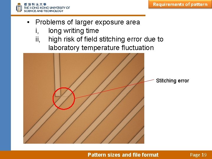
Requirements of pattern • Problems of larger exposure area i, long writing time ii, high risk of field stitching error due to laboratory temperature fluctuation Stitching error Pattern sizes and file format Page 19
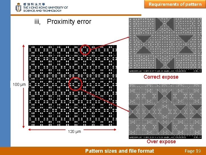
Requirements of pattern iii, Proximity error Correct expose 100 μm 120 μm Over expose Pattern sizes and file format Page 19
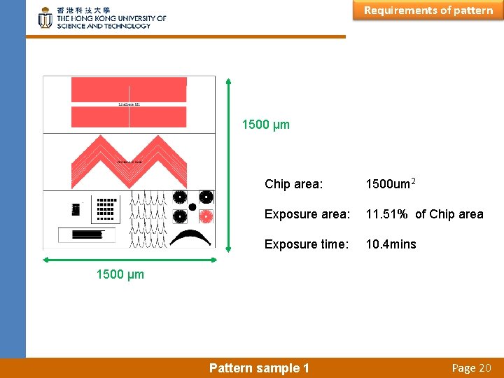
Requirements of pattern 1500 μm Chip area: 1500 um 2 Exposure area: 11. 51% of Chip area Exposure time: 10. 4 mins 1500 μm Pattern sample 1 Page 20
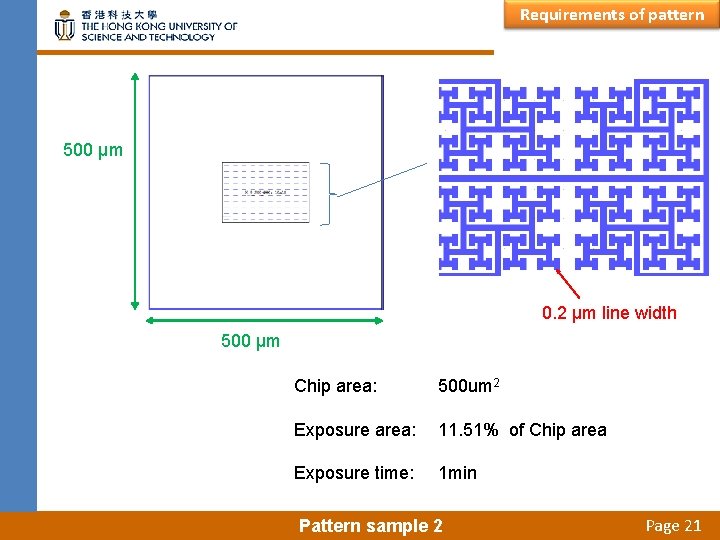
Requirements of pattern 500 μm 0. 2 μm line width 500 μm Chip area: 500 um 2 Exposure area: 11. 51% of Chip area Exposure time: 1 min Pattern sample 2 Page 21
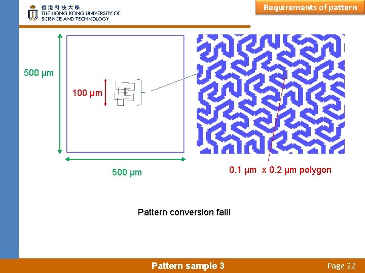
Requirements of pattern 500 μm 100 μm 0. 1 μm x 0. 2 μm polygon 500 μm Pattern conversion fail! Pattern sample 3 Page 22
6. Exposure result • Pattern sample 1 • Pattern sample 2 Page 23
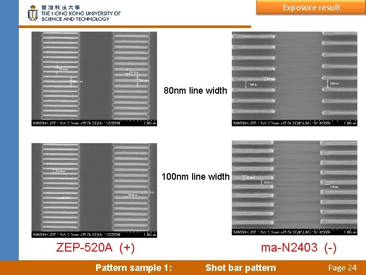
Exposure result 80 nm line width 100 nm line width ZEP-520 A (+) Pattern sample 1: ma-N 2403 (-) Shot bar pattern Page 24
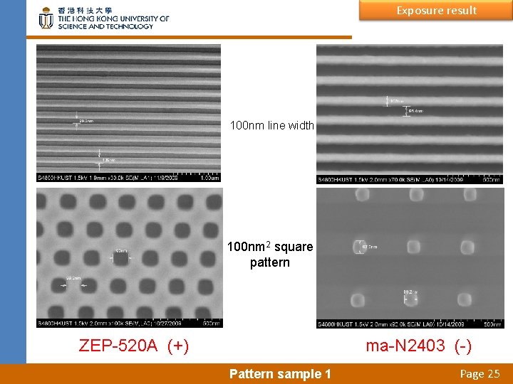
Exposure result 100 nm line width 100 nm 2 square pattern ZEP-520 A (+) ma-N 2403 (-) Pattern sample 1 Page 25
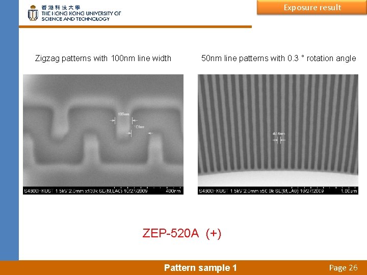
Exposure result Zigzag patterns with 100 nm line width 50 nm line patterns with 0. 3 ° rotation angle ZEP-520 A (+) Pattern sample 1 Page 26
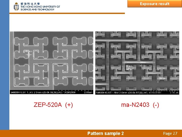
Exposure result ZEP-520 A (+) ma-N 2403 (-) Pattern sample 2 Page 27
7. Charging Scheme • Definitions of Short and Long jobs • Charging for internal users • Charging for other HK Institutions • Charging for external users • Job submission procedure Page 28
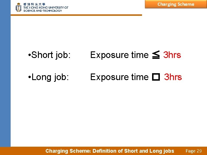
Charging Scheme • Short job: Exposure time ≦ 3 hrs • Long job: Exposure time � 3 hrs Charging Scheme: Definition of Short and Long jobs Page 29
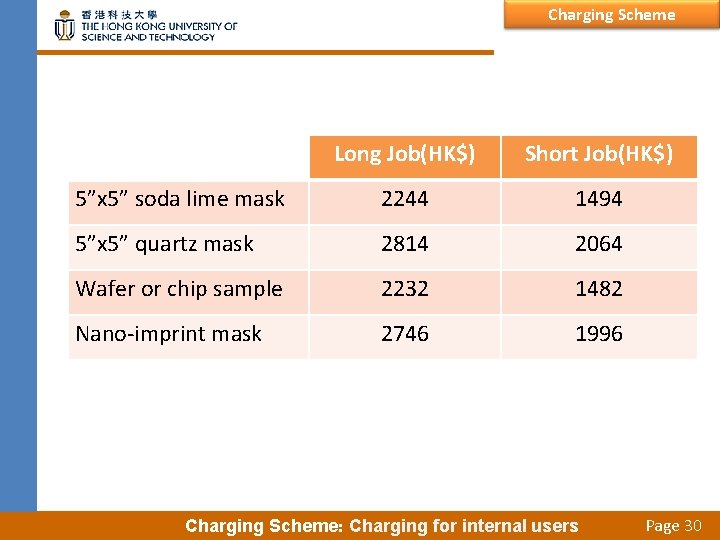
Charging Scheme Long Job(HK$) Short Job(HK$) 5”x 5” soda lime mask 2244 1494 5”x 5” quartz mask 2814 2064 Wafer or chip sample 2232 1482 Nano-imprint mask 2746 1996 Charging Scheme: Charging for internal users Page 30
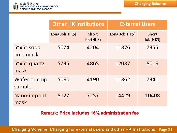
Charging Scheme Other HK Institutions External Users Long Job(HK$) Short Job(HK$) 5”x 5” soda lime mask 5074 4204 11376 7355 5”x 5” quartz mask 5735 4865 12037 8016 Wafer or chip sample 5060 4190 11362 7341 Nano-imprint mask 8127 7257 14429 10408 Remark: Price includes 16% administration fee Charging Scheme: Charging for external users and other HK Institutions Page 31
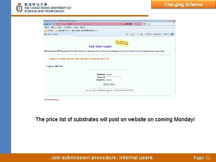
Charging Scheme The price list of substrates will post on website on coming Monday! Job submission procedure: internal users Page 32
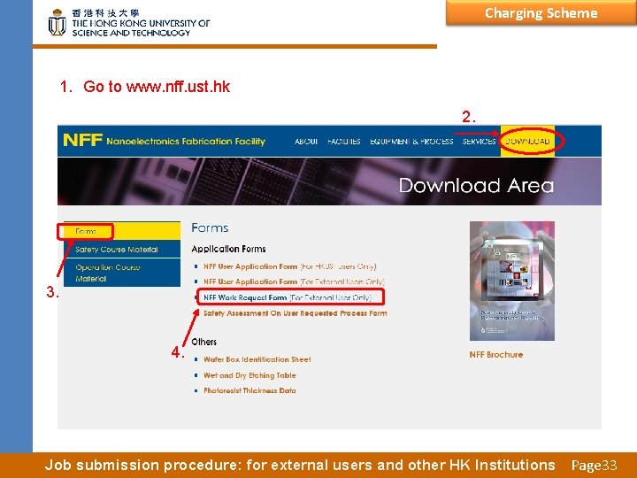
Charging Scheme 1. Go to www. nff. ust. hk 2. 3. 4. Job submission procedure: for external users and other HK Institutions Page 33
Nanoelectronics Fabrication Facility Thankyou Contact Information : Name: Nelson LI Email : eenelson@ust. hk Job submission procedure Page 34
- Slides: 35