NANOSCALE LITHOGRAPHY MICHAEL JOHNSTON 4132015 ABSTRACT AND OUTLINE

NANOSCALE LITHOGRAPHY MICHAEL JOHNSTON 4/13/2015

ABSTRACT AND OUTLINE • Nanoscale Lithography is an ever growing fabrication process due to technology demands. We are continuously striving to increase the number of transistors on a chip to increase performance. The drive for smaller and faster technologies has caused the development of fabrication techniques that allow us to work at the nanoscale feature size. A few lithography techniques will be explored to show this whole process works. The processes I will cover include Photo, Electron Beam and X-Ray lithography. These forms of lithography share a common process of preparation exposure and development while fabricating wafers. • Key Terms: Photolithography, Electron Beam Lithography, X-Ray Lithography, Photo Resist, Electron Scattering, Photo Mask, Ionization • Overview(What, Why, Nano) • Photolithography • Electron Beam Lithography • X-Ray Lithography • Conclusion • References • Concept Check

WHAT IS LITHOGRAPHY!? • The process of transferring or printing a pattern from one medium to another • Johann Alois Senefelder (1796), used ink on limestone

TECHNOLOGY TRENDS • Moore’s Law • Smaller, Faster, Cheaper • Performance

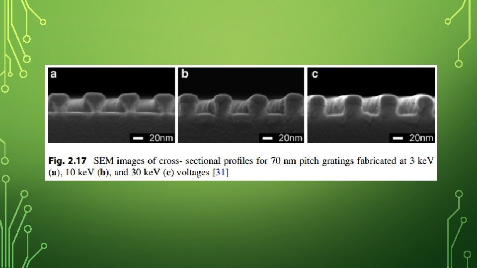
NANOSCALE LITHOGRAPHY • Using Lithographic tools for fabrication of any structures having feature size of less than 100 nm • Human hair is ~80, 000 nm thick • Downscale feature size, high throughput and quality

FORMS OF LITHOGRAPHY • Photo • Electron Beam • X-Ray • Projection Printing • Direct Writing • Proximity Printing

PHOTOLITHOGRAPHY • UV light passes through focusing lenses and masks to react with a photoresist to form patterns on a wafer • Projection Printing Technique • Limited by diffraction limit

PHOTOLITHOGRAPHY PROCESS • General Steps: 1. Substrate preparation 2. Photoresist 3. Alignment and Masking 4. Development

PHOTOLITHOGRAPHY PROCESS 1. SUBSTRATE PREPARATION • Use modern clean rooms with robotic wafer cleaning systems • Surface Impurities are removed by wet chemical treatment • Baked to remove moisture 2. PHOTORESIST • Apply a layer of resist that will react to the light • Evenly coated by spin coating

PHOTOLITHOGRAPHY PROCESS ALIGNMENT AND MASKING • Wafer is carefully aligned using automated mechanical process • Mask is aligned over wafer with desired pattern DEVELOPMENT • Developed using liquid solvent • Wet or Dry Etching performed on substrate • Photo Resist strip
 • Highly focused electron beam is • Nanoscale design is")
ELECTRON BEAM LITHOGRAPHY (EBL) • Highly focused electron beam is • Nanoscale design is done on exposed to a resist material that modifies the solubility of the resist for development computers and the pattern is written on a chip using highly precise mechanical devices • Allows accuracy down to as • Goals of EBL writing are highly small as 10 nm dimensions accurate and reliable pattern writing

LIMITING FACTORS IN EBL • Quality of the Electron Optics • Choice of Substrate, Resist, Developer • Electron Beam Energy Level and Dose • Development Time and Temperature • Electron Scattering

ELECTRON SCATTERING • Mutual repulsive forces from the electrons charges-worse at higher currents and lower energy levels • Gas Scattering-reduced by using a vacuum • Forward and Back Scattering • Ionization (Secondary Electron Generation)

ELECTRON SCATTERING • Forward Scattering- electrons entering resist undergo low energy inelastic collisions which deflect the electrons slightly causing the beam to widen • Back Scattering-electrons pass through the resist into substrate and undergo enough collisions to deflect and reemerge into the resist causing proximity issues

EBL RESISTS • Positive Resist: Converts from low to high solubility when exposed to electrons • PMMA (poly-methyl methacrylate)-longer polymer chain which is broken up into smaller more soluble chains • Negative Resist: Converts to low solubility when exposed to electron beam • HSQ (hydrogen silsesquioxane)undergoes polymer cross-linking to form longer less soluble chains

DEVELOPMENT • After exposure, resist is immersed in a liquid solvent to dissolve the fragments (positive) or non crosslinked molecules (negative). • Temperature and duration are a large factor here • Cold treat PMMA for higher resolution

EBL PROCESS PARAMETERS

ELECTRON ENERGY LEVEL • Inelastic cross sectional area • Electrons with higher energy decreases proportionately to electron energy increasing levels undergo less forward scattering, resulting in a narrower electron beam • In positive resists this causes fewer chain scissions per electron resulting in a lower sensitivity • Higher energy electrons penetrate deeper into the substrate causing proximity issues

X-RAY LITHOGRAPHY • Parallel Proximity Printing • X-Ray lithography uses ultra thin masks ( <2 micro) • X-Rays pass directly through mask and onto wafer • Shorter wavelength than UV (0. 4 -4 nm)

CHALLENGES OF X-RAY LITHOGRAPHY • The thin masks are prone to deform due to small stresses • Masks deformation is huge in XRL because of the direct mapping • X-Rays cannot be focused through a lens

CONCLUSION PHOTO ELECTRON BEAM X-RAY UV Light Direct Writing Proximity Printing Limited by UV Wavelength Expensive Efficient Projection Printing Highly Accurate Low Throughput Expensive/Fragile Masks Primarily Used to develop masks for X -Ray

REFERENCES • Stepanova, Maria, and Steven Dew. Nanofabrication: Techniques and Principles. Wien: Springer. Wien. New. York, 2012. Print. • • Jackson, M. J. "Microfabrication Using X-Ray Lithography" Micro and Nanomanufacturing Springer, 2007. Print. • • • Pictures: H. J. Levinson, Principles of Lithography, Second Edition, SPIE Press, Bellingham, WA (2005). Available at: http: //spie. org/x 33182. xml “Senefelder” http: //en. wikipedia. org/wiki/Alois_Senefelder#/media/File: Senefelder. jpg “Moore’s Law” http: //www. cuug. ab. ca/~branderr/eeepc/016_moores_law_intel. html “Hair” http: //waynesword. palomar. edu/lmexer 1. htm “E-Beam Lithography” http: //www. ece. umd. edu/class/enee 416/Group. Activities/Ebeam. pdf

CONCEPT CHECK • Describe the basic lithographic process • What types of resist are used, and what are the differences between them? • What are three lithographic processes and what type of printing do they perform? • What is forward and back scattering and how do they effect the fabrication process? • What is a drawback of EBL?
- Slides: 24