Nanomaterials and Nanostructures Introduction Economy of promises Hype





![Invention of Titania Nano-fibers § Process Adv. Matls. , 16[3], 260 (2004) Patent appl. Invention of Titania Nano-fibers § Process Adv. Matls. , 16[3], 260 (2004) Patent appl.](https://slidetodoc.com/presentation_image/a5d50c64b2f619f9ed26daf5afe92ba2/image-29.jpg)

- Slides: 36

Nano-materials and Nano-structures - Introduction Economy of promises! Hype? Can nanotechnology cure cancer by 2015? Or Real? GETTY Most people learn about developments in science and medicine from the mass media.

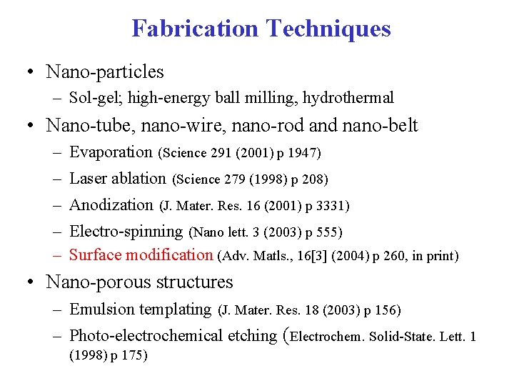
Fabrication Techniques • Nano-particles – Sol-gel; high-energy ball milling, hydrothermal • Nano-tube, nano-wire, nano-rod and nano-belt – Evaporation (Science 291 (2001) p 1947) – Laser ablation (Science 279 (1998) p 208) – Anodization (J. Mater. Res. 16 (2001) p 3331) – Electro-spinning (Nano lett. 3 (2003) p 555) – Surface modification (Adv. Matls. , 16[3] (2004) p 260, in print) • Nano-porous structures – Emulsion templating (J. Mater. Res. 18 (2003) p 156) – Photo-electrochemical etching (Electrochem. Solid-State. Lett. 1 (1998) p 175)

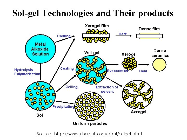
Sol-gel Technologies and Their products Xerogel film Heat Coating Metal Alkoxide Solution Hydrolysis Polymerization Dense film Wet gel Coating Gelling Dense ceramics Xerogel Evaporation Heat Extraction of solvent Precipitating Aerogel Sol Uniform particles Source: http: //www. chemat. com/html/solgel. html

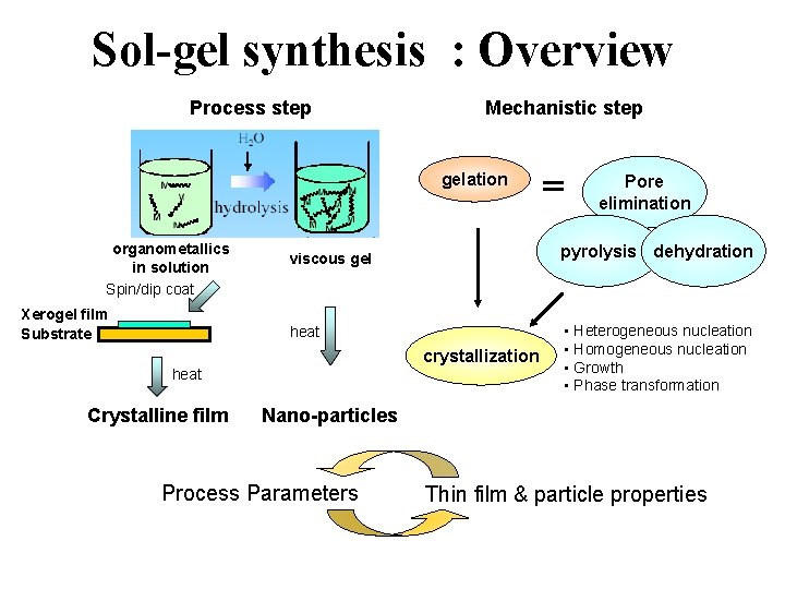
Sol-gel synthesis : Overview Process step Mechanistic step gelation organometallics in solution Spin/dip coat Xerogel film Substrate pyrolysis dehydration viscous gel heat crystallization heat Crystalline film Pore elimination • Heterogeneous nucleation • Homogeneous nucleation • Growth • Phase transformation Nano-particles Process Parameters Thin film & particle properties

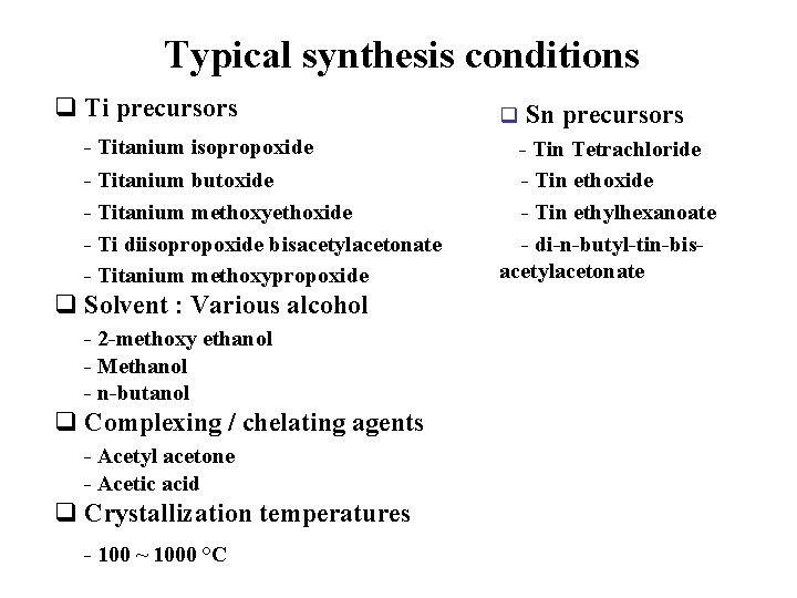
Typical synthesis conditions q Ti precursors - Titanium isopropoxide - Titanium butoxide - Titanium methoxyethoxide - Ti diisopropoxide bisacetylacetonate - Titanium methoxypropoxide q Solvent : Various alcohol - 2 -methoxy ethanol - Methanol - n-butanol q Complexing / chelating agents - Acetyl acetone - Acetic acid q Crystallization temperatures - 100 ~ 1000 °C q Sn precursors - Tin Tetrachloride - Tin ethoxide - Tin ethylhexanoate - di-n-butyl-tin-bisacetylacetonate

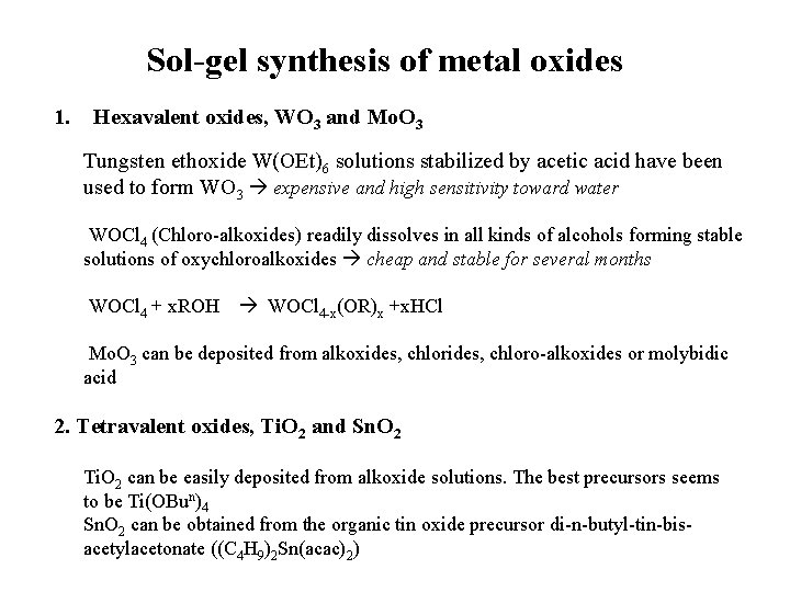
Sol-gel synthesis of metal oxides 1. Hexavalent oxides, WO 3 and Mo. O 3 Tungsten ethoxide W(OEt)6 solutions stabilized by acetic acid have been used to form WO 3 expensive and high sensitivity toward water WOCl 4 (Chloro-alkoxides) readily dissolves in all kinds of alcohols forming stable solutions of oxychloroalkoxides cheap and stable for several months WOCl 4 + x. ROH WOCl 4 -x(OR)x +x. HCl Mo. O 3 can be deposited from alkoxides, chloro-alkoxides or molybidic acid 2. Tetravalent oxides, Ti. O 2 and Sn. O 2 Ti. O 2 can be easily deposited from alkoxide solutions. The best precursors seems to be Ti(OBun)4 Sn. O 2 can be obtained from the organic tin oxide precursor di-n-butyl-tin-bisacetylacetonate ((C 4 H 9)2 Sn(acac)2)

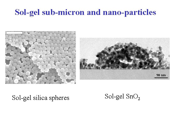
Sol-gel sub-micron and nano-particles Sol-gel silica spheres Sol-gel Sn. O 2

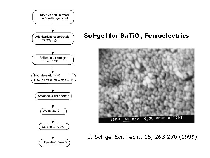
Sol-gel for Ba. Ti. O 3 Ferroelectrics J. Sol-gel Sci. Tech. , 15, 263 -270 (1999)

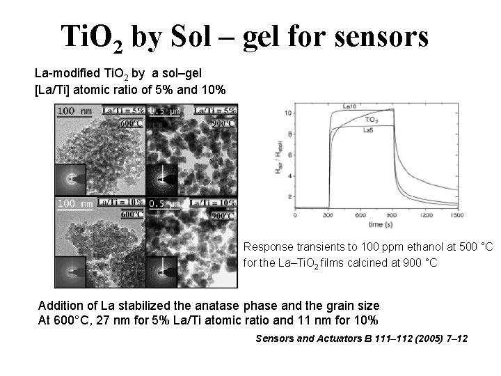
Ti. O 2 by Sol – gel for sensors La-modified Ti. O 2 by a sol–gel [La/Ti] atomic ratio of 5% and 10% Response transients to 100 ppm ethanol at 500 °C for the La–Ti. O 2 films calcined at 900 °C Addition of La stabilized the anatase phase and the grain size At 600°C, 27 nm for 5% La/Ti atomic ratio and 11 nm for 10% Sensors and Actuators B 111– 112 (2005) 7– 12

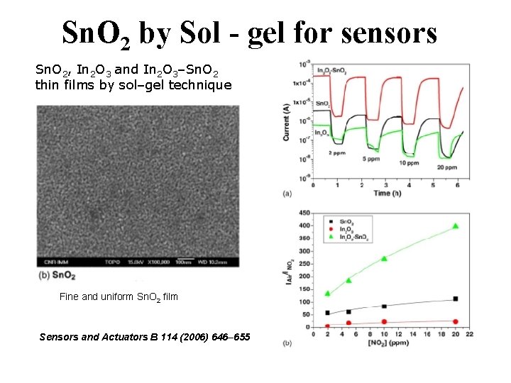
Sn. O 2 by Sol - gel for sensors Sn. O 2, In 2 O 3 and In 2 O 3–Sn. O 2 thin films by sol–gel technique Fine and uniform Sn. O 2 film Sensors and Actuators B 114 (2006) 646– 655

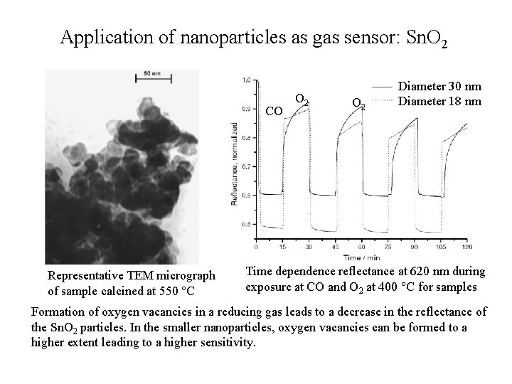
Application of nanoparticles as gas sensor: Sn. O 2 CO Representative TEM micrograph of sample calcined at 550 C O 2 Diameter 30 nm Diameter 18 nm Time dependence reflectance at 620 nm during exposure at CO and O 2 at 400 C for samples Formation of oxygen vacancies in a reducing gas leads to a decrease in the reflectance of the Sn. O 2 particles. In the smaller nanoparticles, oxygen vacancies can be formed to a higher extent leading to a higher sensitivity.

General Conclusion of Sol - gel ØVersatile powders, films, fibers, monoliths, aerogels, xerogels ØHigh purity controlled by purity of starting solution ØHomogeneity controlled by hydrolysis, condensation and polymerization reactions ØLimited mass-scale production particles, coatings, thin-films

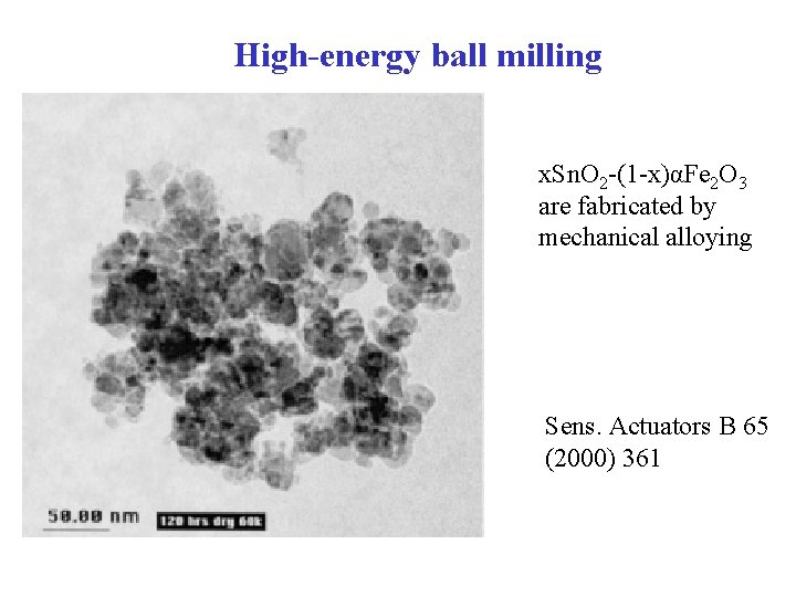
High-energy ball milling x. Sn. O 2 -(1 -x)αFe 2 O 3 are fabricated by mechanical alloying Sens. Actuators B 65 (2000) 361

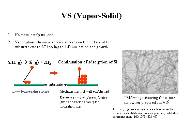
VS (Vapor-Solid) 1. No metal catalysts used 2. Vapor phase chemical species adsorbs on the surface of the substrate due to DT leading to 1 -D nucleation and growth Si. H 4(g) Si (g) + 2 H 2 Continuation of adsorption of Si substrate Low temperature zone Mechanism is not well established Screw dislocation (Sears), Defect (twins or stacking fault) for nucleation sites TEM image showing the silicon nanowires prepared via VS 2 2 P. P. Yu, Synthesis of nano-scale silicon wires by excimer laser ablation at high temperature, Solid state communication, 105(1998) 403 -407.

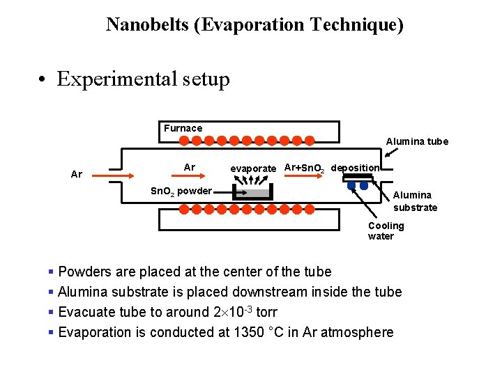
Nanobelts (Evaporation Technique) • Experimental setup Furnace Alumina tube Ar Ar Sn. O 2 powder evaporate Ar+Sn. O 2 deposition Alumina substrate Cooling water § Powders are placed at the center of the tube § Alumina substrate is placed downstream inside the tube § Evacuate tube to around 2 10 -3 torr § Evaporation is conducted at 1350 °C in Ar atmosphere

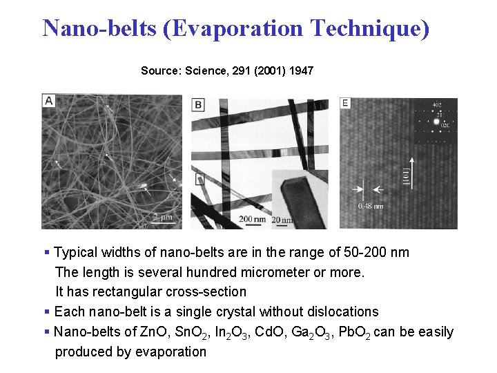
Nano-belts (Evaporation Technique) Source: Science, 291 (2001) 1947 § Typical widths of nano-belts are in the range of 50 -200 nm The length is several hundred micrometer or more. It has rectangular cross-section § Each nano-belt is a single crystal without dislocations § Nano-belts of Zn. O, Sn. O 2, In 2 O 3, Cd. O, Ga 2 O 3, Pb. O 2 can be easily produced by evaporation

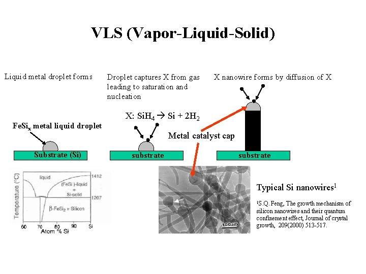
VLS (Vapor-Liquid-Solid) Liquid metal droplet forms Fe. Six metal liquid droplet Substrate (Si) Droplet captures X from gas leading to saturation and nucleation X nanowire forms by diffusion of X X: Si. H 4 Si + 2 H 2 Metal catalyst cap substrate Typical Si nanowires 1 1 S. Q. Feng, The growth mechanism of silicon nanowires and their quantum confinement effect, Journal of crystal growth, 209(2000) 513 -517.


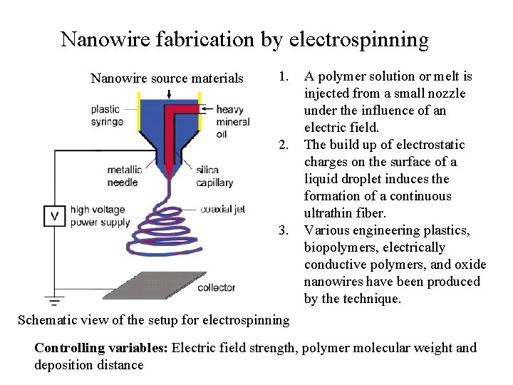
Nanowire fabrication by electrospinning Nanowire source materials 1. 2. 3. A polymer solution or melt is injected from a small nozzle under the influence of an electric field. The build up of electrostatic charges on the surface of a liquid droplet induces the formation of a continuous ultrathin fiber. Various engineering plastics, biopolymers, electrically conductive polymers, and oxide nanowires have been produced by the technique. Schematic view of the setup for electrospinning Controlling variables: Electric field strength, polymer molecular weight and deposition distance

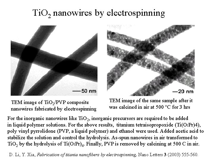
Ti. O 2 nanowires by electrospinning TEM image of Ti. O 2/PVP composite nanowires fabricated by electrospinning TEM image of the sample after it was calcined in air at 500 C for 3 hrs For the inorganic nanowires like Ti. O 2, inorganic precursors are required to be added in liquid polymer solutions. For the above results, titanium tetraisopropoxide (Ti(Oi. Pr)4), poly vinyl pyrrolidone (PVP, a liquid polymer) and ethanol were used. Added acetic acid to stabilize the solution and control the hydrolysis. As-spun nanowires in air transformed to Ti. O 2 by the hydrolysis of Ti(Oi. Pr)4. Finally, PVP is removed by calcining at 500 C in air. D. Li, Y. Xia, Fabrication of titania nanofibers by electrospinning, Nano Letters 3 (2003) 555 -560.

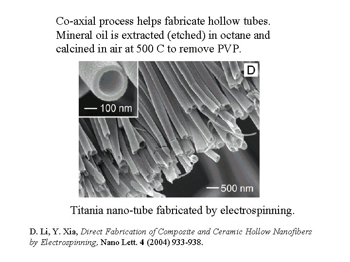
Co-axial process helps fabricate hollow tubes. Mineral oil is extracted (etched) in octane and calcined in air at 500 C to remove PVP. Titania nano-tube fabricated by electrospinning. D. Li, Y. Xia, Direct Fabrication of Composite and Ceramic Hollow Nanofibers by Electrospinning, Nano Lett. 4 (2004) 933 -938.

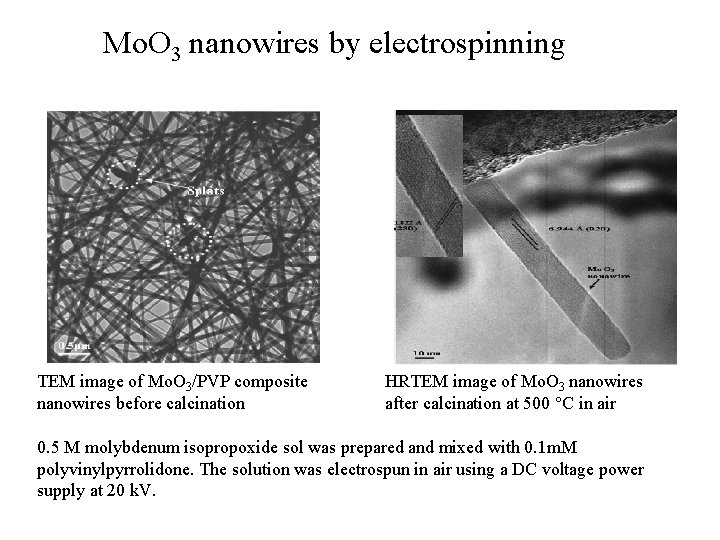
Mo. O 3 nanowires by electrospinning TEM image of Mo. O 3/PVP composite nanowires before calcination HRTEM image of Mo. O 3 nanowires after calcination at 500 C in air 0. 5 M molybdenum isopropoxide sol was prepared and mixed with 0. 1 m. M polyvinylpyrrolidone. The solution was electrospun in air using a DC voltage power supply at 20 k. V.


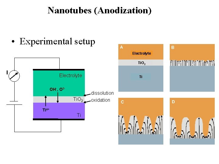
Nanotubes (Anodization) • Experimental setup Electrolyte Ti. O 2 I Electrolyte OH-, O 2 - Ti. O 2 Ti 4+ Ti Ti dissolution oxidation

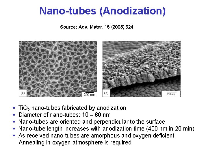
Nano-tubes (Anodization) Source: Adv. Mater. 15 (2003) 624 § § § Ti. O 2 nano-tubes fabricated by anodization Diameter of nano-tubes: 10 – 80 nm Nano-tubes are oriented and perpendicular to the surface Nano-tube length increases with anodization time (400 nm in 20 min) As-received nano-tubes are amorphous and oxygen deficient Annealing in oxygen atmosphere is required

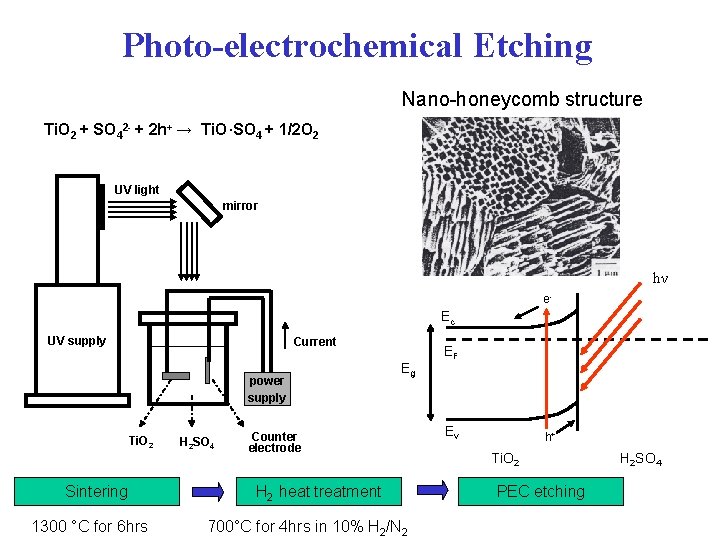
Photo-electrochemical Etching Nano-honeycomb structure Ti. O 2 + SO 42 - + 2 h+ → Ti. O·SO 4 + 1/2 O 2 UV light mirror hν e- Ec UV supply Current power supply Ti. O 2 Sintering 1300 °C for 6 hrs H 2 SO 4 Eg Counter electrode H 2 heat treatment 700°C for 4 hrs in 10% H 2/N 2 EF Ev h+ Ti. O 2 PEC etching H 2 SO 4
![Invention of Titania Nanofibers Process Adv Matls 163 260 2004 Patent appl Invention of Titania Nano-fibers § Process Adv. Matls. , 16[3], 260 (2004) Patent appl.](https://slidetodoc.com/presentation_image/a5d50c64b2f619f9ed26daf5afe92ba2/image-29.jpg)
Invention of Titania Nano-fibers § Process Adv. Matls. , 16[3], 260 (2004) Patent appl. 2003 -678772 Sintering H 2 heat treatment 1200 °C for 6 hrs 700°C for 8 hrs in 5% H 2/N 2 heat-treatment 1 μm - Nano-fibers are parallel, oriented in the same direction - Diameter of nano-fibers: 15 – 50 nm Length of nano-fibers: up to 5 μm

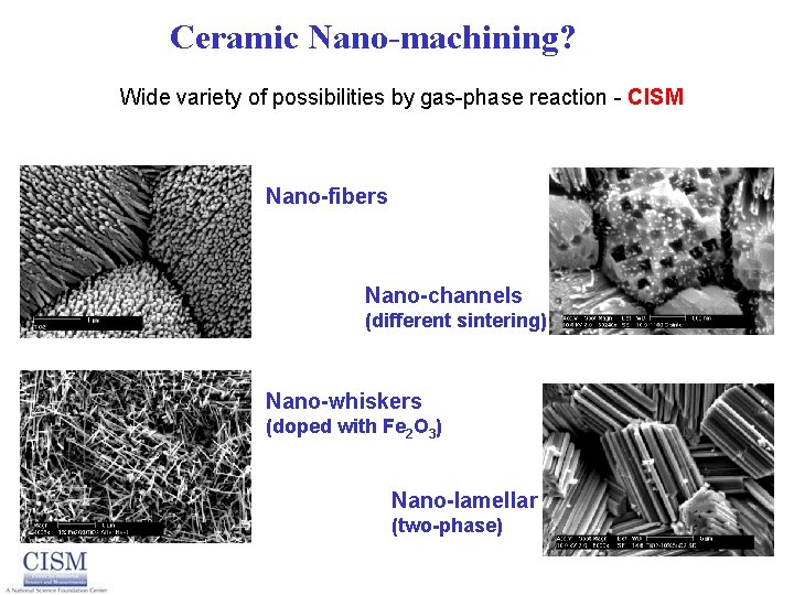
Ceramic Nano-machining? Wide variety of possibilities by gas-phase reaction - CISM Nano-fibers Nano-channels (different sintering) Nano-whiskers (doped with Fe 2 O 3) Nano-lamellar (two-phase)

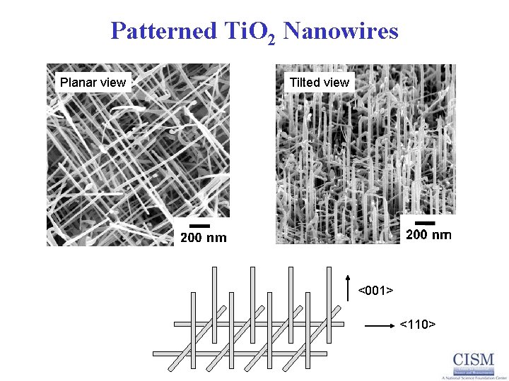
Patterned Ti. O 2 Nanowires Planar view Tilted view <001> <110>

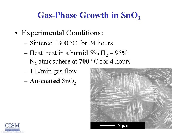
Gas-Phase Growth in Sn. O 2 • Experimental Conditions: – Sintered 1300 C for 24 hours – Heat treat in a humid 5% H 2 – 95% N 2 atmosphere at 700 C for 4 hours – 1 L/min gas flow – Au-coated Sn. O 2 2 m

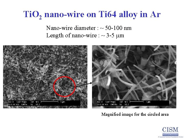
Ti. O 2 nano-wire on Ti 64 alloy in Ar Nano-wire diameter : ~ 50 -100 nm Length of nano-wire : ~ 3 -5 m Magnified image for the circled area

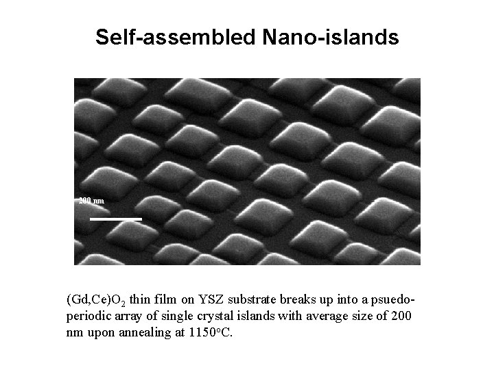
Self-assembled Nano-islands 200 nm (Gd, Ce)O 2 thin film on YSZ substrate breaks up into a psuedoperiodic array of single crystal islands with average size of 200 nm upon annealing at 1150 o. C.

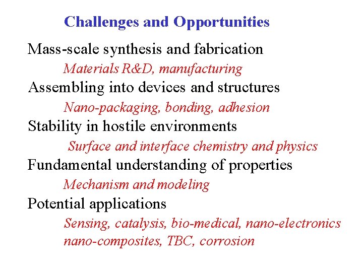
Challenges and Opportunities Mass-scale synthesis and fabrication Materials R&D, manufacturing Assembling into devices and structures Nano-packaging, bonding, adhesion Stability in hostile environments Surface and interface chemistry and physics Fundamental understanding of properties Mechanism and modeling Potential applications Sensing, catalysis, bio-medical, nano-electronics nano-composites, TBC, corrosion

Success Code: RTDAD • Read • Think • Discuss • Ask • Do