Nanolitografi Ebeam litografi Nano imprint litografi Mikroskopi SEM

Nanolitografi E-beam litografi Nano imprint litografi

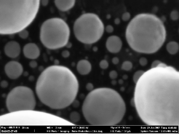
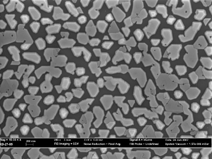
Mikroskopi
")
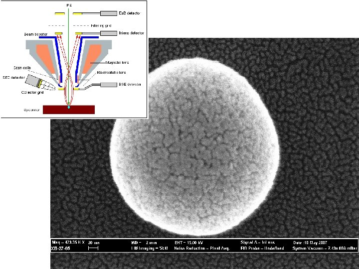
SEM (scanning electron microscope)

Komponenter i SEM Schottky emitter elektronkilde F =-e v x B Magnetisk linse

E-beam litografi - Dedikerede e-beam systemer - SEM med Raith Gmbh kontrolsystem og ’pattern generator’ DANCHIP
")
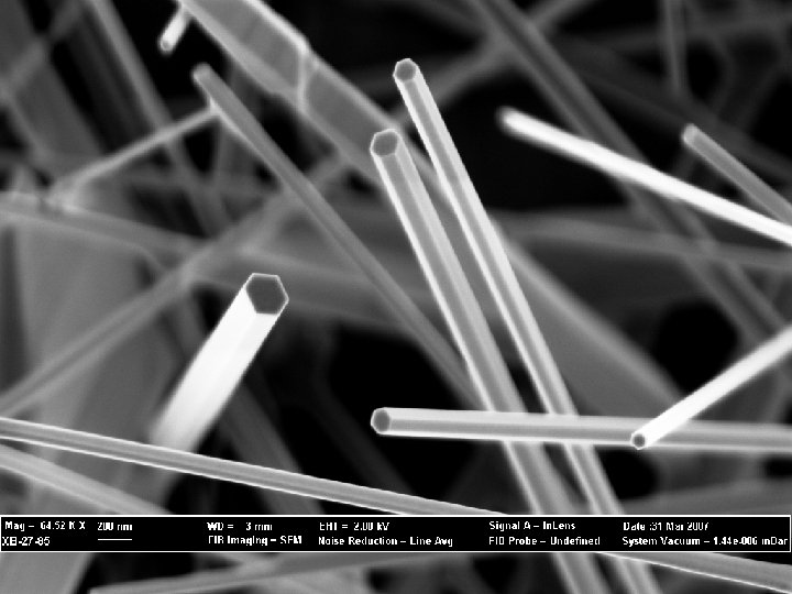
Test of nanowire writing E-beam writing+RIE (Nano 9 – Tom+Jeppe)

Wires and channels

Optiske strukturer Diffraktive komponenter 2 D grating: Periodicity - 250 nm
")
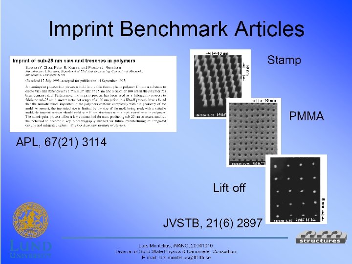
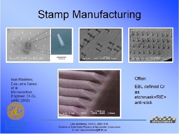
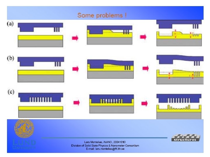
Nano Imprint Lithography (NIL)
")
Nanowire detektor Appl. Phys. Lett. 89, 153102 (2006)
 System")
Focused Ion Beam (FIB) System
")
Focused Ion Beam Writing As the diagram on the right shows, the gallium (Ga+) primary ion beam hits the sample surface and sputters a small amount of material, which leaves the surface as either secondary ions (i+ or i-) or neutral atoms (n 0). The primary beam also produces secondary electrons (e-). As the primary beam rasters on the sample surface, the signal from the sputtered ions or secondary electrons is collected to form an image.

E-beam og FIB litografi • E-beam ~10 nm • FIB ~20 nm • EDX

TEM samples

FIB skrivning AAU-logo på et hår

CVD med FIB stråle Shinji MATSUI

http: //www. nanonet. go. jp/english/mailmag/2 006/086 a. html

http: //www. nanonet. go. jp/english/mailmag/2 006/086 a. html

http: //www. nanonet. go. jp/english/mailmag/2 006/086 a. html

http: //www. nanonet. go. jp/english/mailmag/2 006/086 a. html

http: //www. nanonet. go. jp/english/mailmag/2 006/086 a. html

FIB skrivning AAU-logo på et hår
- Slides: 29