NanoLithography with Metastable Helium Claire Allred Jason Reeves
Nano-Lithography with Metastable Helium Claire Allred, Jason Reeves, Christopher Corder, Harold Metcalf IQEC: June 4, 2009 Supported by: ONR and Dept. of Education
Atomic Nanofabrication Nanometer scale patterning of neutral atoms and subsequent pattern preservation on a surface. • Direct Deposition. – Done with Na at Bell Labs in 1992 – Since demonstrated with Cr. • Resist Assisted. – Patterned atoms interact with a resist changing its wetting properties. – Substrate is processed in a second step producing permanent patterns. – Done with noble gases, alkali & alkaline metals and group III elements. • Review article: Meschede et. al. J. Phys. D. 36(2003) R 17.
Some Motivation • Massive parallel fabrication of nanostructures. • Spectroscopically determined accuracy. • Detailed study of the limits of optical forces. • Applications to meta-material fabrication and photonic crystals.
Experimental System Numerical Simulations Experimental Results Brief Outline • Experimental System: atomic beam and lithography process. • Numerical Simulations: Trajectory calculations. • Experimental Results: geometrical mask and light mask.

Experimental System Numerical Simulations Experimental Results Atom Bichromatic Force Atomic Beam Lithography Process Metastable Helium • 20 e. V of internal energy. • Doubly disallowed decay gives a lifetime of 8000 s. • Specific transition information: – 1083. 33 nm – = 98 ns
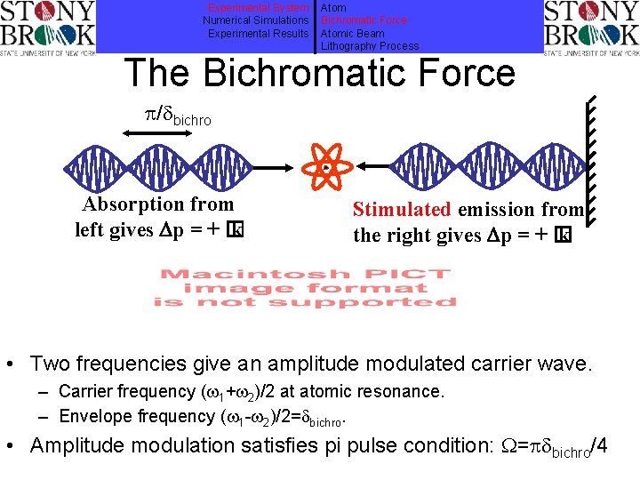
Experimental System Numerical Simulations Experimental Results Atom Bichromatic Force Atomic Beam Lithography Process The Bichromatic Force / bichro Absorption from left gives p = + � k Stimulated emission from the right gives p = + � k • Two frequencies give an amplitude modulated carrier wave. – Carrier frequency ( 1+ 2)/2 at atomic resonance. – Envelope frequency ( 1 - 2)/2= bichro. • Amplitude modulation satisfies pi pulse condition: = bichro/4
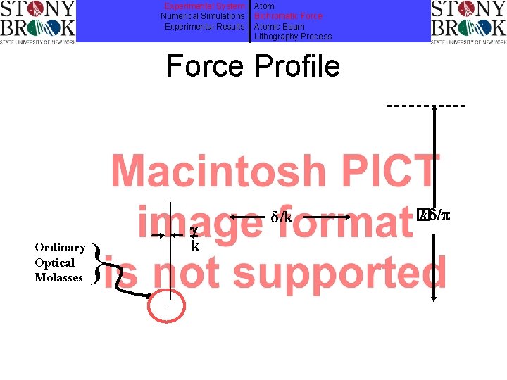
Experimental System Numerical Simulations Experimental Results Atom Bichromatic Force Atomic Beam Lithography Process Force Profile { Ordinary Optical Molasses k δ/k � k /
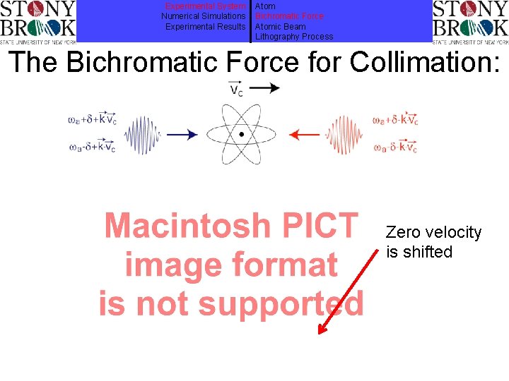
Experimental System Numerical Simulations Experimental Results Atom Bichromatic Force Atomic Beam Lithography Process The Bichromatic Force for Collimation: Zero velocity is shifted
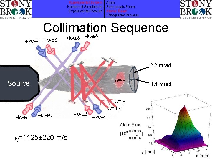
Experimental System Numerical Simulations Experimental Results +kv± Atom Bichromatic Force Atomic Beam Lithography Process Collimation Sequence -kv± +kv± 2. 3 mrad =- Source -kv± +kv± vl=1125± 220 m/s -kv± =-5 +kv± 1. 1 mrad
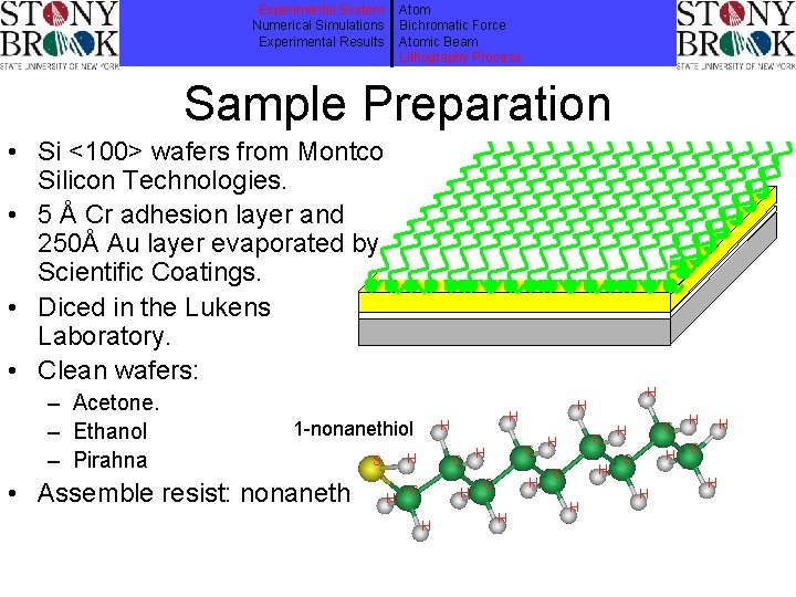
Experimental System Numerical Simulations Experimental Results Atom Bichromatic Force Atomic Beam Lithography Process Sample Preparation • Si <100> wafers from Montco Silicon Technologies. • 5 Å Cr adhesion layer and 250Å Au layer evaporated by Scientific Coatings. • Diced in the Lukens Laboratory. • Clean wafers: – Acetone. – Ethanol – Pirahna 1 -nonanethiol • Assemble resist: nonanethiol.
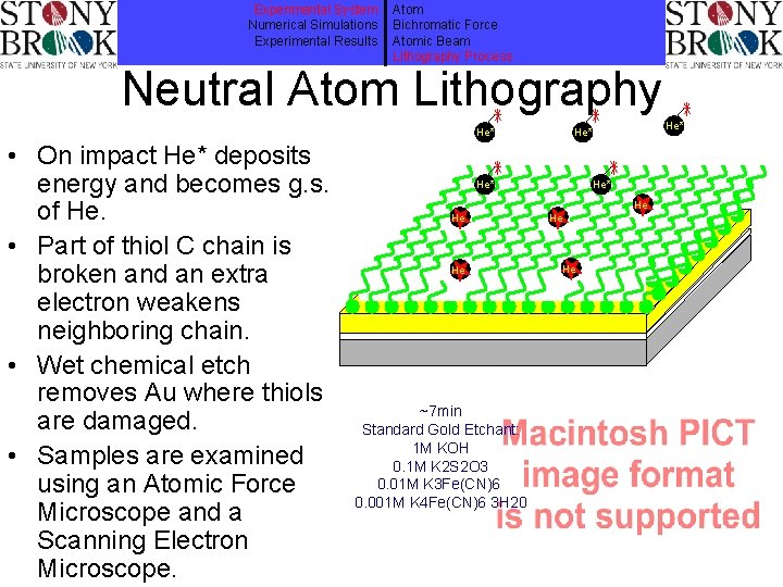
Experimental System Numerical Simulations Experimental Results Atom Bichromatic Force Atomic Beam Lithography Process Neutral Atom Lithography He* • On impact He* deposits energy and becomes g. s. of He. • Part of thiol C chain is broken and an extra electron weakens neighboring chain. • Wet chemical etch removes Au where thiols are damaged. • Samples are examined using an Atomic Force Microscope and a Scanning Electron Microscope. He* He* He He He ~7 min Standard Gold Etchant: 1 M KOH 0. 1 M K 2 S 2 O 3 0. 01 M K 3 Fe(CN)6 0. 001 M K 4 Fe(CN)6 3 H 20 He He
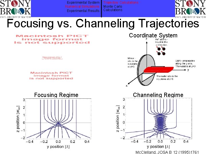
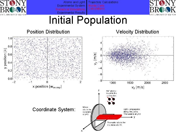
Experimental System Numerical Simulations Experimental Results Trajectory Calculations Monte Carlo Calculations Focusing vs. Channeling Trajectories Coordinate System Focusing Regime Channeling Regime Mc. Clelland, JOSA B 12 (1995)1761
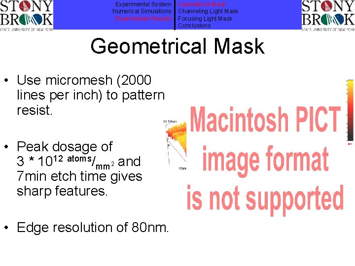
Experimental System Numerical Simulations Experimental Results Geometrical Mask Channeling Light Mask Focusing Light Mask Conclusions Geometrical Mask • Use micromesh (2000 lines per inch) to pattern resist. • Peak dosage of 3 * 1012 atoms/mm 2 and 7 min etch time gives sharp features. • Edge resolution of 80 nm.
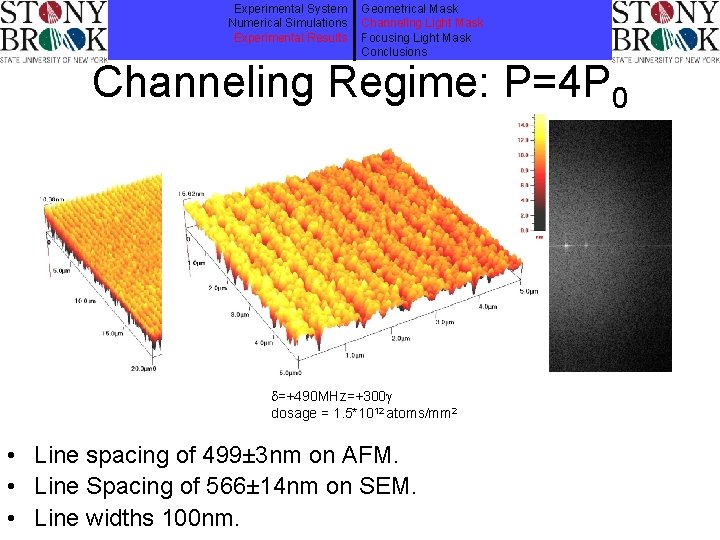
Experimental System Numerical Simulations Experimental Results Geometrical Mask Channeling Light Mask Focusing Light Mask Conclusions Channeling Regime: P=4 P 0 =+490 MHz=+300 dosage = 1. 5*1012 atoms/mm 2 • Line spacing of 499± 3 nm on AFM. • Line Spacing of 566± 14 nm on SEM. • Line widths 100 nm.
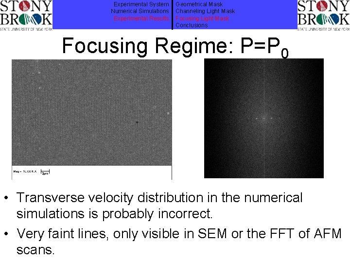
Experimental System Numerical Simulations Experimental Results Geometrical Mask Channeling Light Mask Focusing Light Mask Conclusions Focusing Regime: P=P 0 • Transverse velocity distribution in the numerical simulations is probably incorrect. • Very faint lines, only visible in SEM or the FFT of AFM scans.
Experimental System Numerical Simulations Experimental Results Channeling Light Mask Focusing Light Mask Velocity Offset Conclusions Results • Performed numerical simulations. • Measured the edge resolution to be ~80 nm. This is limited by wafer processing techniques. • Demonstrated patterning in the focusing and channeling regime.
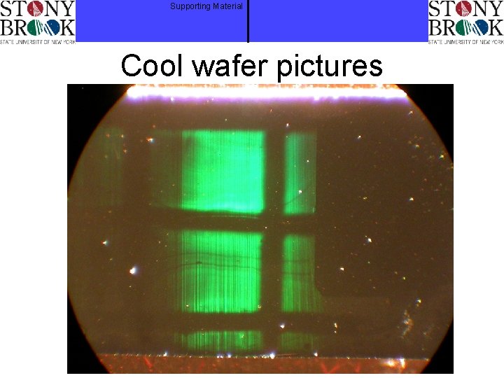
Supporting Material Cool wafer pictures
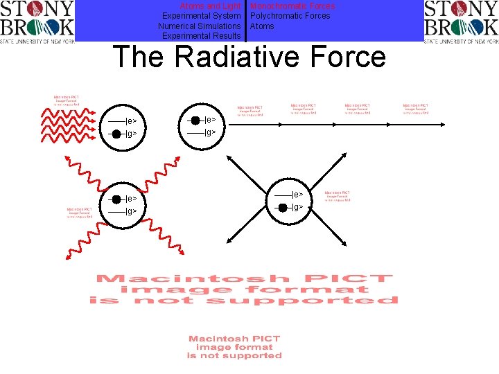
Atoms and Light Experimental System Numerical Simulations Experimental Results Monochromatic Forces Polychromatic Forces Atoms The Radiative Force |e> |g>
Atoms and Light Experimental System Numerical Simulations Experimental Results Monochromatic Forces Polychromatic Forces Atoms Force [hk /2] Optical Molasses
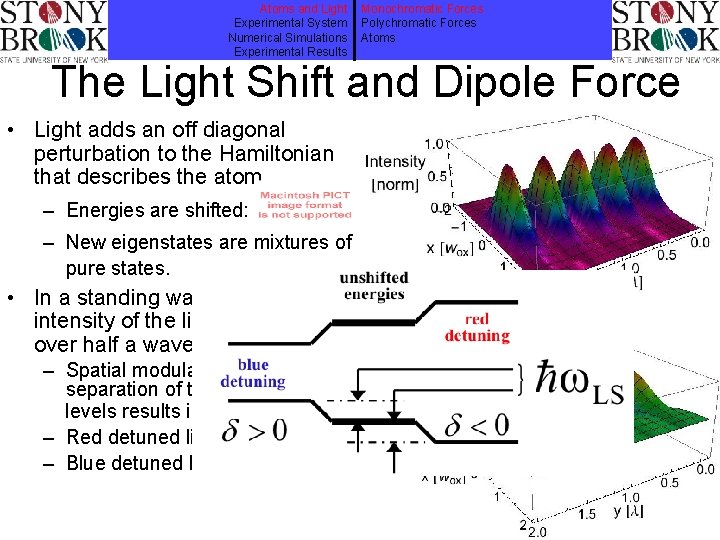
Atoms and Light Experimental System Numerical Simulations Experimental Results Monochromatic Forces Polychromatic Forces Atoms The Light Shift and Dipole Force • Light adds an off diagonal perturbation to the Hamiltonian that describes the atom. – Energies are shifted: – New eigenstates are mixtures of pure states. • In a standing wave light field, the intensity of the light changes over half a wavelength. – Spatial modulation of the separation of the energy levels results in a force. – Red detuned light attracts atoms. – Blue detuned light repels atoms.
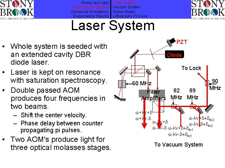
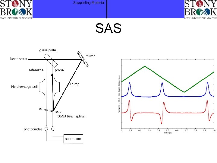
Atoms and Light Experimental System Numerical Simulations Experimental Results Laser System Vacuum System Atomic Beam Lithography Process Laser System • Whole system is seeded with an extended cavity DBR diode laser. • Laser is kept on resonance with saturation spectroscopy. • Double passed AOM produces four frequencies in two beams. – Shift the center velocity. – Phase delay between counter propagating pi pulses. • Two AOM's produce light for three optical molasses stages. PZT Diode To Lock 60 MHz 82 89 Fiber Amplifiers MHz +kv+ +kv- 90 MHz -kv+ m 2 -kv+ -kv- m 2 -kv- -kv+ m 1 -kv- m 1 To Vacuum System
Supporting Material SAS
Atoms and Light Experimental System Numerical Simulations Experimental Results Laser System Vacuum System Atomic Beam Lithography Process Vacuum System
Supporting Material OBE's
Atoms and Light Experimental System Numerical Simulations Experimental Results Trajectory Calculations Monte Carlo Calculations Initial Population Position Distribution Coordinate System: Velocity Distribution
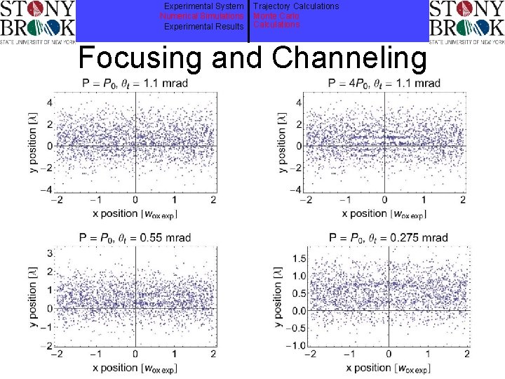
Experimental System Numerical Simulations Experimental Results Trajectory Calculations Monte Carlo Calculations Focusing and Channeling
Supporting Material Standard Selective Etch ~7 min Standard Gold Etchant: 1 M KOH 0. 1 M K 2 S 2 O 3 0. 01 M K 3 Fe(CN)6 0. 001 M K 4 Fe(CN)6 3 H 20 Metal Oxidation Or Reduction of Oxidizer
- Slides: 27