n In Ga N LDLEDVCSEL 200 nm 570
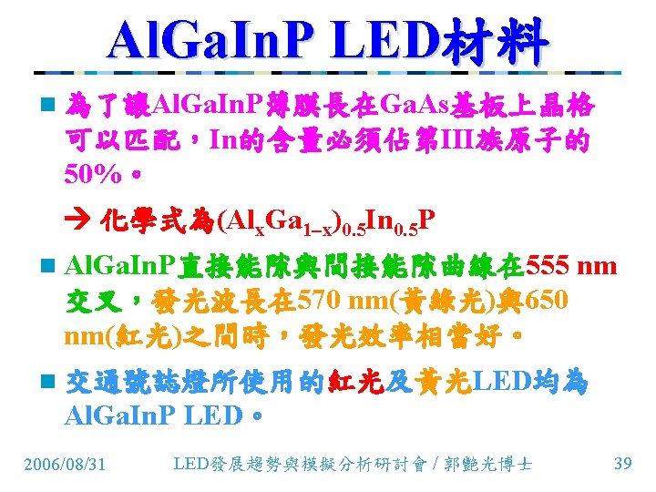
 n Al.")


0. 5 In 0. 5 P In.")
, and hence the development")


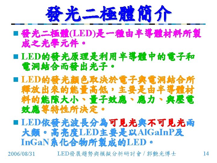
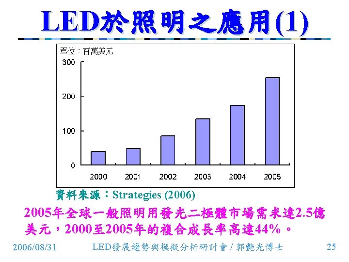
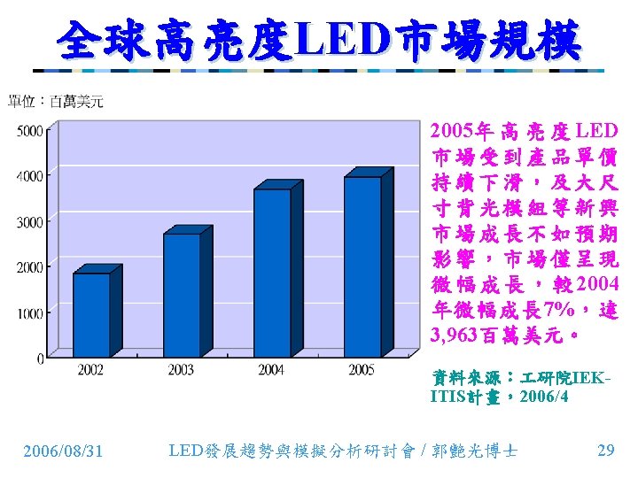
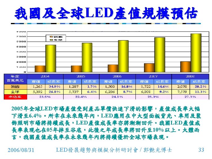
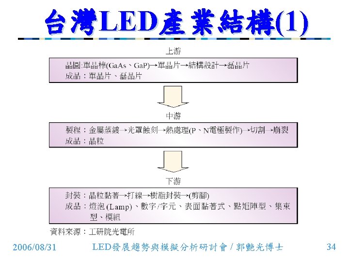
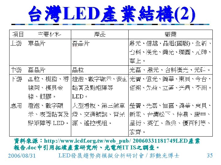
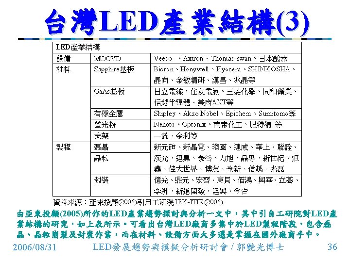
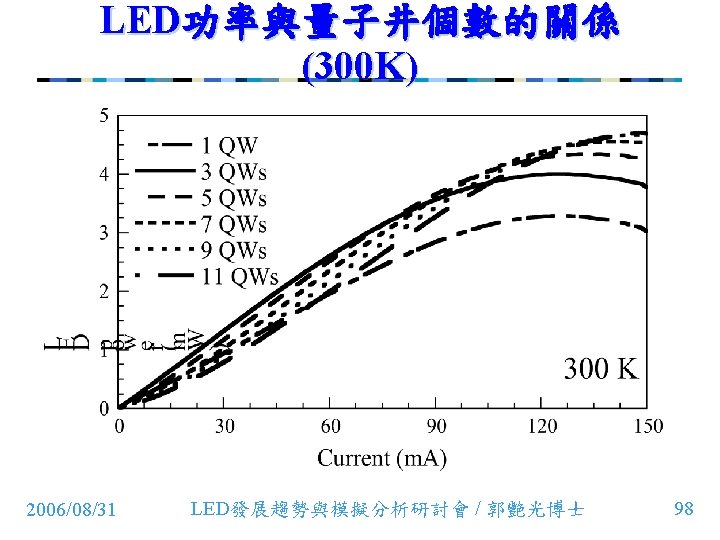
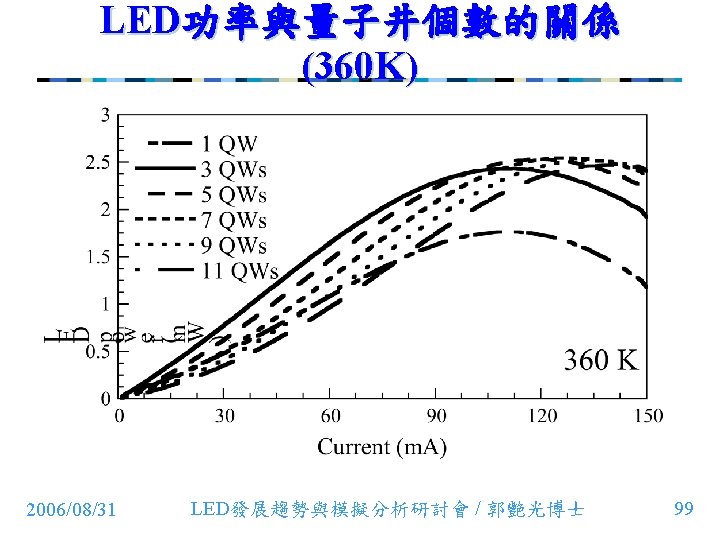
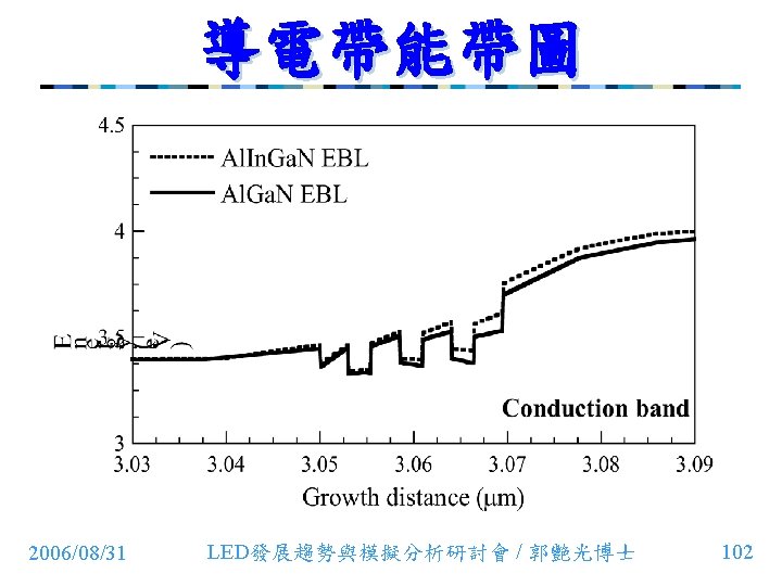
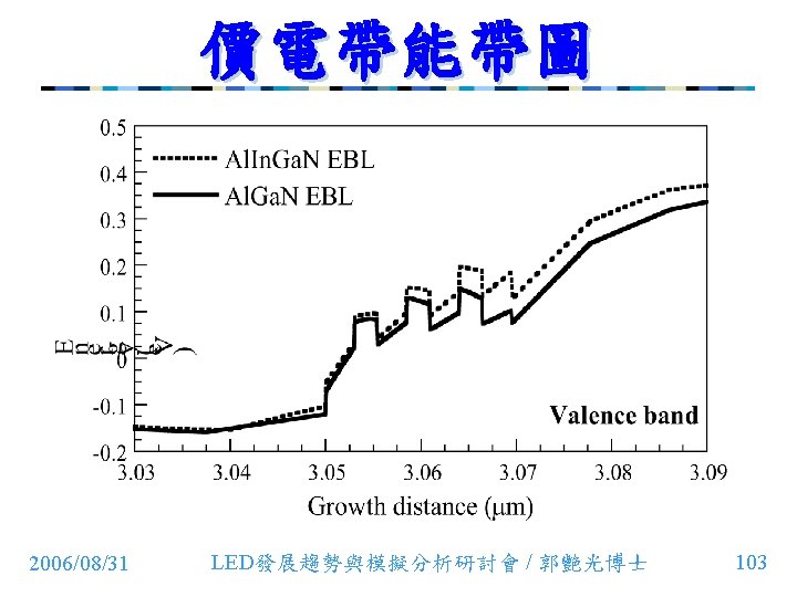
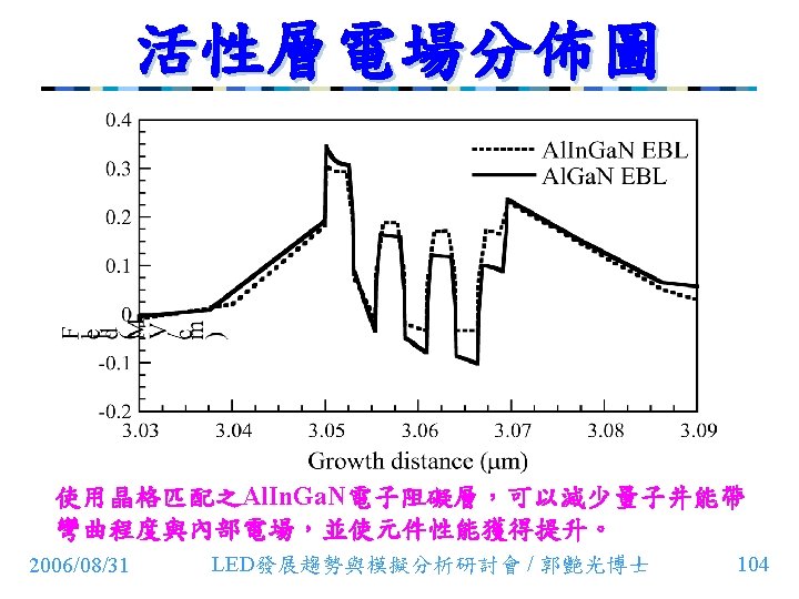
 2006/08/31 LED發展趨勢與模擬分析研討會")


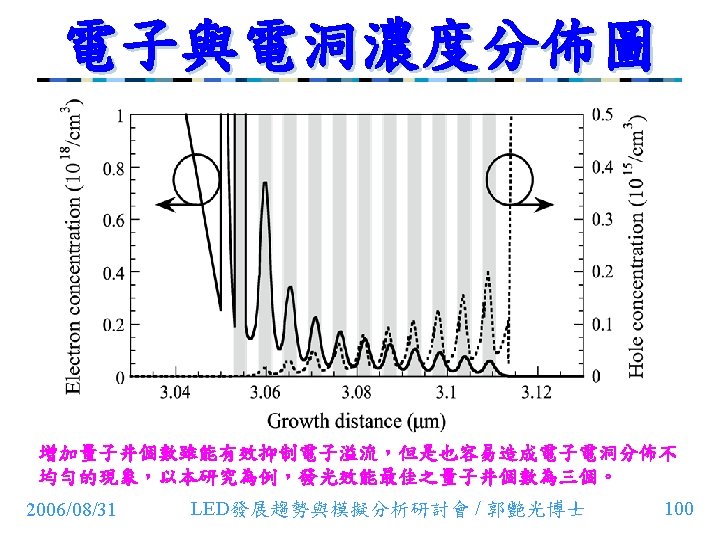
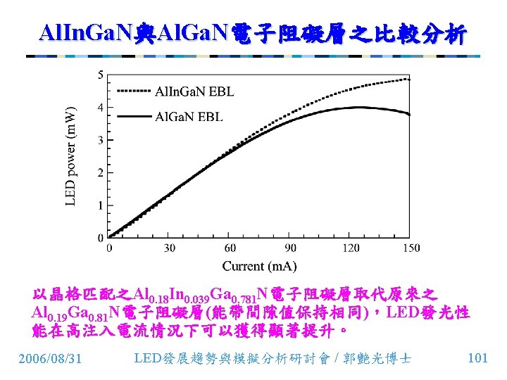
 100 Al. Ga.")
作電極 ITO window p-Cladding Active Region n-Cladding Ga. As Substrate 2006/08/31")

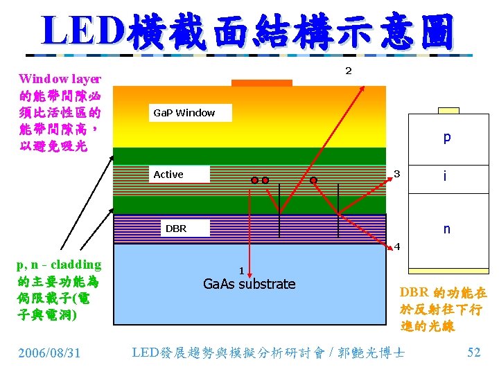
在LED的應用 p- metal Window layer x n (Eg ) Cladding layer Active layer N-pairs")

 Window, Ga. P p-Cladding Active n-Cladding Ga. P Substrate Ga. As Substrate 2006/08/31")


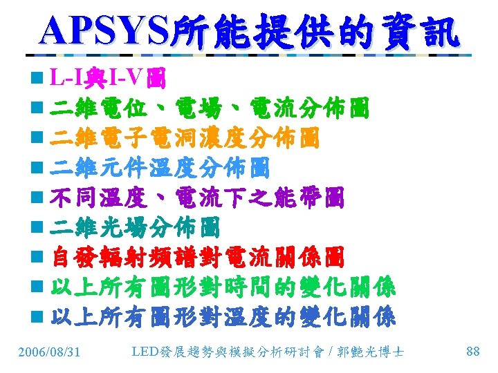
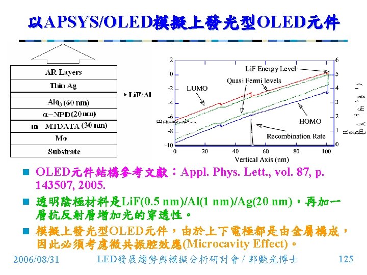
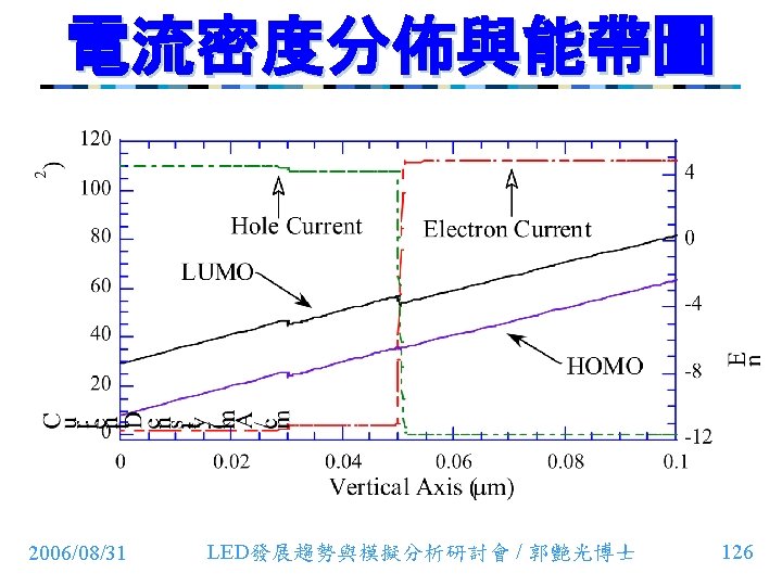
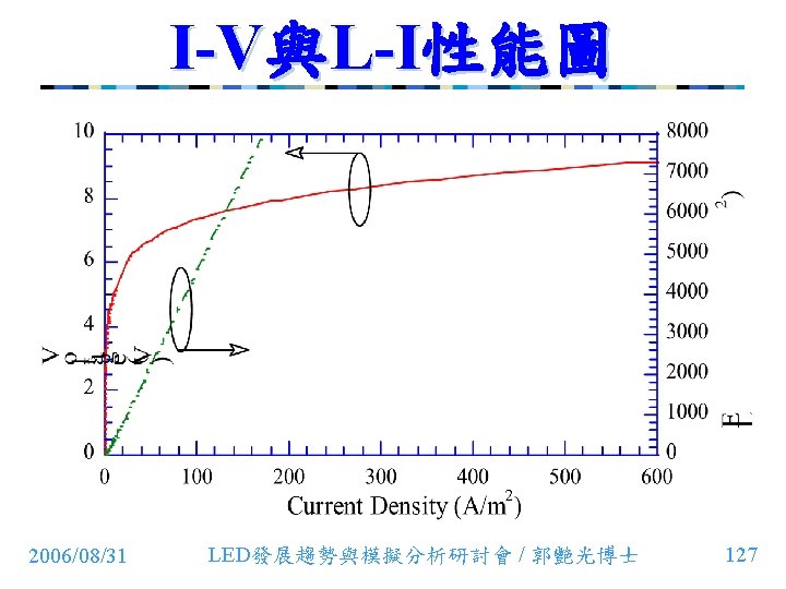
 n 此次演講所使用的LED與OLED元件模擬範 例,均借助於APSYS模擬軟體。 n APSYS可以經由解Poisson’s equation、 current")


- Slides: 133
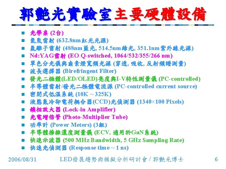
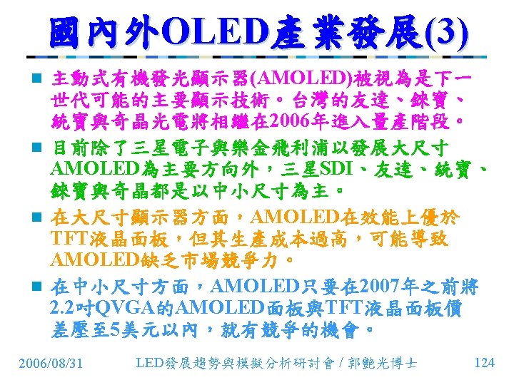
郭艷光實驗室最近研究主題 n In. Ga. N LD/LED/VCSEL (200 nm < < 570 nm) n Al. Ga. In. P LD/LED/VCSEL (570 nm < < 680 nm) n Al. Ga. In. As/In. Ga. As. P/Al. Ga. As LD/LED/VCSEL ( = 1. 3 mm, 1. 55 mm, 850 nm) n In. Ga. As. N/In. Ga. As. NSb LD/VCSEL ( = 1. 3 mm, 1. 55 mm) n 有機發光二極體(Organic 2006/08/31 OLED, OLED) LED發展趨勢與模擬分析研討會 / 郭艷光博士 4
設計與分析 具的使用 n 紫外線LED:APSYS模擬軟體 n 392 -461 nm藍紫光雷射二極體:LASTIP模 擬軟體 n 850 -nm VCSEL:PICS 3 D模擬軟體 n 上發光型OLED元件:APSYS/OLED模擬 軟體 n 模擬軟體購自Crosslight Software Inc. http: //www. crosslight. com/ n Free training license: http: //www. crosslight. com/downloads. html#Tra ining_license 2006/08/31 LED發展趨勢與模擬分析研討會 / 郭艷光博士 9
參考文獻 n n n Yi-An Chang, Sheng-Horng Yen, De-Chung Wang, Hao-Chung Kuo, Yen. Kuang Kuo, and Shing-Chung Wang, 21 March 2006, “Experimental and theoretical analysis on ultraviolet 370 -nm Al. Ga. In. N light-emitting diode”, Semiconductor Science and Technology, Vol. 21, pp. 598 -603. Jun-Rong Chen and Yen-Kuang Kuo, 1 August 2006, “Optical gain and threshold properties of strained In. Ga. Al. As/Al. Ga. As quantum wells for 850 -nm vertical-cavity surface-emitting lasers”, Optics Communications, Vol. 264, pp. 213 -218. Yi-An Chang, Jun-Rong Chen, Hao-Chung Kuo, Yen-Kuang Kuo, and Shing. Chung Wang, January 2006, “Theoretical and experimental analysis on In. Al. Ga. As/Al. Ga. As active region of 850 -nm vertical-cavity surface-emitting lasers”, Journal of Lightwave Technology, Vol. 24, No. 1, pp. 536 -543. Yen-Kuang Kuo and Yi-An Chang, May 2004, “Effects of electronic current overflow and inhomogeneous carrier distribution on In. Ga. N quantum-well laser performance”, IEEE Journal of Quantum Electronics, Vol. 40, No. 5, pp. 437 -444. Yen-Kuang Kuo, Bo-Ting Liou, Mei-Ling Chen, Sheng-Horng Yen, and Cheng -Yang Lin, 15 February 2004, “Effect of band-offset ratio on analysis of violetblue In. Ga. N laser characteristics”, Optics Communications, Vol. 231, Issues 16, pp. 395 -402. 張詒安、郭艷光、郭浩中、王興宗, 2004年3月, “紫藍光氮化銦鎵量子井雷射 之模擬與分析”, 光學 程, 第 85期, 第 47至 58頁. 2006/08/31 LED發展趨勢與模擬分析研討會 / 郭艷光博士 11
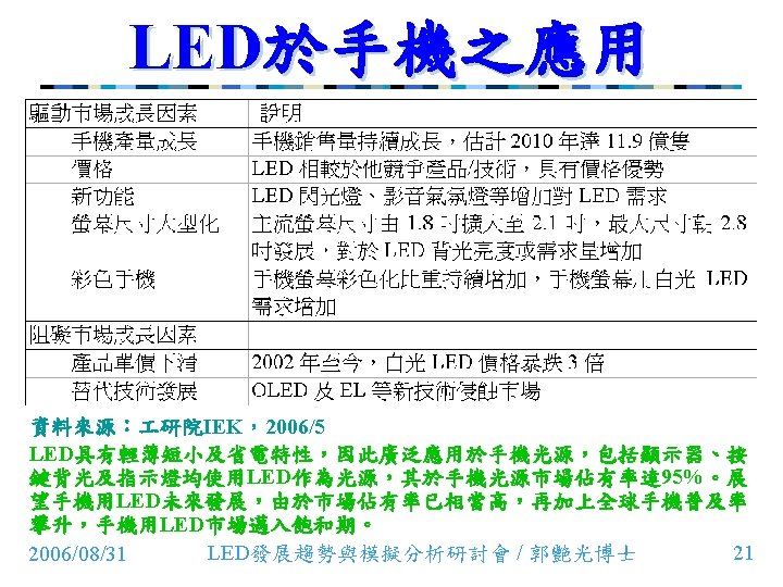
LED分類與應用 In. Ga. As、Al. Ga. As In. Ga. As. P、Al. Ga. In. As 資料來源:http: //www. icdf. org. tw/web_pub/ 20060331181749 LED產業報告. doc LED發展趨勢與模擬分析研討會 / 郭艷光博士 15 2006/08/31
LED用於LCD TV背光源優劣勢比較 http: //tech. digitimes. com. tw/Show. News. aspx? z. Cat. Id=116&z. Notes. Doc. Id=C E 07 A 4130262 B 4 DE 4825718 C 00344 ADF 2006/08/31 LED發展趨勢與模擬分析研討會 / 郭艷光博士 17
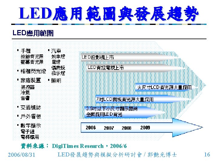
LED用於LCD TV背光源技術改善方式及達成目標 資料來源:Digi. Times Research,2006/6 http: //tech. digitimes. com. tw/Show. News. aspx? z. Cat. Id=116&z. Notes. Doc. Id =CE 07 A 4130262 B 4 DE 4825718 C 00344 ADF(2006/06/14 2006/08/31 LED發展趨勢與模擬分析研討會 / 郭艷光博士 18
2006~2009年40吋LED背光模組價格預估 資料來源:Digi. Times Research,2006/6 http: //tech. digitimes. com. tw/Show. News. aspx? z. Cat. Id=116&z. Notes. Doc. Id=CE 0 7 A 4130262 B 4 DE 4825718 C 00344 ADF 2006/08/31 LED發展趨勢與模擬分析研討會 / 郭艷光博士 19
LED應用於Citizen 40吋LCD TV背光模組 資料來源:Citizen,2006/4 http: //tech. digitimes. com. tw/Show. News. aspx? z. Cat. Id=C 14&z. Notes. Doc. Id=5 6060 C 2 DD 3 E 7 E 4 E 7482571 B 800616 E 6 A 2006/08/31 LED發展趨勢與模擬分析研討會 / 郭艷光博士 20
光電半導體材料 I II IIb 3 Li 4 Be 11 Na 12 Mg 19 K 20 Ca 30 37 Rb 38 Sr 48 55 Cs 56 Ba Zn Cd 80 Hg III IV 5 B 6 C VI N 8 O 7 Al 14 Ga 32 Ge 33 As 34 49 In 50 Sn 51 Sb 52 81 Tl 82 Pb 83 Bi 84 Po 13 31 Si V P 15 S 16 Se Te IV: Photo-detector III-V & II-VI: LED/LD & Photo-detector 2006/08/31 LED發展趨勢與模擬分析研討會 / 郭艷光博士 37
可見光區的光電半導體材料 Al. Ga. As (Alx. Ga 1 -x)0. 5 In 0. 5 P In. Ga. N 300 400 500 600 700 Dominant Wavelength , D ( nm ) 2006/08/31 LED發展趨勢與模擬分析研討會 / 郭艷光博士 38
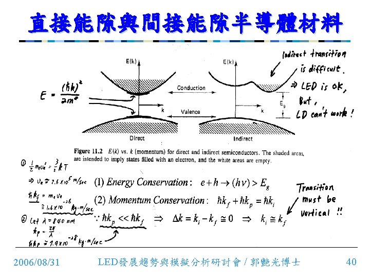
人眼對光之敏感度頻譜 Human eyes are sensitive to green light (~555 nm), and hence the development of green (or yellowish green) Al. Ga. In. P LED is desirable. 2006/08/31 LED發展趨勢與模擬分析研討會 / 郭艷光博士 41
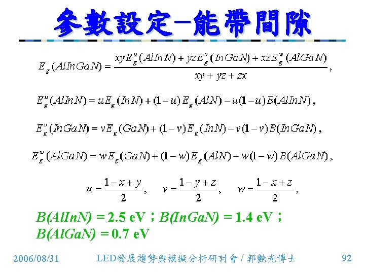
Inx. Ga 1 -x. N LED的發光範圍 Eg x · Eg, In. N + (1 -x) · Eg, Ga. N – b · x · (1 -x) b Bowing Parameter Eg, In. N = 0. 77 e. V, Eg, Ga. N = 3. 42 e. V, b = 1. 43 e. V Reference: Wu et al. , Appl. Phys. Lett. 80, 4741, 2002. III-N is very efficient between 250 nm and 570 nm. 2006/08/31 LED發展趨勢與模擬分析研討會 / 郭艷光博士 43
In. Ga. N LED的結構 p-Electrode p-Ga. N 正負電極都在 基板的上方!! p-Alx. Ga 1 -x. N Iny. Ga 1 -y. N n-Alz. Ga 1 -z. N n-Electrode n-Ga. N Buffer Layer Sapphire Substrate 2006/08/31 LED發展趨勢與模擬分析研討會 / 郭艷光博士 44
Nichia公司在 1997年發表的In. Ga. N半導體雷射 ELOG Substrate (Epitaxially Laterally Overgrown Ga. N Substrate) 2006/08/31 LED發展趨勢與模擬分析研討會 / 郭艷光博士 45
雙異質結構的電子與光子侷限 Undoped Active Layer n-type Layer p-type Layer ~0. 2μm Electrons Energy Conduction Band Gap Carrier Confinement Valence Band Holes Index n 1 n 2 Mode Profile Light 2006/08/31 Optical Confinement LED發展趨勢與模擬分析研討會 / 郭艷光博士 46
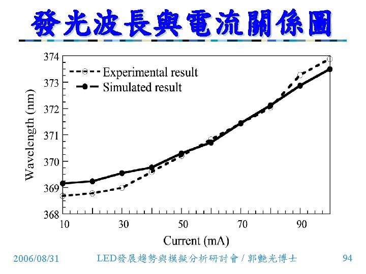
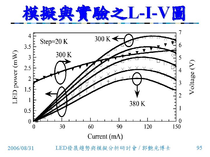
LED發光基本特性 Wavelength Vs. Current 610 250 12 mil 9 mil 8 mil 200 Wavelength (nm) Lumen Intensity (mcd) Intensity Vs. Current 150 100 50 0 0 12 mil 605 9 mil 8 mil 600 595 590 585 20 40 60 80 100 Current (m. A) LED發光強度有極大值 (亦即有飽和的現象) 2006/08/31 120 580 0 20 40 60 80 100 120 Current (m. A) LED發光波長會隨注入 電流(及溫度)增加而增加 LED發展趨勢與模擬分析研討會 / 郭艷光博士 53
Al. Ga. In. P與In. Ga. N發光二極體 Luminous Efficiency ( lumen/Watt ) 100 Al. Ga. In. P In. Ga. N Ga. P Sapphire 10 Al. Ga. In. P Ga. As Al. Ga. As Ga. P: N 1 Ga. As. P: N Ga. P 0. 1 420 500 580 660 Wavelength ( nm ) 2006/08/31 LED發展趨勢與模擬分析研討會 / 郭艷光博士 54
使用ITO (Indium Tin Oxide)作電極 ITO window p-Cladding Active Region n-Cladding Ga. As Substrate 2006/08/31 LED發展趨勢與模擬分析研討會 / 郭艷光博士 56
使用Current-Blocking設計 Regrowth p-window n-blocking p-Cladding Buried n-blocking p-Cladding Active n-Cladding Ga. As Substrate 1 st Growth 2006/08/31 Etching Ga. As Substrate 2 nd Growth LED發展趨勢與模擬分析研討會 / 郭艷光博士 57
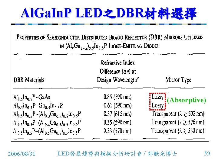
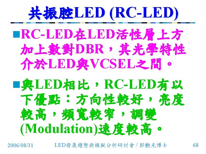
布拉格反射鏡(DBR)在LED的應用 p- metal Window layer x n (Eg ) Cladding layer Active layer N-pairs DBR Alx. Ga 1 -x. As Substrate Aly. Ga 1 -y. As /4 n 1 /4 n 2 n- metal DBR設計準則:兩層都不能吸光,折射率差越大越好。 2006/08/31 LED發展趨勢與模擬分析研討會 / 郭艷光博士 58
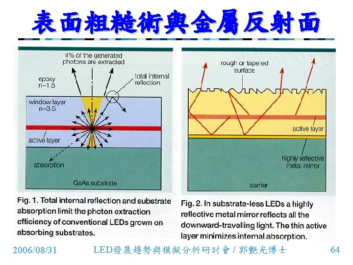
透明與不透明DBR的差異 Transparent DBR Lossy DBR 2006/08/31 Reflectivity can never approach to 1. 0. LED發展趨勢與模擬分析研討會 / 郭艷光博士 60
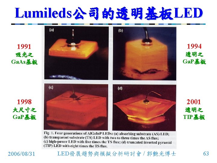
使用透明基板(向下發光) Window, Ga. P p-Cladding Active n-Cladding Ga. P Substrate Ga. As Substrate 2006/08/31 LED發展趨勢與模擬分析研討會 / 郭艷光博士 61
光子與電子之間的交互作用 Before Process Absorption Emission EC EV EV Photodetector EC Emission Example EC l Spontaneous Stimulated After EV Eg EC l 1 EV EC EV Light Emitting Diode OLED EC l 1 Laser Diode l 2 RC-LED ? EV ( in phase ) ( nm ) = 1240 / Eg ( e. V ) 2006/08/31 LED發展趨勢與模擬分析研討會 / 郭艷光博士 67
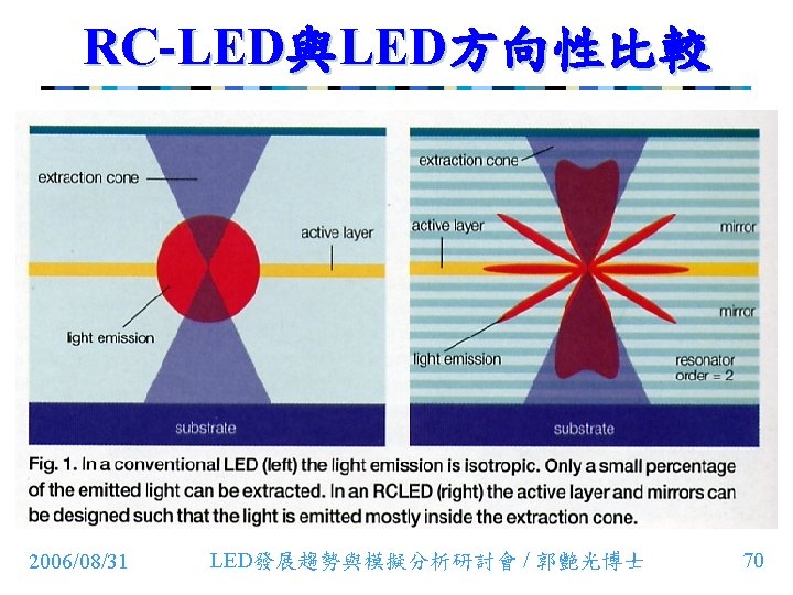
RC-LED結構示意圖 Contact layer 上DBR: R ~ 0. 6 -0. 7 共振腔 下DBR: R ~ 1. 0 Absorbing substrate 2006/08/31 LED發展趨勢與模擬分析研討會 / 郭艷光博士 69
630 -nm n-type Modulation-Doped Al. Ga. In. P-Al. In. P MQW LED IEEE Photon. Technol. Lett. vol. 18, p. 25, 2006/08/31 LED發展趨勢與模擬分析研討會 / 郭艷光博士 73
Titanium Nitride as Spreading Layers for Al. Ga. In. P Visible LEDs IEEE Photon. Technol. Lett. vol. 14, p. 1665, 2002. 2006/08/31 LED發展趨勢與模擬分析研討會 / 郭艷光博士 74
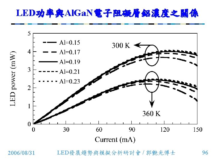
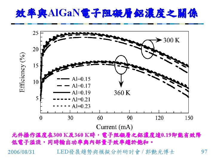
Titanium Nitride as Spreading Layers for Al. Ga. In. P Visible LEDs n Al. Ga. In. P LED在使用Ti. N Spreading Layer之後, 在高注入電流時所產生之電流聚集以及輸出功率 飽和的情況已經獲得改善。 2006/08/31 LED發展趨勢與模擬分析研討會 / 郭艷光博士 75
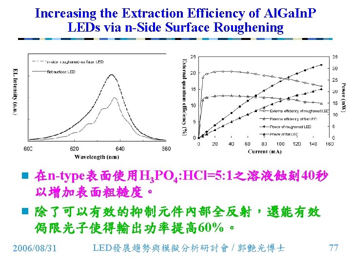
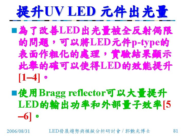
Increasing the Extraction Efficiency of Al. Ga. In. P LEDs via n-Side Surface Roughening IEEE Photon. Technol. Lett. vol. 17, p. 2289, 2005. 2006/08/31 LED發展趨勢與模擬分析研討會 / 郭艷光博士 76
Fabrication of p-Side Down Ga. N Vertical Light-Emitting Diodes on Copper Substrates by Laser Lift-Off Phys. Stat. Sol. (C) vol. 1, p. 2413, 2004. 2006/08/31 LED發展趨勢與模擬分析研討會 / 郭艷光博士 79
參考文獻 1. 2. 3. 4. 5. 6. 7. 8. 9. IEEE Photon. Technol. Lett. , vol. 17, p. 983, 2005. IEEE Photon. Technol. Lett. , vol. 17, p. 2038, 2005. Appl. Phys. Lett. , vol. 88, p. 181117, 2006. Appl. Phys. Lett. , vol. 89, p. 041116, 2006. Phys. Stat. Sol. (a), vol. 202, p. 2836, 2005. Phys. Stat. Sol. (a), vol. 201, p. 2653, 2004. Phys. Stat. Sol. (a), vol. 201, p. 2786, 2004. Phys. Stat. Sol. (c), vol. 3, p. 2199, 2006. Phys. Stat. Sol. (a), vol. 200, p. 110, 2003. 2006/08/31 LED發展趨勢與模擬分析研討會 / 郭艷光博士 84
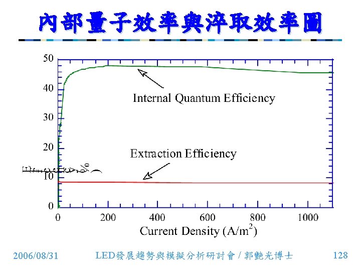
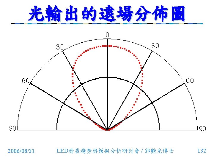
APSYS模擬軟體 (Advanced Physical Models of Semiconductor Devices) n 此次演講所使用的LED與OLED元件模擬範 例,均借助於APSYS模擬軟體。 n APSYS可以經由解Poisson’s equation、 current continuity equation、carrier energy transport equation、以及quantum mechanical wave equation等方程式,求得 光電半導體元件的各種光學與電子特性。 n APSYS亦使用Ray-Tracing技術,分析由元 件所輸出之光強度以及光場隨角度之分佈 情形。 2006/08/31 LED發展趨勢與模擬分析研討會 / 郭艷光博士 87
紫外光發光二極體模擬−參考文獻 Yi-An Chang, Sheng-Horng Yen, De-Chung Wang, Hao-Chung Kuo, Yen-Kuang Kuo, and Shing-Chung Wang, 21 March 2006, “Experimental and theoretical analysis on ultraviolet 370 -nm Al. Ga. In. N light-emitting diode”, Semiconductor Science and Technology, Vol. 21, pp. 598 -603. (SCI) (EI) n Yen-Kuang Kuo, Sheng-Horng Yen, and Jun. Rong Chen, 2006, Ultraviolet Light-Emitting Diodes, in Nitride Semiconductor Devices: Principles and Simulation (Chapter 15), edited by Joachim Piprek, to be published by Wiley-VCH, the German branch of Wiley & Sons. n 2006/08/31 LED發展趨勢與模擬分析研討會 / 郭艷光博士 89
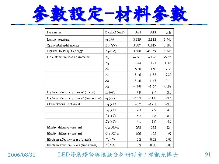
UV LED結構圖 Semicond. Sci. Technol. , vol. 21, p. 598, 2006/08/31 LED發展趨勢與模擬分析研討會 / 郭艷光博士 90
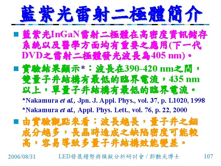
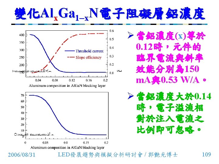
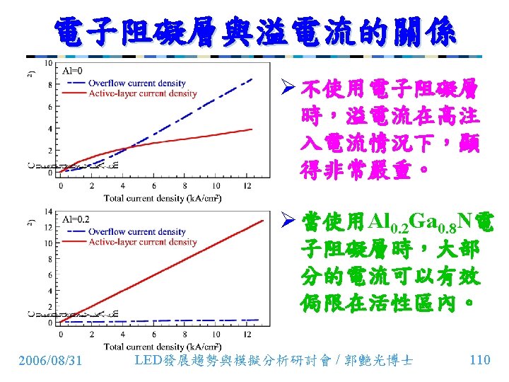
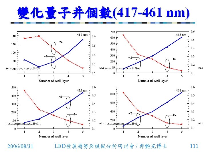
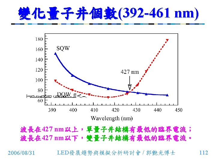
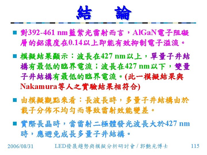
藍紫光雷射二極體模擬分析 n 此一研究成果已發表於IEEE Journal of Quantum Electronics。 n Yen-Kuang Kuo and Yi-An Chang, May 2004, “Effects of electronic current overflow and inhomogeneous carrier distribution on In. Ga. N quantum-well laser performance”, IEEE Journal of Quantum Electronics, Vol. 40, No. 5, pp. 437 -444. (SCI) (EI) n 本文探討392 -461 nm雷射二極體的光學與電 子特性,以及最佳化分析。 2006/08/31 LED發展趨勢與模擬分析研討會 / 郭艷光博士 106
模擬之雷射二極體結構 p-contact 0. 1 -mm p-Ga. N 1. 0 -mm p-Al 0. 07 Ga 0. 93 N 0. 1 -mm p-Ga. N 0. 02 -mm p-Al 0. 2 Ga 0. 8 N undoped active region n-contact 0. 1 -mm n-Ga. N 1. 0 -mm n-Al 0. 07 Ga 0. 93 N 0. 1 -mm n-In 0. 1 Ga 0. 9 N 3. 0 -mm n-Ga. N 2006/08/31 LED發展趨勢與模擬分析研討會 / 郭艷光博士 108
Thank you for your attention! LED發展趨勢與模擬分析研討會 / 郭艷光博士 彰化師大郭艷光 http: //ykuo. ncue. edu. tw 133 2006/08/31