n CHAPTER 4 n Combinational Logic Designn Arithmetic
n CHAPTER 4 n Combinational Logic Designn Arithmetic Operation n (Section 4. 6&4. 9)

Overview n Binary Addition Ø Half Adder Ø Full Adder Ø Ripple Carry Adder(并行加法器) Ø Carry Look ahead Adder(超前进位加法器) Decimal Addition (Section 4. 6. 6) n Binary Comparators (Section 4. 7 n
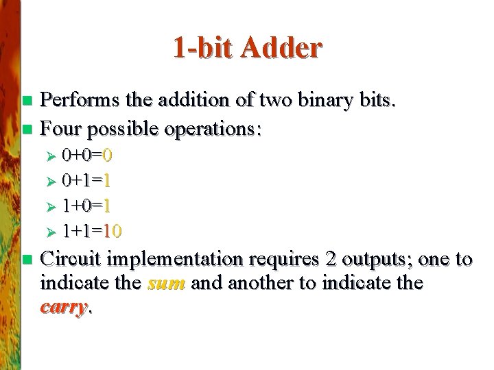
1 -bit Adder Performs the addition of two binary bits. n Four possible operations: n Ø 0+0=0 Ø 0+1=1 Ø 1+0=1 Ø 1+1=10 n Circuit implementation requires 2 outputs; one to indicate the sum and another to indicate the carry.
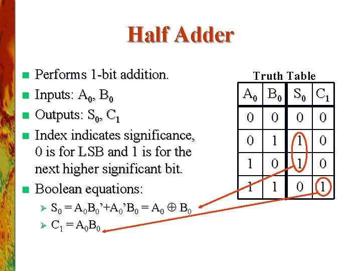
Half Adder n n n Performs 1 -bit addition. Inputs: A 0, B 0 Outputs: S 0, C 1 Index indicates significance, 0 is for LSB and 1 is for the next higher significant bit. Boolean equations: Ø Ø S 0 = A 0 B 0’+A 0’B 0 = A 0 B 0 C 1 = A 0 B 0 Truth Table A 0 B 0 S 0 C 1 0 0 0 1 1 0 1 0 1
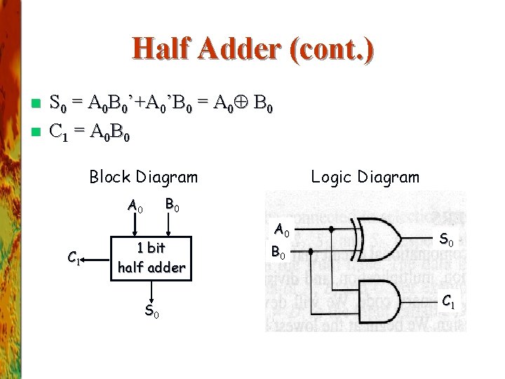
Half Adder (cont. ) n n S 0 = A 0 B 0’+A 0’B 0 = A 0 B 0 C 1 = A 0 B 0 Block Diagram B 0 A 0 C 1 Logic Diagram 1 bit half adder S 0 A 0 B 0 S 0 C 1
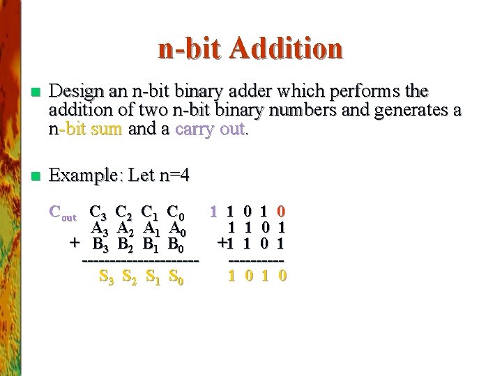
n-bit Addition n Design an n-bit binary adder which performs the addition of two n-bit binary numbers and generates a n-bit sum and a carry out. n Example: Let n=4 Cout C 3 C 2 C 1 C 0 1 1 0 A 3 A 2 A 1 A 0 1 1 0 1 + B 3 B 2 B 1 B 0 +1 1 0 1 ---------------S 3 S 2 S 1 S 0 1 0
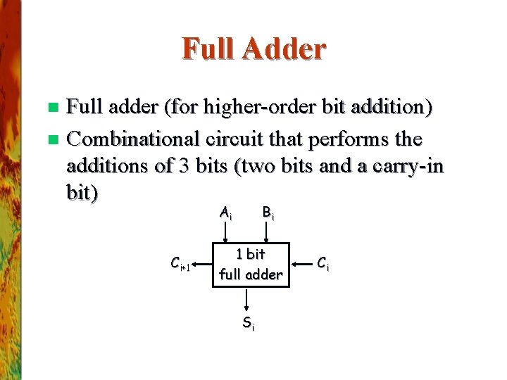
Full Adder Full adder (for higher-order bit addition) n Combinational circuit that performs the additions of 3 bits (two bits and a carry-in bit) n Ai Ci+1 Bi 1 bit full adder Si Ci
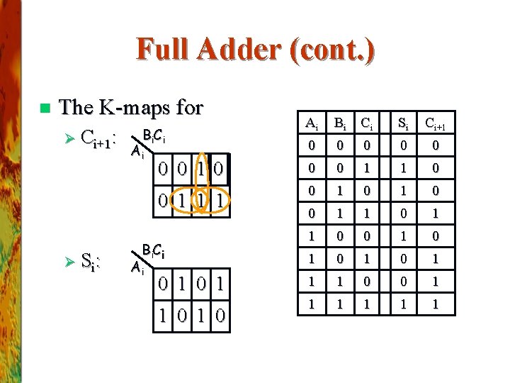
Full Adder (cont. ) n The K-maps for Ø Ci+1: Ø Si : Ai Bi Ci Si Ci+1 0 0 0 0 10 0 0 1 1 1 0 1 0 0 1 0 1 1 1 0 0 1 1 1 Bi C i Ai 0 1 1 0
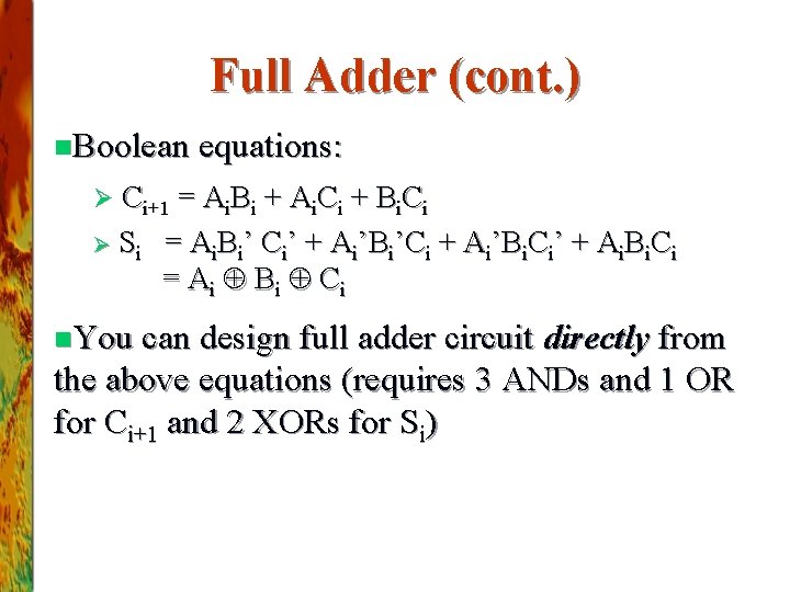
Full Adder (cont. ) n. Boolean equations: Ci+1 = Ai. Bi + Ai. Ci + Bi. Ci Ø Si = Ai. Bi’ Ci’ + Ai’Bi’Ci + Ai’Bi. Ci’ + Ai. Bi. Ci = Ai Bi Ci Ø n. You can design full adder circuit directly from the above equations (requires 3 ANDs and 1 OR for Ci+1 and 2 XORs for Si)
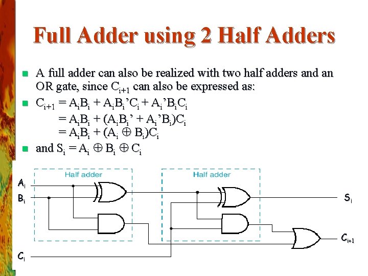
Full Adder using 2 Half Adders n n n A full adder can also be realized with two half adders and an OR gate, since Ci+1 can also be expressed as: Ci+1 = Ai. Bi + Ai. Bi’Ci + Ai’Bi. Ci = Ai. Bi + (Ai. Bi’ + Ai’Bi)Ci = Ai. Bi + (Ai Bi)Ci and Si = Ai Bi Ci Ai Bi Si Ci+1 Ci

n-bit Combinational Adders Perform parallel multi-bit addition n Ripple Carry Adder (并行加法器) n Ø Simple design Ø Time consuming. Why? (you’ll see in a bit!) n Carry Look ahead Adder (超前进位加法器) Ø More complex than ripple-carry adder Ø Reduces circuit delay
n-bit Ripple Carry Adder Constructed using n 1 -bit full adder blocks in parallel. n Cascade the full adders so that the carry out from one becomes the carry in to the next higher bit position. n
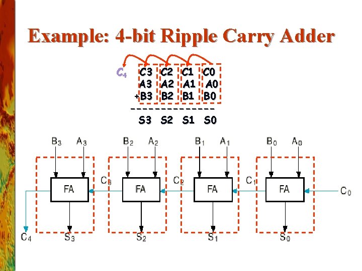
Example: 4 -bit Ripple Carry Adder C 4 C 3 C 2 C 1 C 0 A 3 A 2 A 1 A 0 +B 3 B 2 B 1 B 0 -------S 3 S 2 S 1 S 0
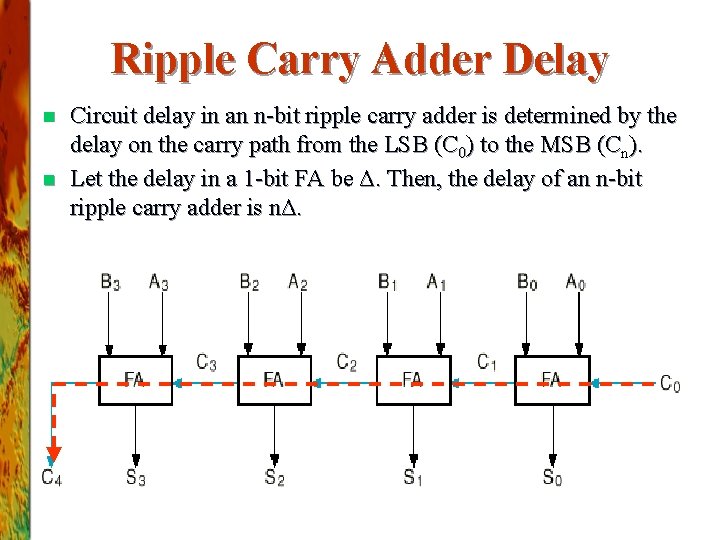
Ripple Carry Adder Delay n n Circuit delay in an n-bit ripple carry adder is determined by the delay on the carry path from the LSB (C 0) to the MSB (Cn). Let the delay in a 1 -bit FA be Δ. Then, the delay of an n-bit ripple carry adder is nΔ.

Carry Look ahead Adder Alternative design for a combinational n-bit adder. n Practical design with reduced delay at the expense of more complex hardware. n Derived from a transformation of the ripple carry adder design. n
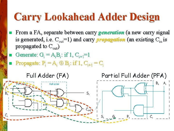
Carry Lookahead Adder Design n From a FA, separate between carry generation (a new carry signal is generated, i. e. Cout=1) and carry propagation (an existing Cin is propagated to Cout) Generate: Gi = Ai. Bi: if 1, Ci+1=1 Propagate: Pi = Ai Bi: if 1, Ci+1 = Ci Full Adder (FA) Partial Full Adder (PFA) Bi Ai Bi Si Ci+1 Ci Si Gi Pi Ci Ai
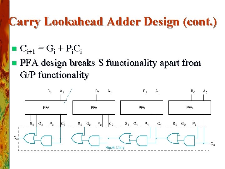
Carry Lookahead Adder Design (cont. ) Ci+1 = Gi + Pi. Ci n PFA design breaks S functionality apart from G/P functionality n
Carry Look ahead Adder (cont. ) Does this (design in previous slide) solve the long delay problem? n No, carry out still “ripples” ! n Idea: use two levels of logic to generate carry out of any block Ci in terms of carry in C 0 and addend bits Ai and Bi n

Block CLA n Implement: Ø C 1 = G 0+P 0 C 0 Ø C 2 = G 1+P 1 C 1 = G 1+P 1(G 0+P 0 C 0) = G 1+P 1 G 0+P 1 P 0 C 0 Ø C 3 = G 2 + P 2 C 2 = G 2+P 2 G 1+P 2 P 1 G 0+P 2 P 1 P 0 C 0 Ø C 4 = G 3+P 3 G 2+P 3 P 2 G 1+P 3 P 2 P 1 G 0 + P 3 P 2 P 1 P 0 C 0 = G 0 -3 + P 0 -3 C 0 Group carry generate Group carry propagate
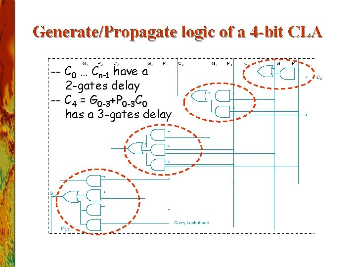
Generate/Propagate logic of a 4 -bit CLA -- C 0 … Cn-1 have a 2 -gates delay -- C 4 = G 0 -3+P 0 -3 C 0 has a 3 -gates delay
4. 6. 4 Using MSI Adders as Subtractors n MSI Adders Ø 74 LS 83 : 4 Bits carry look ahead adder device Ø Cascading four 74 LS 83 four-bit adders to form 1 16 bit adder (Fig. 4. 55) n Subtractor(P 155) Ø Using 2 s complement to realize subtraction
4. 6. 5 Using an MSI Adders as BCD to Excess-3 code converter Ø Page 156
4. 6. 6 BCD Adder n BCD Decimal Adder: Ø Requires 8 inputs (4 bits per decimal number) Ø 5 outputs indicate the decimal sum and the carry Ø Remember BCD addition rules: Add 0110 to the sum if it is greater than 1010 to correct the carry bit (P 157)
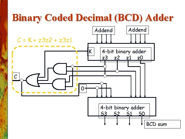
Binary Coded Decimal (BCD) Adder Addend C = K + z 3 z 2 + z 3 z 1 K 4 -bit binary adder z 3 z 2 z 1 z 0 C 0 4 -bit binary adder S 3 S 2 S 1 S 0 BCD sum
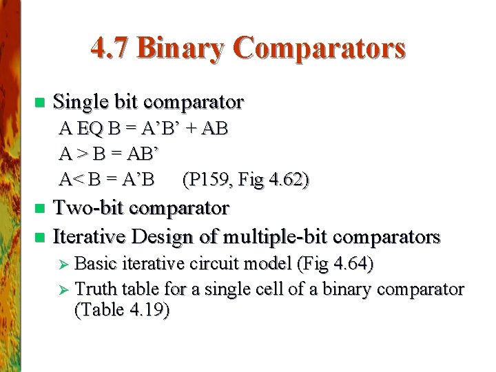
4. 7 Binary Comparators n Single bit comparator A EQ B = A’B’ + AB A > B = AB’ A< B = A’B (P 159, Fig 4. 62) Two-bit comparator n Iterative Design of multiple-bit comparators n Ø Basic iterative circuit model (Fig 4. 64) Ø Truth table for a single cell of a binary comparator (Table 4. 19)
4. 8 Arithmetic Logic Unit (ALU) Combining all possible combinational logic functions (Addition, Subtraction, AND, OR, etc. ) into a single IC. n Select bits are used to select one of the functions to be implemented (See Table 4. 21, P 164) n
Array Multipliers (Omitted) n Tri-state buffers (P 170) n 4. 11 Combinational Logic Hazards (P 171) n Ø Static ‘ 1’ hazard Ø Static ‘ 0’ hazard Ø Ex. P = xy’ + yz

- Slides: 28