Multiple Clock System Design Danny Mok Altera HK
- Slides: 35

Multiple Clock System Design Danny Mok Altera HK FAE (dmok@altera. com) Copyright © 1997 Altera Corporation

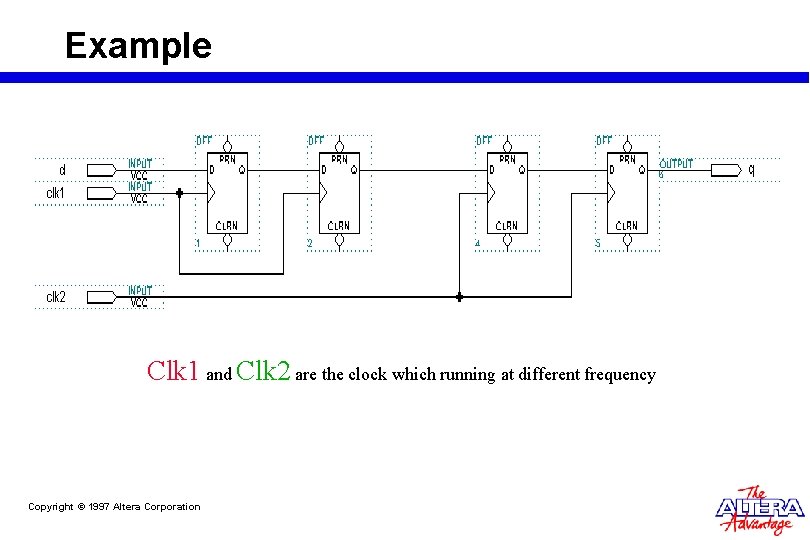
Example Clk 1 and Clk 2 are the clock which running at different frequency Copyright © 1997 Altera Corporation

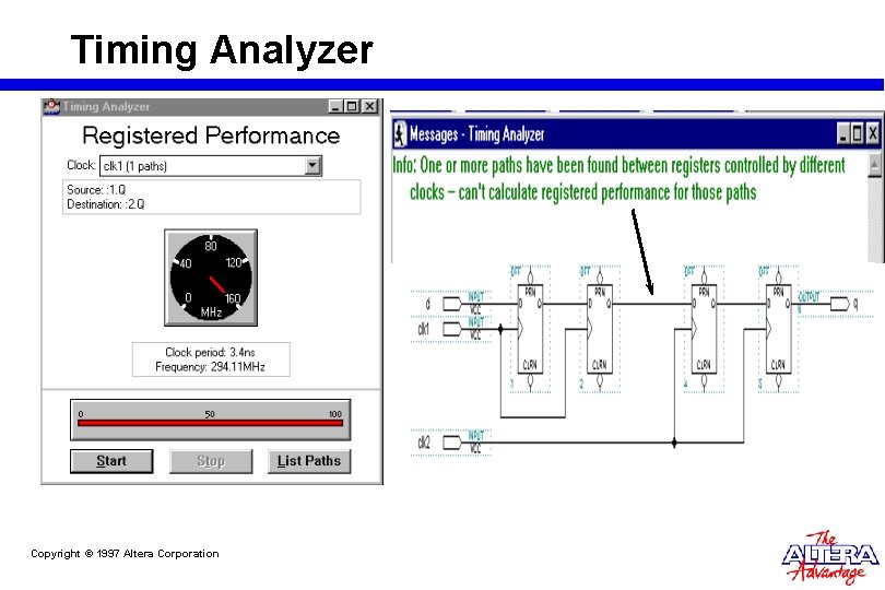
Timing Analyzer Copyright © 1997 Altera Corporation

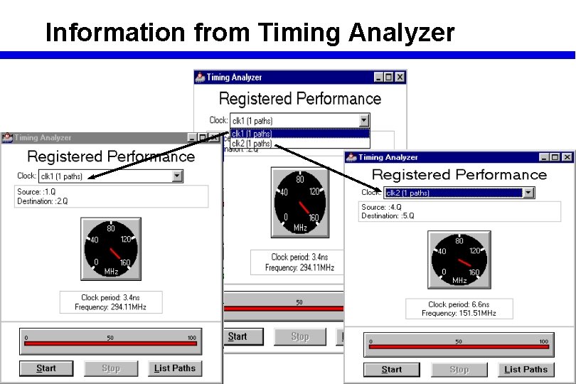
Information from Timing Analyzer Copyright © 1997 Altera Corporation

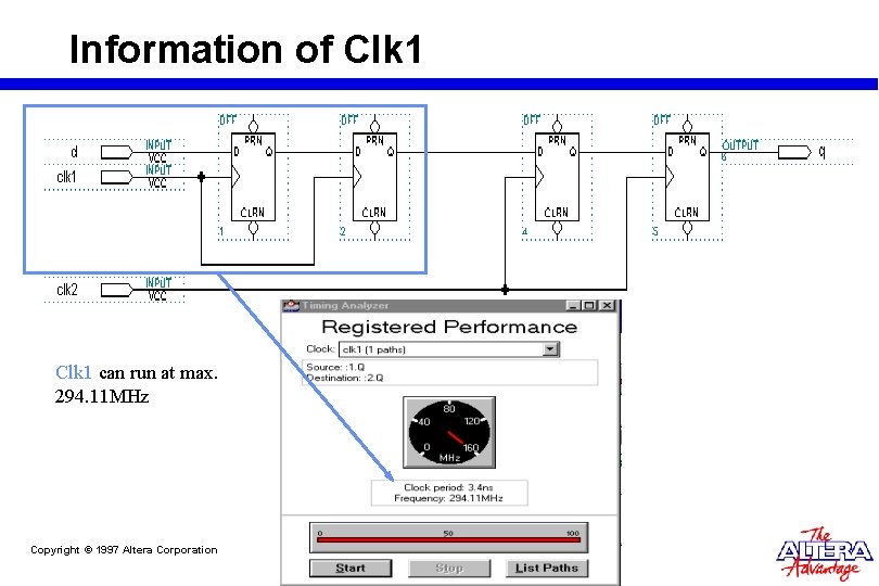
Information of Clk 1 can run at max. 294. 11 MHz Copyright © 1997 Altera Corporation

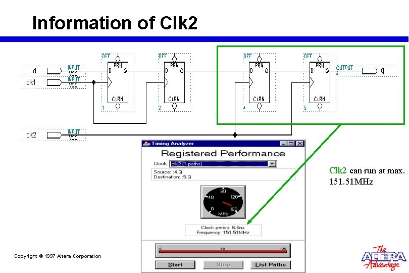
Information of Clk 2 can run at max. 151. 51 MHz Copyright © 1997 Altera Corporation

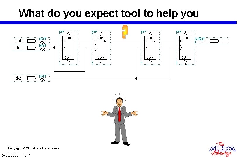
What do you expect tool to help you Copyright © 1997 Altera Corporation 9/10/2020 P. 7

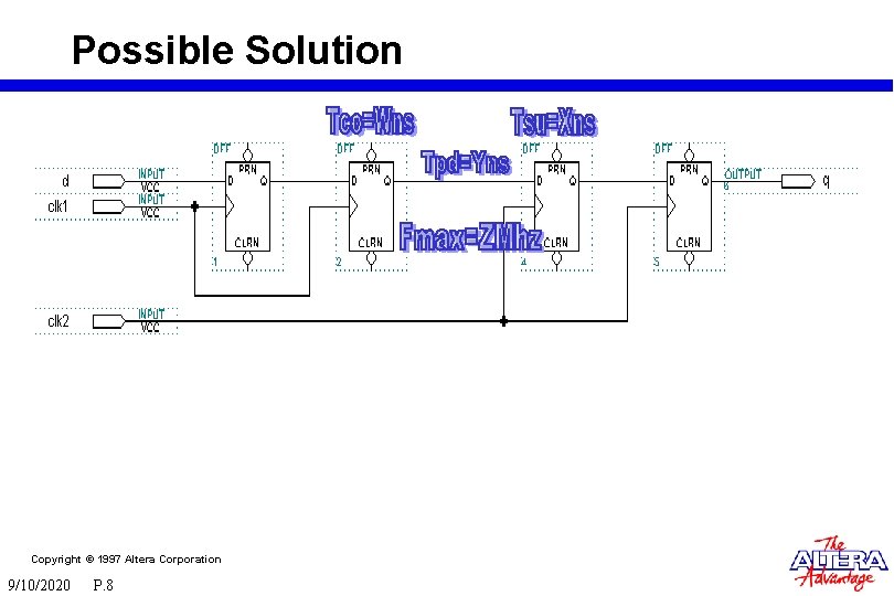
Possible Solution Copyright © 1997 Altera Corporation 9/10/2020 P. 8

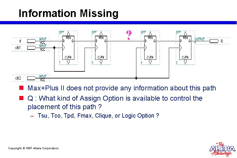
Information Missing ? n Max+Plus II does not provide any information about this path n Q : What kind of Assign Option is available to control the placement of this path ? – Tsu, Tco, Tpd, Fmax, Clique, or Logic Option ? Copyright © 1997 Altera Corporation

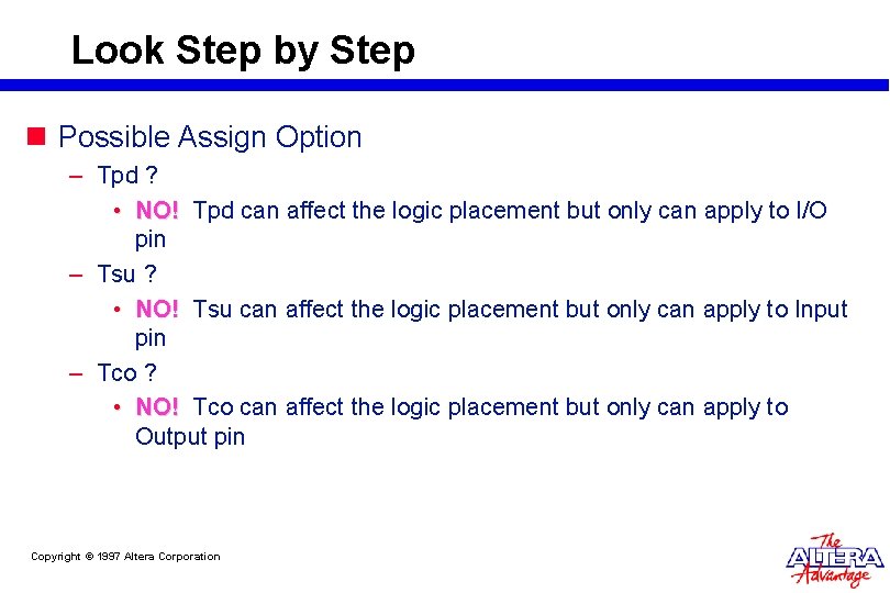
Look Step by Step n Possible Assign Option – Tpd ? • NO! Tpd can affect the logic placement but only can apply to I/O pin – Tsu ? • NO! Tsu can affect the logic placement but only can apply to Input pin – Tco ? • NO! Tco can affect the logic placement but only can apply to Output pin Copyright © 1997 Altera Corporation

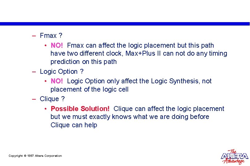
– Fmax ? • NO! Fmax can affect the logic placement but this path have two different clock, Max+Plus II can not do any timing prediction on this path – Logic Option ? • NO! Logic Option only affect the Logic Synthesis, not placement of the logic cell – Clique ? • Possible Solution! Clique can affect the logic placement but we must exactly knows what we are doing before Clique can help Copyright © 1997 Altera Corporation

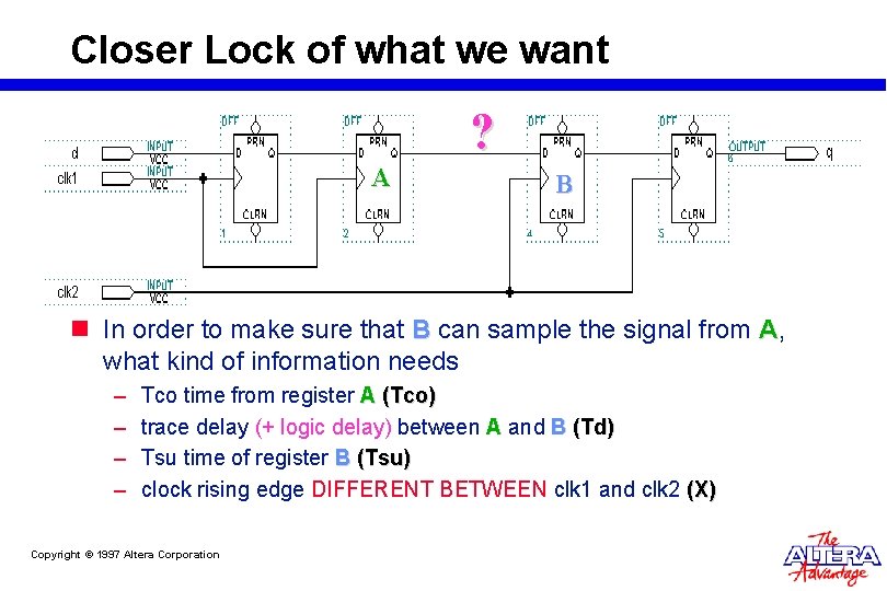
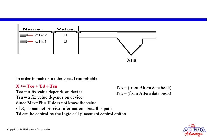
Closer Lock of what we want ? A B n In order to make sure that B can sample the signal from A, what kind of information needs – – Tco time from register A (Tco) trace delay (+ logic delay) between A and B (Td) Tsu time of register B (Tsu) clock rising edge DIFFERENT BETWEEN clk 1 and clk 2 (X) Copyright © 1997 Altera Corporation

Xns In order to make sure the circuit run reliable X >= Tco + Td + Tsu Tco = (from Altera data book) Tco = a fix value depends on device Tsu = (from Altera data book) Tsu = a fix value depends on device Since Max+Plus II does not know the value of X, so can not provide information about this path Td can be control by the logic cell placement control option Copyright © 1997 Altera Corporation

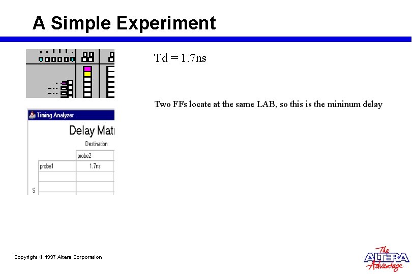
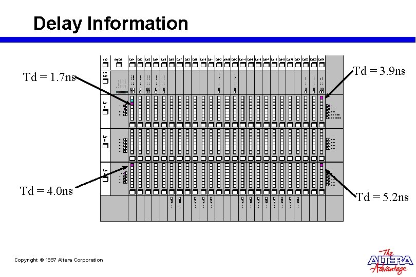
A Simple Experiment Td = 1. 7 ns Two FFs locate at the same LAB, so this is the mininum delay Copyright © 1997 Altera Corporation

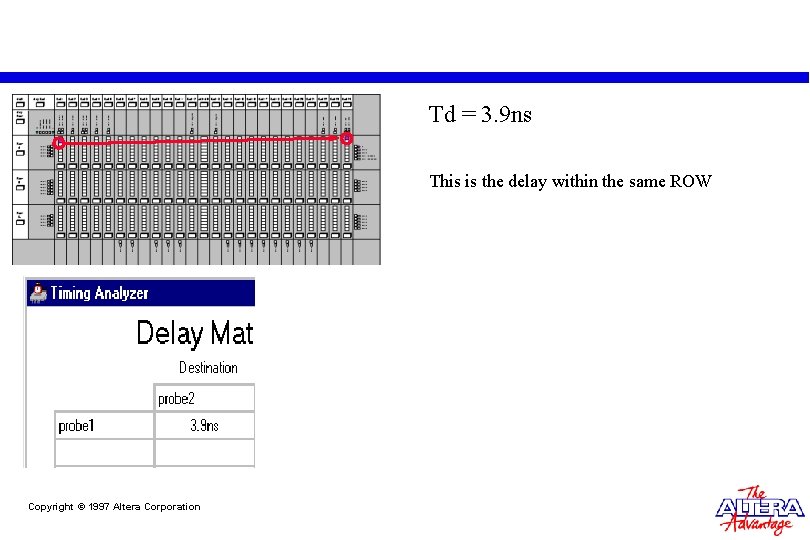
Td = 3. 9 ns This is the delay within the same ROW Copyright © 1997 Altera Corporation

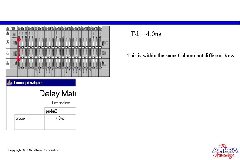
Td = 4. 0 ns This is within the same Column but different Row Copyright © 1997 Altera Corporation

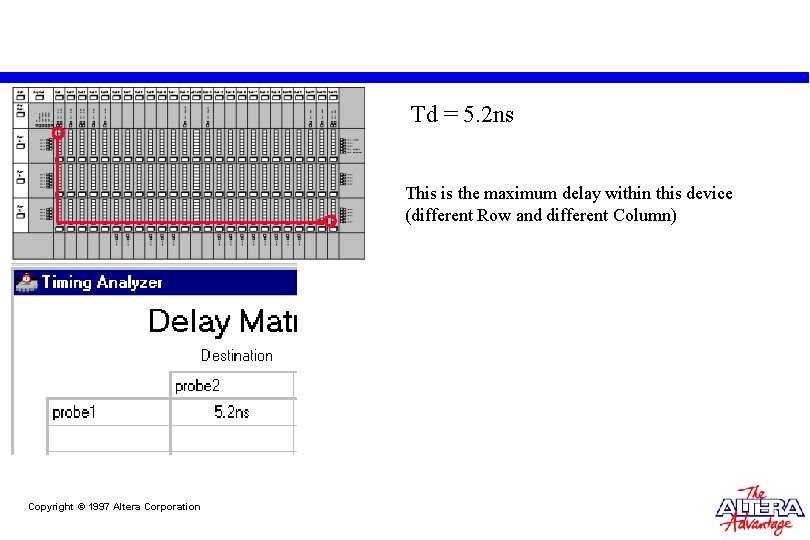
Td = 5. 2 ns This is the maximum delay within this device (different Row and different Column) Copyright © 1997 Altera Corporation

Delay Information Td = 1. 7 ns Td = 4. 0 ns Copyright © 1997 Altera Corporation Td = 3. 9 ns Td = 5. 2 ns

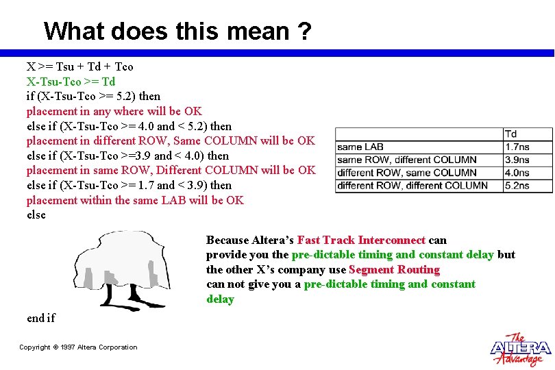
What does this mean ? X >= Tsu + Td + Tco X-Tsu-Tco >= Td if (X-Tsu-Tco >= 5. 2) then placement in any where will be OK else if (X-Tsu-Tco >= 4. 0 and < 5. 2) then placement in different ROW, Same COLUMN will be OK else if (X-Tsu-Tco >=3. 9 and < 4. 0) then placement in same ROW, Different COLUMN will be OK else if (X-Tsu-Tco >= 1. 7 and < 3. 9) then placement within the same LAB will be OK else Because Altera’s Fast Track Interconnect can provide you the pre-dictable timing and constant delay but the other X’s company use Segment Routing can not give you a pre-dictable timing and constant delay end if Copyright © 1997 Altera Corporation

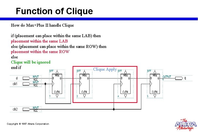
Function of Clique How do Max+Plus II handle Clique if (placement can place within the same LAB) then placement within the same LAB else (placement can place within the same ROW) then placement within the same ROW else Clique will be ignored end if Clique Apply Copyright © 1997 Altera Corporation

Max+Plus II Simulator n After the design, Max+Plus II Simulator can help you to find out the Tsu and Thold time problem Copyright © 1997 Altera Corporation

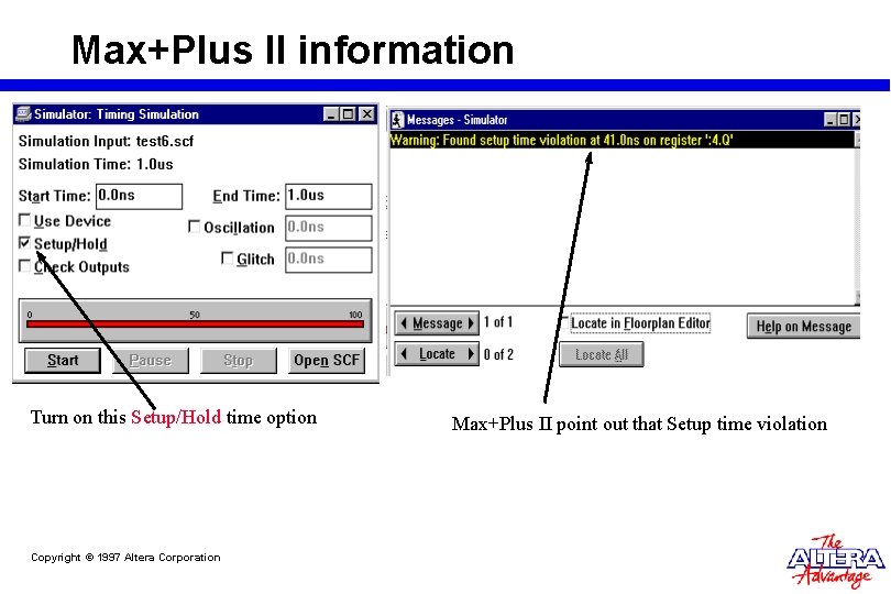
Max+Plus II information Turn on this Setup/Hold time option Copyright © 1997 Altera Corporation Max+Plus II point out that Setup time violation

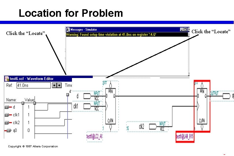
Location for Problem Click the “Locate” Copyright © 1997 Altera Corporation Click the “Locate”

Summary n Clique can help to make sure the multiple clock circuit running reliable if you really know what you want n Clique can use to force logic place within the same LAB or same ROW n Local Routing Option (for FLEX 6000 only) can use to force logic placement within the same LAB or Adjacent LAB Copyright © 1997 Altera Corporation

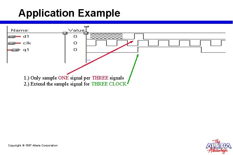
Application Example 1. ) Only sample ONE signal per THREE signals 2. ) Extend the sample signal for THREE CLOCK Copyright © 1997 Altera Corporation

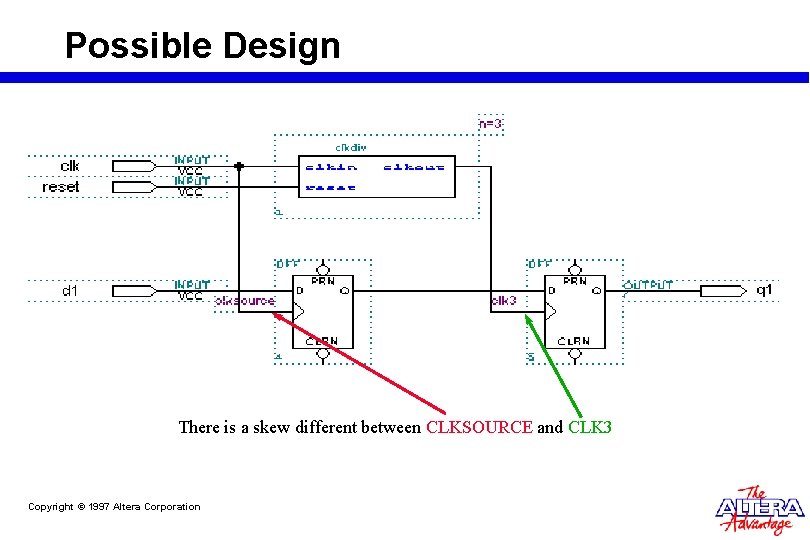
Possible Design There is a skew different between CLKSOURCE and CLK 3 Copyright © 1997 Altera Corporation

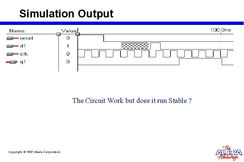
Simulation Output The Circuit Work but does it run Stable ? Copyright © 1997 Altera Corporation

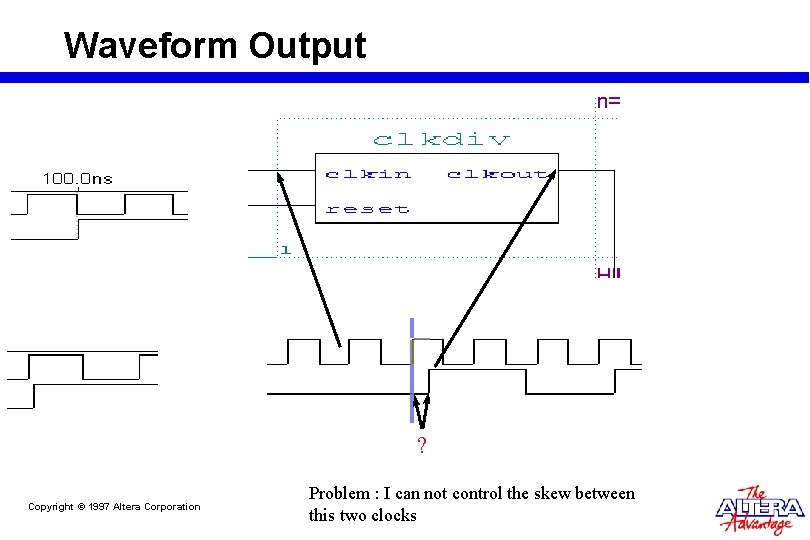
Waveform Output ? Copyright © 1997 Altera Corporation Problem : I can not control the skew between this two clocks

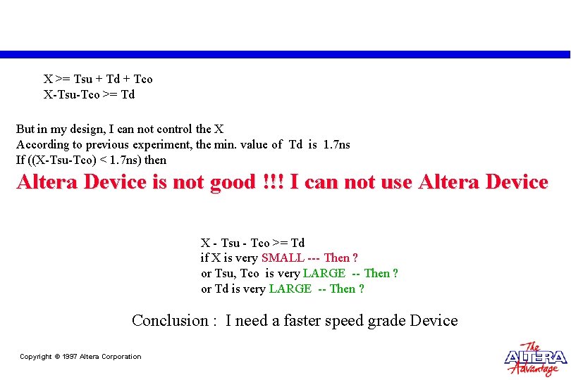
X >= Tsu + Td + Tco X-Tsu-Tco >= Td But in my design, I can not control the X According to previous experiment, the min. value of Td is 1. 7 ns If ((X-Tsu-Tco) < 1. 7 ns) then Altera Device is not good !!! I can not use Altera Device X - Tsu - Tco >= Td if X is very SMALL --- Then ? or Tsu, Tco is very LARGE -- Then ? or Td is very LARGE -- Then ? Conclusion : I need a faster speed grade Device Copyright © 1997 Altera Corporation

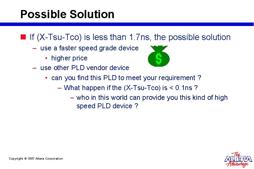
Possible Solution n If (X-Tsu-Tco) is less than 1. 7 ns, the possible solution – use a faster speed grade device • higher price – use other PLD vendor device • can you find this PLD to meet your requirement ? – What happen if the (X-Tsu-Tco) is < 0. 1 ns ? – who in this world can provide you this kind of high speed PLD device ? Copyright © 1997 Altera Corporation

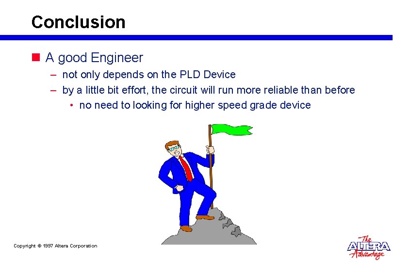
What is Engineer ? n If everytime having the problem, Engineer always use High Speed PLD device to solve the problem – everyone can be an engineer n A good Engineer when having problem, he will – chanallege himself instead of PLD device – that is the value of the engineer Copyright © 1997 Altera Corporation

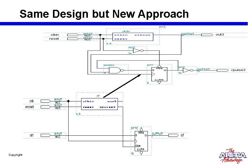
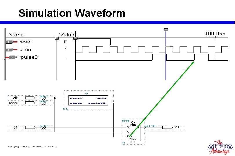
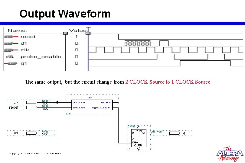
Same Design but New Approach Copyright © 1997 Altera Corporation

Simulation Waveform Copyright © 1997 Altera Corporation

Output Waveform The same output, but the circuit change from 2 CLOCK Source to 1 CLOCK Source Copyright © 1997 Altera Corporation

Conclusion n A good Engineer – not only depends on the PLD Device – by a little bit effort, the circuit will run more reliable than before • no need to looking for higher speed grade device Copyright © 1997 Altera Corporation