
Multilayer PCB Image Transfer Technology II Charles Kao
Multilayer PCB Image Transfer Technology II 高啟清博士 Charles Kao, Ph. D Tel: 02 -2601 -0700 Mobile: 0939 -268 -725 cckao@csun. com. tw V 2. 1 2007/4/10 2004/4/5 1/58

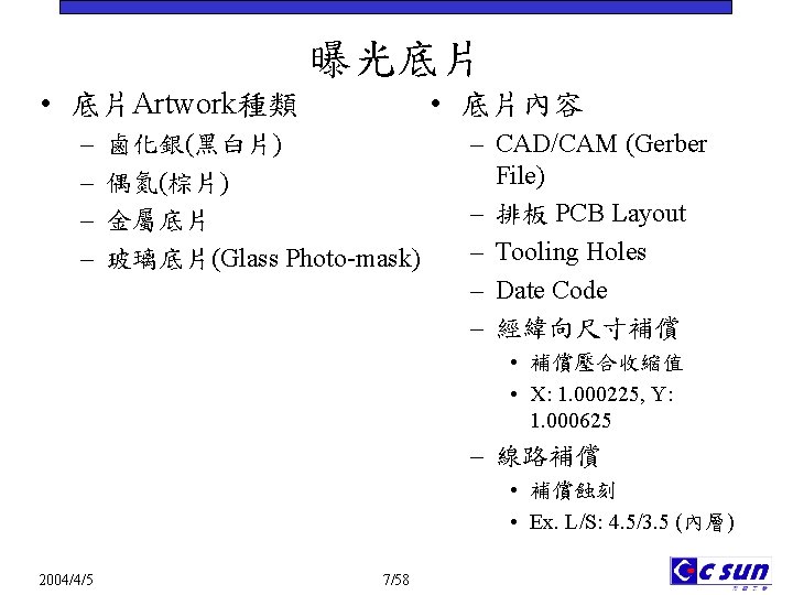
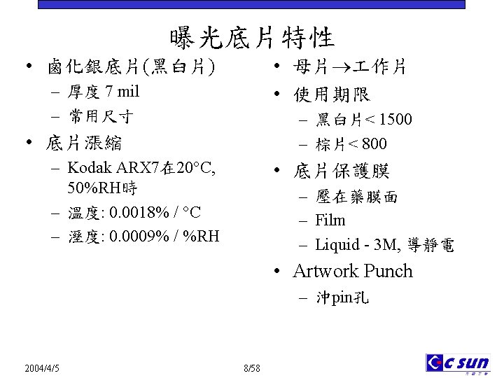
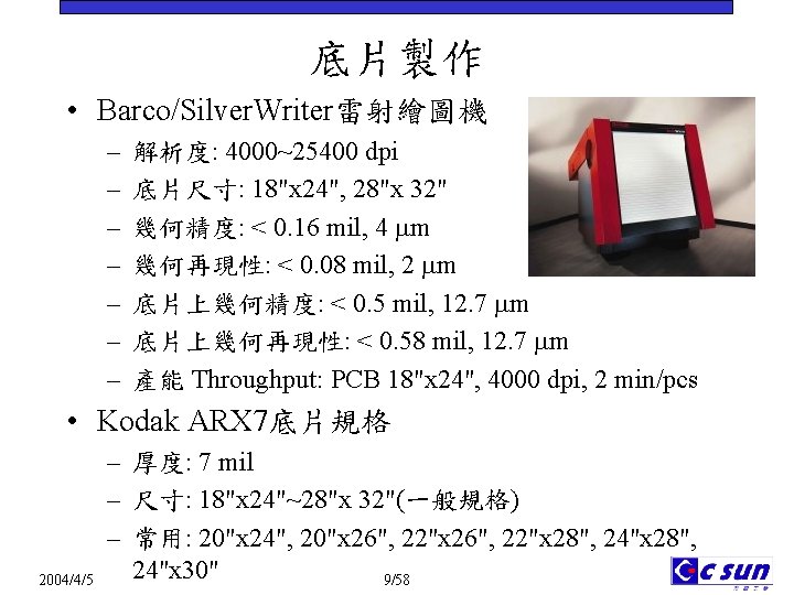
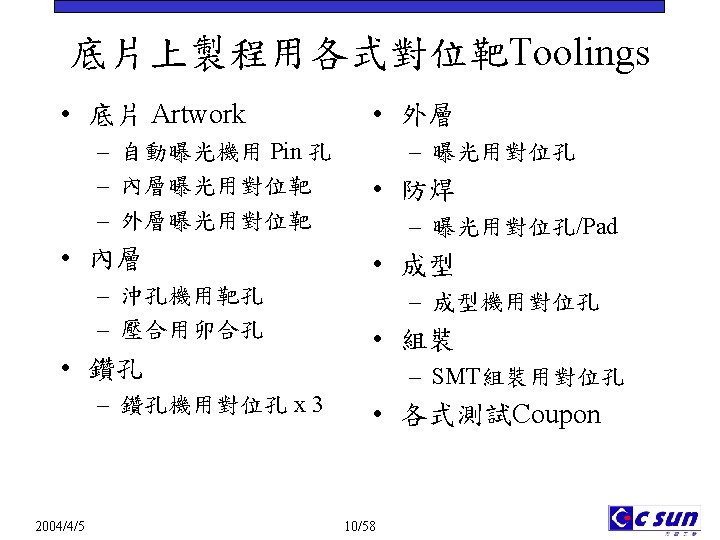
底片製作 • Barco/Silver. Writer雷射繪圖機 – – – – 解析度: 4000~25400 dpi 底片尺寸: 18"x 24", 28"x 32" 幾何精度: < 0. 16 mil, 4 m 幾何再現性: < 0. 08 mil, 2 m 底片上幾何精度: < 0. 5 mil, 12. 7 m 底片上幾何再現性: < 0. 58 mil, 12. 7 m 產能 Throughput: PCB 18"x 24", 4000 dpi, 2 min/pcs • Kodak ARX 7底片規格 2004/4/5 – 厚度: 7 mil – 尺寸: 18"x 24"~28"x 32"(一般規格) – 常用: 20"x 24", 20"x 26", 22"x 28", 24"x 30" 9/58
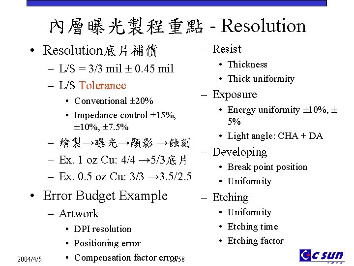
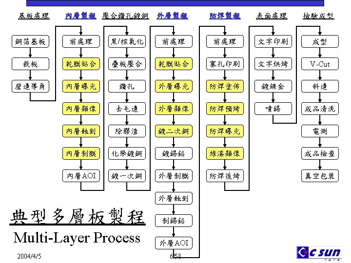
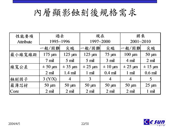
內層曝光製程重點 - Resolution • Resolution底片補償 – L/S = 3/3 mil 0. 45 mil – L/S Tolerance • Conventional 20% • Impedance control 15%, 10%, 7. 5% – Resist • Thickness • Thick uniformity – Exposure • Energy uniformity 10%, 5% • Light angle: CHA + DA – 繪製→曝光→顯影 →蝕刻 – Developing – Ex. 1 oz Cu: 4/4 → 5/3底片 • Break point position – Ex. 0. 5 oz Cu: 3/3 → 3. 5/2. 5 • Uniformity • Error Budget Example – Etching • Uniformity – Artwork 2004/4/5 • DPI resolution • Positioning error • Compensation factor error 15/58 • Etching time • Etching factor
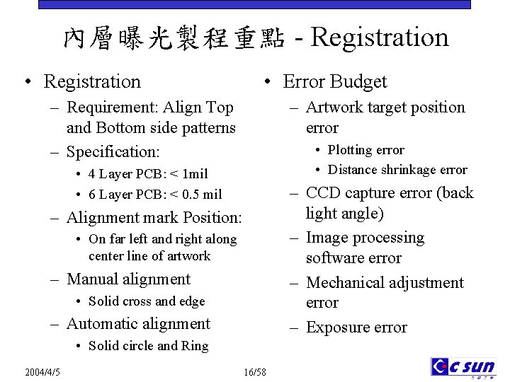
內層曝光製程重點 - Registration • Registration • Error Budget – Requirement: Align Top and Bottom side patterns – Specification: – Artwork target position error • Plotting error • Distance shrinkage error • 4 Layer PCB: < 1 mil • 6 Layer PCB: < 0. 5 mil – CCD capture error (back light angle) – Image processing software error – Mechanical adjustment error – Exposure error – Alignment mark Position: • On far left and right along center line of artwork – Manual alignment • Solid cross and edge – Automatic alignment • Solid circle and Ring 2004/4/5 16/58
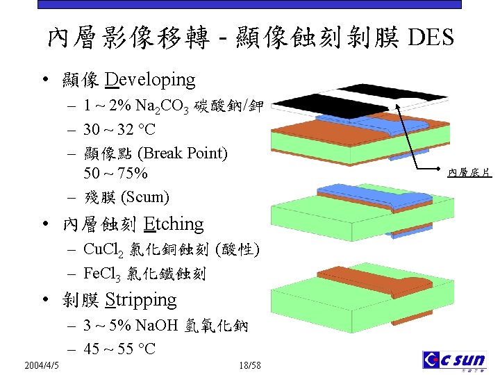
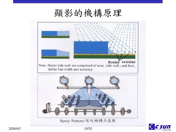

Etch Progression • Etch 3/3 on 1 oz Cu – Undercut = (R-T)/2 – Etch factor=2 t/(B-T) – Extent of etch = R/B 2004/4/5 20/58
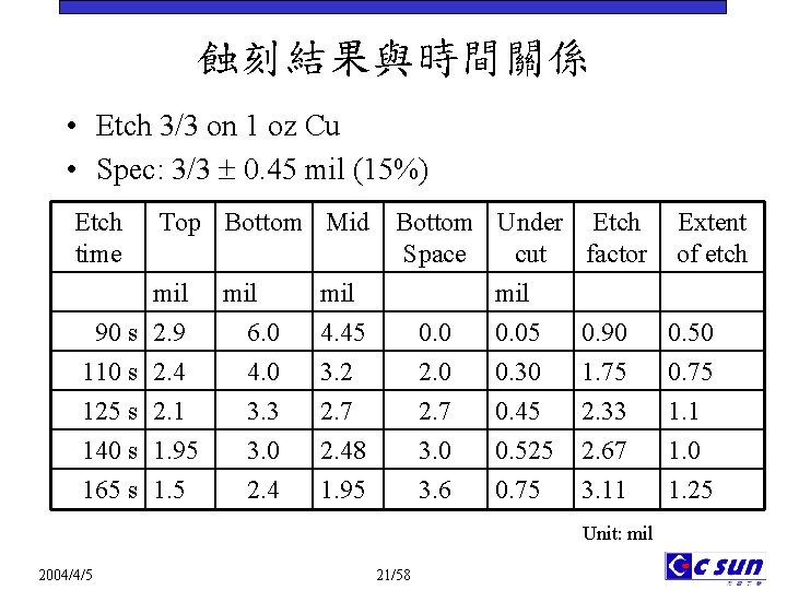
蝕刻結果與時間關係 • Etch 3/3 on 1 oz Cu • Spec: 3/3 0. 45 mil (15%) Etch time Top Bottom Mid Bottom Under Etch Space cut factor mil 90 s 2. 9 mil 6. 0 mil 4. 45 110 s 2. 4 125 s 2. 1 4. 0 3. 3 140 s 1. 95 165 s 1. 5 3. 0 2. 4 0. 0 mil 0. 05 0. 90 0. 50 3. 2 2. 7 2. 0 2. 7 0. 30 0. 45 1. 75 2. 33 0. 75 1. 1 2. 48 1. 95 3. 0 3. 6 0. 525 0. 75 2. 67 3. 11 1. 0 1. 25 Unit: mil 2004/4/5 Extent of etch 21/58
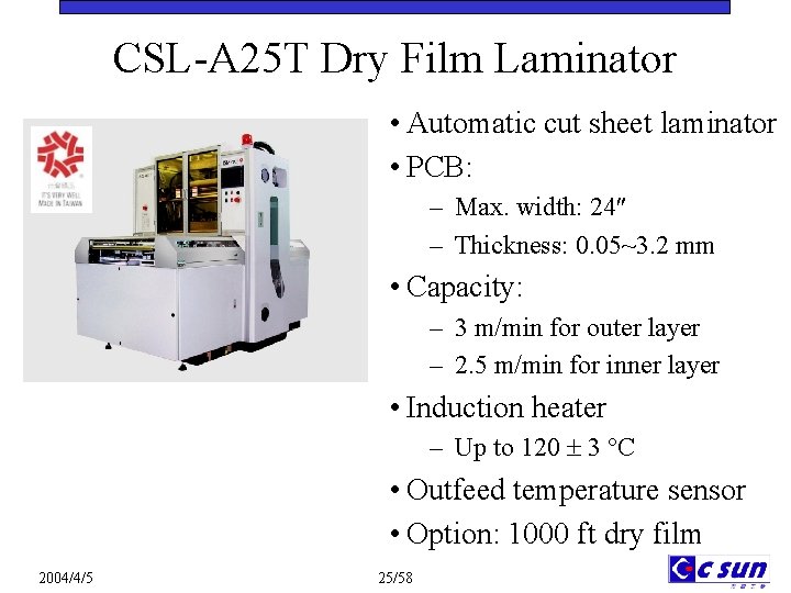
CSL-A 25 T Dry Film Laminator • Automatic cut sheet laminator • PCB: – Max. width: 24 – Thickness: 0. 05~3. 2 mm • Capacity: – 3 m/min for outer layer – 2. 5 m/min for inner layer • Induction heater – Up to 120 3 C • Outfeed temperature sensor • Option: 1000 ft dry film 2004/4/5 25/58
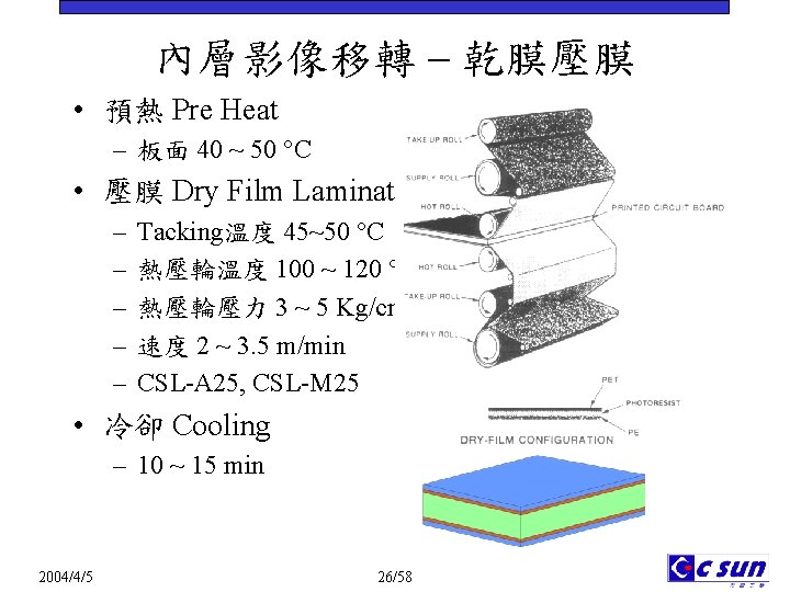
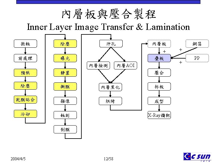
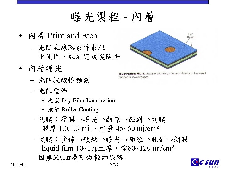
內層影像移轉 – 乾膜壓膜 • 預熱 Pre Heat – 板面 40 ~ 50 C • 壓膜 Dry Film Lamination – – – Tacking溫度 45~50 C 熱壓輪溫度 100 ~ 120 C 熱壓輪壓力 3 ~ 5 Kg/cm 2 速度 2 ~ 3. 5 m/min CSL-A 25, CSL-M 25 • 冷卻 Cooling – 10 ~ 15 min 2004/4/5 26/58
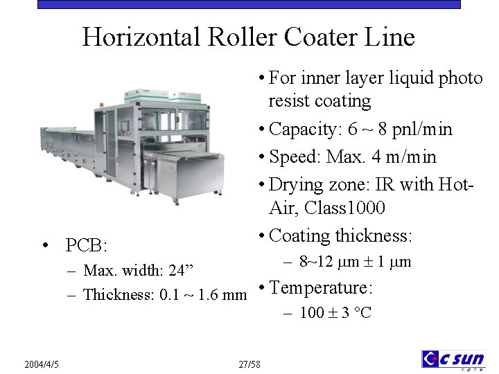
Horizontal Roller Coater Line • PCB: • For inner layer liquid photo resist coating • Capacity: 6 ~ 8 pnl/min • Speed: Max. 4 m/min • Drying zone: IR with Hot. Air, Class 1000 • Coating thickness: – 8~12 m 1 m – Max. width: 24” – Thickness: 0. 1 ~ 1. 6 mm • Temperature: – 100 3 C 2004/4/5 27/58
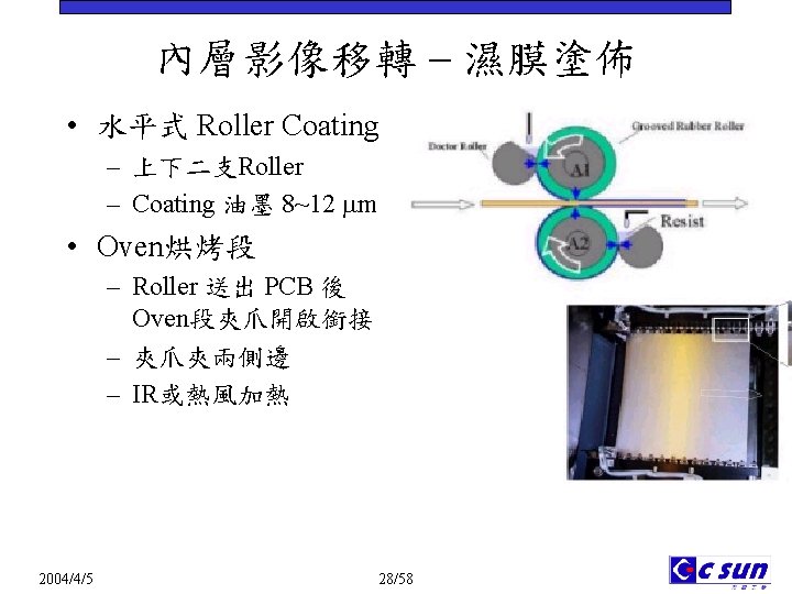
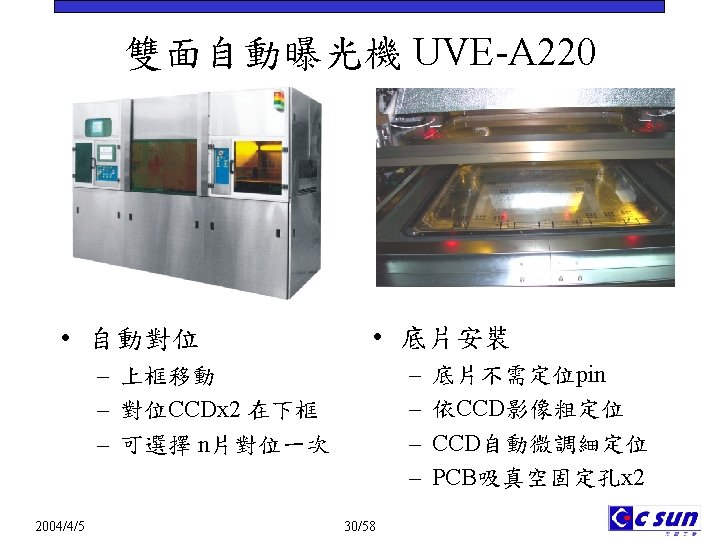
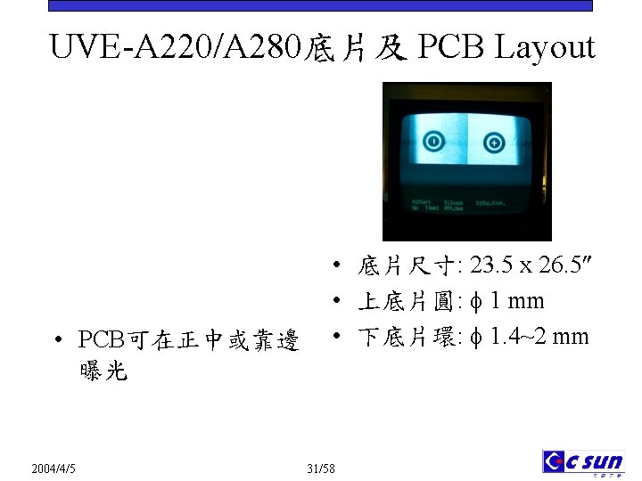
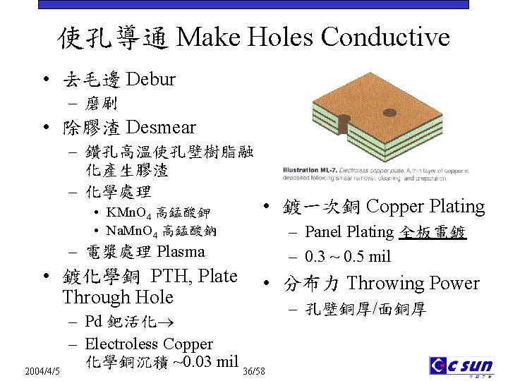
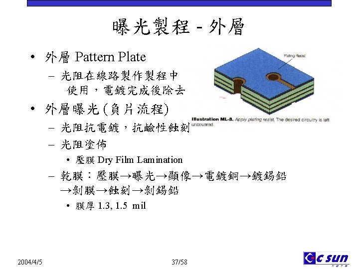
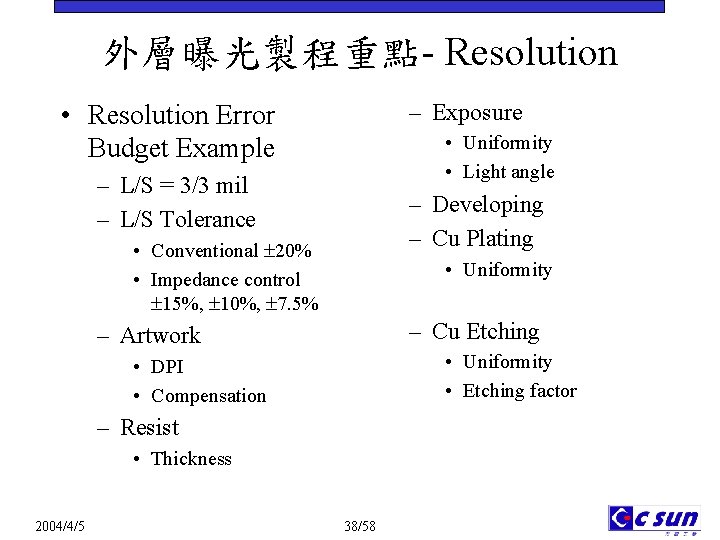
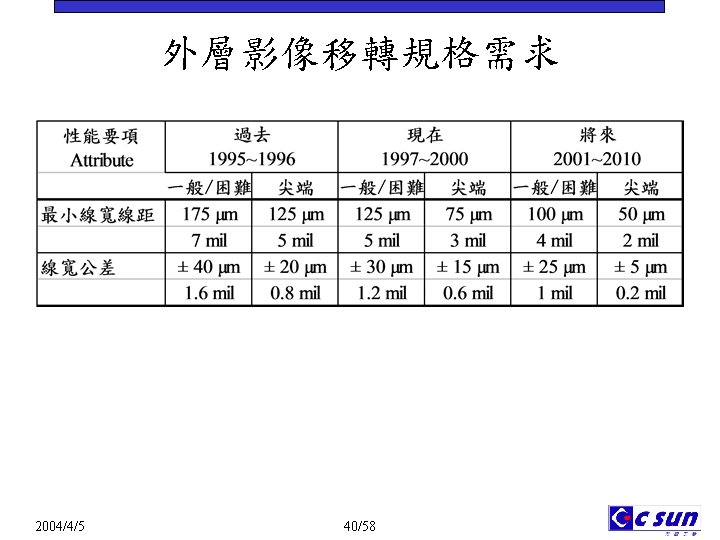
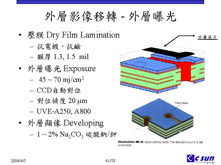
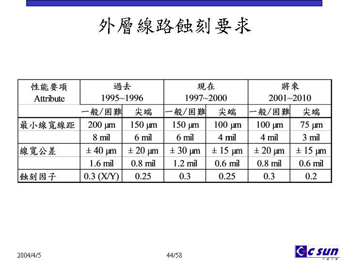
外層曝光製程重點- Resolution – Exposure • Resolution Error Budget Example • Uniformity • Light angle – L/S = 3/3 mil – L/S Tolerance – Developing – Cu Plating • Conventional 20% • Impedance control 15%, 10%, 7. 5% • Uniformity – Cu Etching – Artwork • Uniformity • Etching factor • DPI • Compensation – Resist • Thickness 2004/4/5 38/58
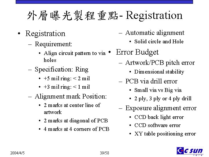
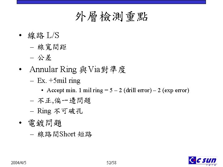
外層曝光製程重點- Registration – Automatic alignment • Registration • Solid circle and Hole – Requirement: • Align circuit pattern to via holes • Error Budget – Specification: Ring • Dimensional stability • +5 mil ring: < 2 mil • +3 mil ring: < 1 mil – PCB via drill error – Alignment mark Position: • 2 marks at center line of artwork • 2 marks at diagonal of PCB • 4 marks at 4 corners of PCB 2004/4/5 – Artwork/PCB pitch error 39/58 • Small via vs Big via • 2 ply, 3 ply or 4 ply drill – Exposure alignment error • CCD back light error • CCD software error • XY table positioning error
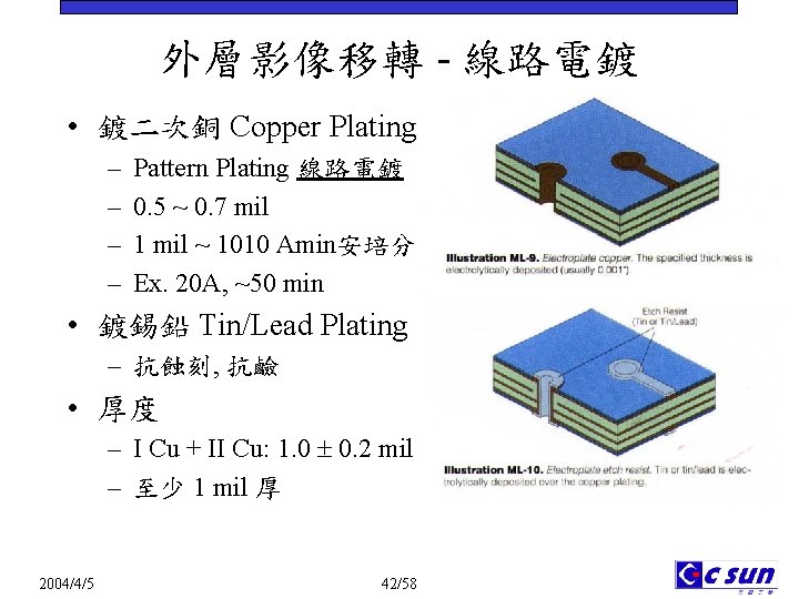
外層影像移轉 - 線路電鍍 • 鍍二次銅 Copper Plating – – Pattern Plating 線路電鍍 0. 5 ~ 0. 7 mil 1 mil ~ 1010 Amin安培分 Ex. 20 A, ~50 min • 鍍錫鉛 Tin/Lead Plating – 抗蝕刻, 抗鹼 • 厚度 – I Cu + II Cu: 1. 0 0. 2 mil – 至少 1 mil 厚 2004/4/5 42/58
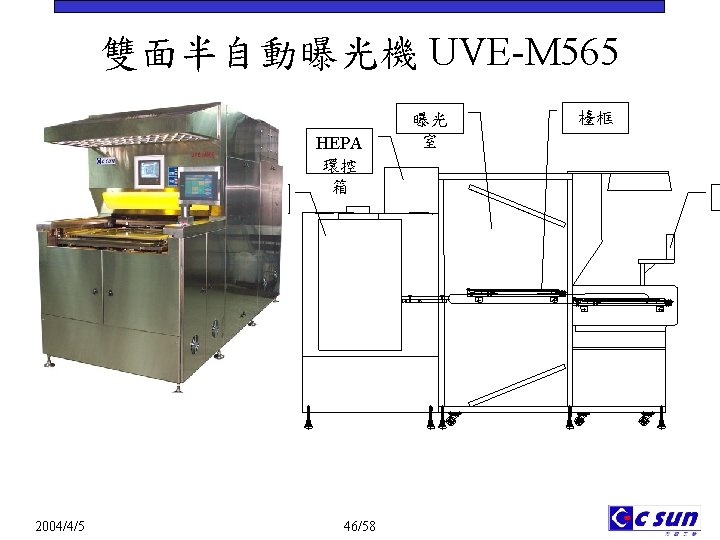
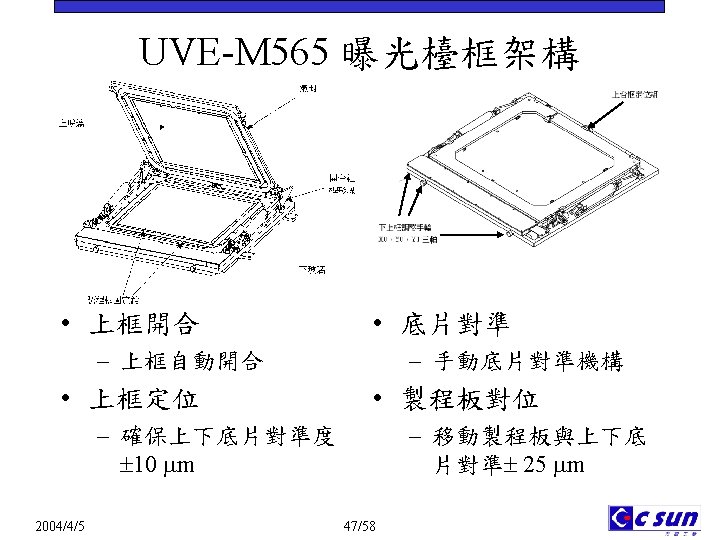
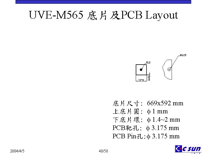
UVE-M 565 底片及PCB Layout 底片尺寸: 669 x 592 mm 上底片圓: 1 mm 下底片環: 1. 4~2 mm PCB靶孔: 3. 175 mm PCB Pin孔: 3. 175 mm 2004/4/5 48/58
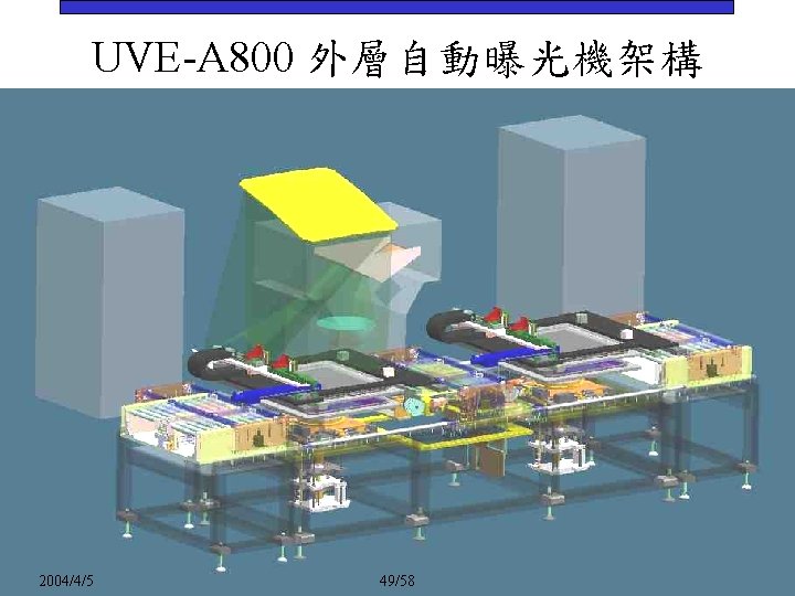
UVE-A 800 外層自動曝光機架構 2004/4/5 49/58
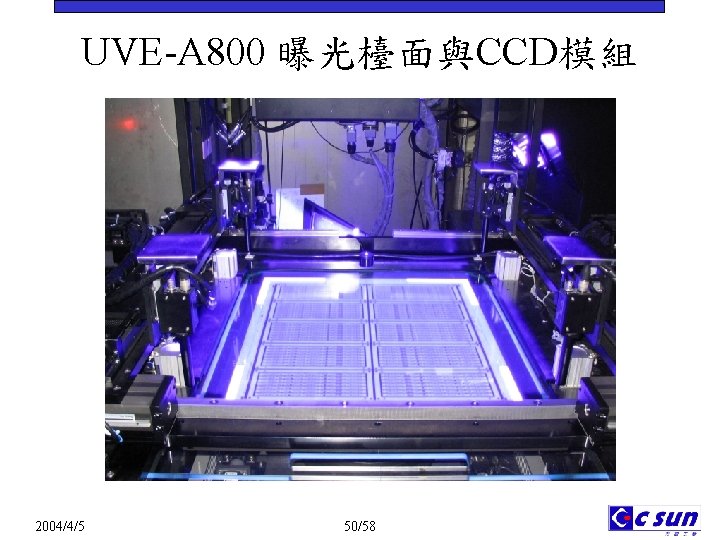
UVE-A 800 曝光檯面與CCD模組 2004/4/5 50/58
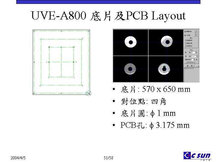
UVE-A 800 底片及PCB Layout • • 2004/4/5 51/58 底片: 570 x 650 mm 對位點: 四角 底片圓: 1 mm PCB孔: 3. 175 mm
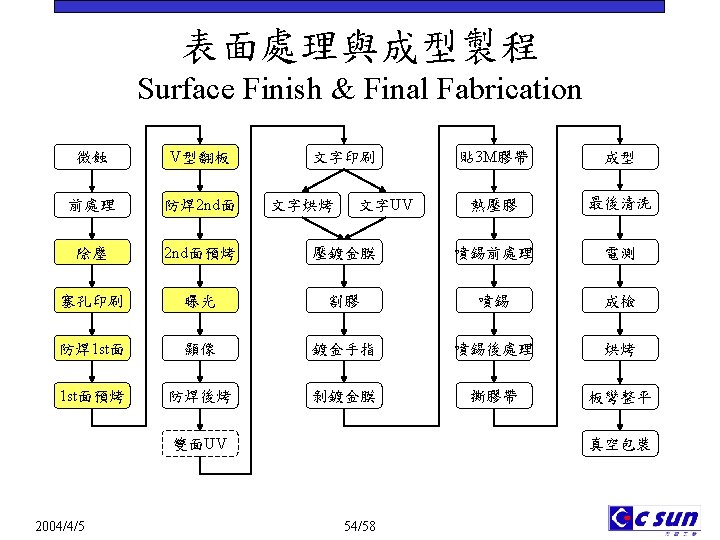
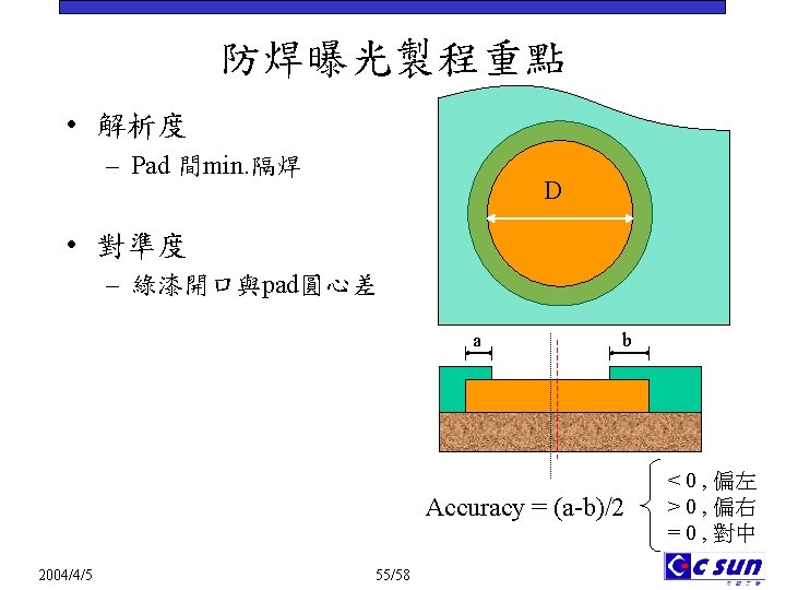

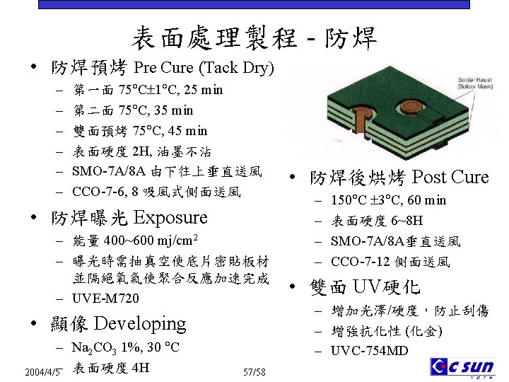
表面處理製程 - 防焊 SMOBC • 防焊 Solder Mask Over Bare Copper – 將板面除焊墊外區域以防焊油墨 覆蓋保護 – Post cure後厚度約0. 8 mil ↑ – Ex. 環單邊 + 4 mil • 液態感光防焊綠漆 Liquid Photoimageable Solder Mask – 塗佈→預烤→曝光 顯像→後烤→UV → • 防焊塗佈 – – 2004/4/5 網印 Screen Printing 簾塗 Curtain Coating 噴塗 Spray Coating 滾塗 Roller Coating 56/58
本單元結束 2004/4/5 59/58
- Slides: 58