MOSFET SCALING and Small Geometry Effects By Deepa

MOSFET SCALING and Small Geometry Effects By Deepa Asst. Professor Dept. of EIE SIT, Tumakuru

• Scaling: reduction of dimensions of MOSFET is called as scaling • Why scaling: design of high density chips in VLSI requires reduction in size of MOSFET

Types of scaling • There are two types of scaling 1. Full scaling / constant field scaling 2. Voltage scaling • Scaling factor: S>1 • Horizontal and vertical dimensions of large size transistors are scaled down by scaling factor.
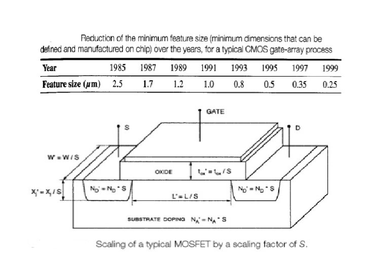
 • The dimensions of MOSFET scaled down by factor of")
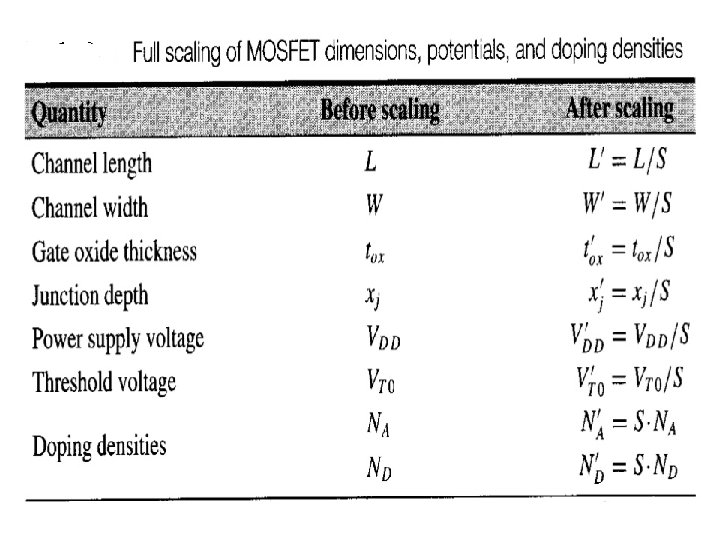
Full Scaling(Constant Field Scaling) • The dimensions of MOSFET scaled down by factor of S. • The magnitude of internal electric field is maintained constant. • All potentials are scaled down proportionally. • This potential scaling also effects Vt 0.
")
Full Scaling(Constant Field Scaling)
")
Full Scaling(Constant Field Scaling)

Advantages of Full Scaling • Significant reduction in power dissipation by S*S. • Cg is scaled down by S improves charge-up and charge down times. • Reductions of dimensions of MOSFET leads to reduction of parasitic capacitances and resistances

Disadvantage of Constant Field scaling Full scaling scales down the power supply and all terminal voltages proportionally but scaling of voltages may not be practical in some cases. Peripheral and interface circuitry may require certain voltage levels for all input and output voltages, which in turn would necessitate multiple supplies and complicated level shifters.

Constant voltage scaling • All dimensions of MOSFET are scaled down by factor of S • All supply and terminal voltages remain unchanged • Doping densities increased by factor of S*S Constant voltage scalingof MOSFET dimensions, potentials and doping densities

Constant voltage scaling

Constant voltage scaling

Constant voltage scaling Advantages: preffered over constant field scaling due to external voltage constraints Disadvntages : • Increases drain current density and power density by a factor of S*S*S. • Large increase in drain current density and power density may cause reliability issues like such as electro migration, hot-carrier degradation, oxide breakdown and electrical overstress.

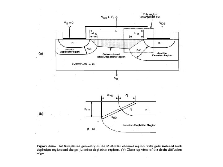
Short channel effects MOSFET is called short channel device if Channel length Leff = depletion region thickness of source and drain junctions x j. Short channel effects: 1. Limitations will be on electron drift characteristics in channel 2. Modification of Vt due to shortening of channel length

Short channel effects • Ey along the channel increases as channel length is reduced • Vd α Ey for lower value of Ey • For higher channel Ey= 10^5 V/cm Vd in channel saturation value=10^7 cm/s • Velocity saturation has significant effect on I-V characteristics

Short channel effects ID due to short channel effect

Short channel effects • In short channel surface mobility α Ex • Surface mobility is reduced w. r. t bulk mobility since Ey influences scattering of carriers in surface • Surface electron mobility can be expressed as

Short channel effects

Modification of Vt due to Short channel effects • In long channel MOSFET, channel depletion region is assumed to be created by VGS, with S & D depletion regions neglected. • Shape of gate induced bulk depletion region was assumed to be rectangular extending from source to drain
- Slides: 21