More Wave Equation Solutions Leading To Energy Bands

More Wave Equation Solutions Leading To Energy Bands 2 and 4 February 2015
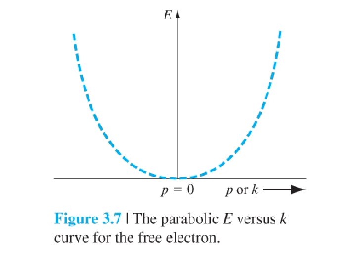
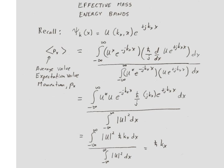
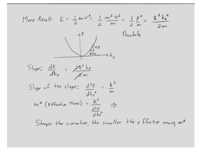

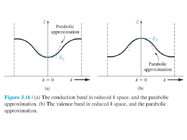
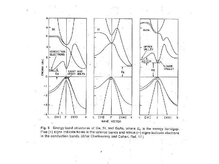
Electron Effective Mass For electrons in semiconductor lattice, Analogy to free electron, and, Free electron mass For example, in Si in Ga. As, The bottom part of conduction band can be approximated by the parabola. 15

Conduction Band Valence Band E For valence band holes Ec Ev k For conduction band electrons E Bandgap 17
 Conduction band Filled with few electrons Eg")
Band Structure of Insulators Conduction band (empty) Conduction band Filled with few electrons Eg Eg Valence band (full) Filled with few holes Valence band T=0 K T>0 K Few number of electrons and holes results in poor conductivity 21
 Conduction Filled with some electrons band Eg")
Band Structure of Semiconductors Conduction band (empty) Conduction Filled with some electrons band Eg Valence band (full) Eg Filled with some holes Valence band T=0 K T>0 K Significant number of electrons and holes results in higher conductivity than insulator 22

Band Structure of Metals Empty band Band overlap Occupied band T=0 K It is easy for the electrons to jump into the empty levels, so metals have high conductivity. 23

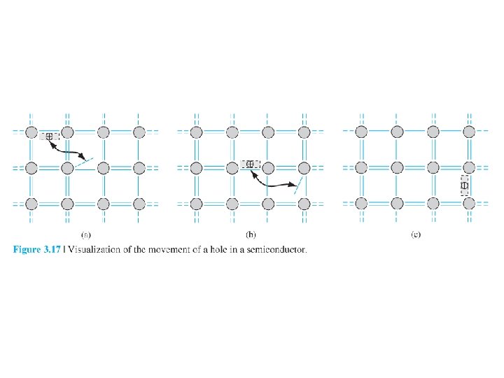
Concept of Hole • The movement of a valence electron into a empty state is equivalent to the movement of the positively charged empty state itself • Movement of holes can also give rise to a current • Each hole carries 1. 6 Х 10 -19 (C) of charge 24
- Slides: 27