More than Moore how much more Fifty years


- Slides: 25
More than Moore, how much more? Fifty years of Moore’s Law József Gyulai Professor Emeritus Chair Electronic Devices, BME-BUTE, Inst. Tech. Phys. & Matl. Sci. , MFA
Nobel prizes – near microelectronics Nobel Committee considers usefulness J. Bardeen, W. H. Brattain, W. Shockley, transistor (1956) L. Esaki, I. Giaever, B. D. Josephson, application of tunneling (1973) K. von Klitzing, quantum Hall-effect (1985) E. Ruska electron microscope, G. Binnig, H. Rohrer tunnel microscope (1986) Z. I. Alferov, semiconductor laser, H. Kroemer, UHF transistor, optics, J. S. Kilby, integrated circuit (2000) W. S. Boyle, G. E. Smith, CCD optics, Charles K. Kao, optical fiber (2009) A. Geim, K. Novoselov, graphene (2010) N, Shuji, A. Hiroshi and A. Isamu, blue LED diode Geim was awarded in 2000 with shared Ig. Nobel prize Ig. Nobel: “first make people laugh, then make them think”: diamagnetic levitation 1 T- 10 T field is enough for levitation of living bodies
Miniaturization • Key to success of microelectronics was that “scale down”: worked: transistor with shrunk dimensions possess the same characteristics except for heat dissipation. . . • As fringe benefit, smaller sizes brought not only portability, even wearebility, less power consumption, but also increased reliability: • amount of intelligence stacked into the device added to reliability • A good figure of merit is one mistake for 1010 steps, which with added redundant organization can still be improved.
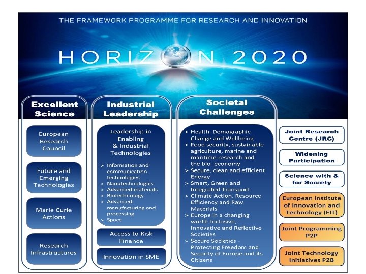
”Moore’s Law” • “Doubling the number of elements on the chip yearly”. . . “may work till end of the seventies…” – says Gordon Moore (Electronics, 38(8), apr. 19, 1965) • We may say that this is a generic law, which is more a law of economy than that of technology – production only satisfies market demands! • International Technology Roadmap for Semiconductors, ITRS: http: //public. itrs. net/ a four-yearly study with biannual corrections
”Moore’s Law” in my past, develop ionimplantation to technology • Too early patent of W. Shockley became a fortune globally: when the need for the technique became general, the patent was worn out (17 years passed). . . • My first postdoc stay at Caltech (1969 -70) was preceded just by one year, when Intel (Moore, Noyce, Deal, Grove, Vadasz. . . ) left Fairchild – the company supplying the forming Mayer group, including me • Intel’s start-up success was a simple trick. They were first to produce logic gates on a single chip • The early success was the cause that the young Intel refused to apply ion implantation as we argued at the 1 st Conf. on Implantation (Thousand Oaks, CA, 1970). • In the coming decade, the Mayer-Gyulai (Caltech) group contributed that ion implantation became a crucial technology (pre-amorphization technique)
”Moore’s Law” • First: National Technology Roadmap for Semiconductors – determine developments enabling fulfillment of ”Moore’s Law” • Later changed to ”International Technology Roadmap for Semiconductors, ITRS: http: //public. itrs. net/ – a four-yearly study with biannual corrections • Now, expanded, deals not only with memories and processors, but with tools for telecommunication (high frequency, optical, etc. ) and portability
An example from ITRS: Difficult technology tasks, 2011: black Yellow “known by industry”, “needs development” , white “no known solution”, “red brick wall” – to date always found solution. . . (PROCESS INTEGRATION, DEVICES, AND STRUCTURES
Success of ITRS on 2010 issue, http: //public. itrs. net/ How long will this work?
More than Moore, how much more? Another, recent example from ITRS: Difficult technology tasks, 2013: (Lithography challenges)
Intel processor using 14 nm technology - instead of 2022 news of the day
Moore’s Law today • Moore’s Law is a ”law” more of economics than of technology – proof are present investments into post-Moore solutions • Mark Bohr, Intel's director of process architecture and integration: ”Moore’s Law in its original form is dead, since a decade”. • In its original coverage, yes, but • Scale down may work till 2020, but question goes not only for memories and processor, but for telecommunication, etc. , too. Go to 3 D, optics, spintronics, etc. (Graphs from ENIAC project)
Non-volatile memory forecast • Going 3 D, i. e. , to stacked structures, NAND and NOR Flash memory, scaling down to 12 nm half-pitch looks straightforward till 2028 • Research is needed for magnetic/spin torque and for resistive devices • Reliability issue is difficult because of complex structure: failure mechanisms are very different for transistors, for interconnects, etc. May lead e. g. , to need of optical or carbon based interconnects
Hot areas in our field • Computer in telecommunication – – Mobile devices Wear-on devices Ambience intelligence (intelligent car, intelligent “mote”) Acoustic devices • “Revolution” of sensors and coupled actuators – Can be biomaterial, too… – Automation of transport • Micro- és nanotechnology – „Energy harvesting” • “Revolution” of lighting – Light emitting diode (LED), Organic LED • Priorities in EU: – „Energy efficient buildings”, – „Green car”, – „Factory of the future”
ITRS Roadmap 2013 Conclusions • • • “First of all, the aggressive bi-annual introduction of new semiconductor technologies allowed ICs, consisting of even hundreds of million of transistors, to be produced cost effectively. This made it possible to integrate extremely complex systems on a single die or in a single package at very attractive prices. Furthermore, progress in packaging technology enabled the placement of multiple dies within a single package. These categories of devices are defined as system on chip (SOC) and system in package (SIP). Second, manufacturers of integrated circuits offering foundry services were able to provide, once again, the “New ASICs” at very attractive costs. This led to the emergence of a very profitable business for design “only” houses, i. e. , companies that do not manufacture ICs themselves, but produce the designs that are manufactured elsewhere. Third, development of sophisticated equipment for advanced integrated circuits proliferated to adjacent technology fields and by so doing the realization of flat panel displays (FPD), MEMS sensors, radios and passives, etc. , was made possible at reasonable costs. Under these conditions system integrators were once again in the position to fully control system design and product integration. “
Nanoelectronics • Scale down cannot go ‘ad infinitum’, new solutions are needed (<14 nm node): • Smart cut© - “peel” bulk semiconductor materials, like were mica, to make nearly 2 D substrates, for SOI wafers. . . • New materials for channel, higher mobility than that of Si: – Six Ge 1 -x – In. Ga. As (L. Czornomaz: Comp. Semicond, 1/2014, 32) – Graphene? Lithography solutions by the Biró group
Some expectations • The other day in a class on monolythic IC technology, I was mumbling if the topic will have importance in post-Moore times • I think, it will, as it represents a basic technical knowhow necessary even in biotech applications
Hope for future of Moore’s law and potential proof for its economic nature • What I feel crucial is that new solutions in the nanometer region will or will not be able to satisfy reliability issues • E. g. , if biomolecules come in play, will the rather exact electronic reliability issue merge with redundancy-operated ‘reliability’ of biosystems? • How close can we go to the k. T-limit? • I expect that once in the future, when we’ll have whatever, e. g. , biocomputers, then will come an engineer, who for fun determines the gate level equivalent circuit for that device • and he’ll find that the exponential law remained valid. . .
TRL: Technology readiness level
Future of nanoelectronics • In my view, only solutions will ‘make it’ which fit into today’s foundries, albeit with slight modifications • New solutions needed because of scale down limitations: – Instead of electron conduction, other binary systems, e. g. , shift register using spin, ~tronics (D. Jamieson, Melbourne) – Optical data transport on chip instead of metallization – inevitable – Optics: plasmonics? – Analog vs digital systems – So-called biomimetic solutions Insulator 28 Si Substrate
Quantumcomputer solutions “Qubit” denotes entangled particles, e. g. , seven qubit of 5 fluorine and 2 carbon can factorize 15: 3 ٠ 5=15 Radio waves trigger and NMR reads out the result 2012: Superconductiong stabilization (10 μs) of qubit using silicon technology! IBM Research Dicarbonylcyclopentadi enyl (perfluorobutadien -2 -yl) iron (C 11 H 5 F 5 O 2 Fe ) (ill. pentafluorobutadienyl cyclopentadienyldicarb onyl-iron complex)
Vision • 20 th century almost erased border between physics and chemistry, • In the 21 st, I’m expecting this to happen towards biology • Arsenal of mathematics is improving simultaneously allowing ‘quasi-exact’ solutions to problems
„Ceterum censeo. . . ”: • Science and technology of today can only have one mission and maybe two main directions – corresponding somehow to preservation of self and of the race: 1. Search ways, modes whether, and if positive, on what technical level can 8 – 10 billion people live on Earth in kind of symbiosis with other forms of life? … 2. Extension of life span of individuals attracts great interest – causing unheard-of development of biological science If ‘recipes’ become known, will society absorb them and put into action in time?
Buckminster Fuller, architect and one of Club of Rome founders: Operating Manual for Spaceship Earth - (1969) “…One outstandingly important fact regarding Spaceship Earth, and that is that no instruction book came with it…„ Biosphere, Montreal, 1967 Recyling economy – when? Fullerenes
Thank you for your attention