Monolithic active pixel sensor for ionizing radiation using
![Introduction STAR ILC ALICE-LHC ATLAS Requirements for inner pixel layers STAR ALICE-LHC Timing [ns] Introduction STAR ILC ALICE-LHC ATLAS Requirements for inner pixel layers STAR ALICE-LHC Timing [ns]](https://slidetodoc.com/presentation_image/1e08135608e12a733ac1c85b63f340d3/image-3.jpg)
![Depletion Width [µm] Depletion Width in Silicon 150 1000 Ohm-cm 100 Ohm-cm 50 0 Depletion Width [µm] Depletion Width in Silicon 150 1000 Ohm-cm 100 Ohm-cm 50 0](https://slidetodoc.com/presentation_image/1e08135608e12a733ac1c85b63f340d3/image-16.jpg)
- Slides: 32

Monolithic active pixel sensor for ionizing radiation using 180 nm HV-SOI process Tomasz Hemperek, Tetsuichi Kishishita, Hans Krüger, hemperek@uni-bonn. de RESMDD 14 - 09. 10. 2014

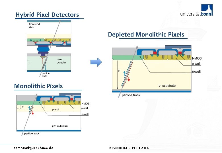
Hybrid Pixel Detectors Depleted Monolithic Pixels hemperek@uni-bonn. de RESMDD 14 - 09. 10. 2014
![Introduction STAR ILC ALICELHC ATLAS Requirements for inner pixel layers STAR ALICELHC Timing ns Introduction STAR ILC ALICE-LHC ATLAS Requirements for inner pixel layers STAR ALICE-LHC Timing [ns]](https://slidetodoc.com/presentation_image/1e08135608e12a733ac1c85b63f340d3/image-3.jpg)
Introduction STAR ILC ALICE-LHC ATLAS Requirements for inner pixel layers STAR ALICE-LHC Timing [ns] 200 000 20 000 Particle Rate [k. Hz/mm 2] M 100 10 250 1000 Fluence [neq/cm 2] > 1012 > 1013 1012 2 x 10¹⁵ Ion. Dose [Mrad] > 0. 3 0. 7 0. 4 80 hemperek@uni-bonn. de ILC S 350 O M C c i h t i l o on ATLAS-LHC ATLAS-HL-LHC 25 25 RESMDD 14 - 09. 10. 2014 ? 10000 2 x 10¹⁶ - 2 x 10¹⁵ >500 - 100

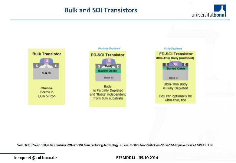
Bulk and SOI Transistors From: http: //news. softpedia. com/news/28 -nm-SOI-Manufacturing-Technology-is-Here-to-Stay-Soon-Will-Show-50 -to-550 -Improvements-266092. shtml hemperek@uni-bonn. de RESMDD 14 - 09. 10. 2014

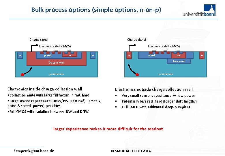
Bulk process options (simple options, n-on-p) Charge signal Electronics (full CMOS) p-well P+ nw Electronics (full CMOS) P+ p-well n+ nw deep p-well Deep n-well - p-substrate Electronics inside charge collection well Electronics outside charge collection well §Collection node with large fill factor rad. hard §Large sensor capacitance (DNW/PW junction!) x-talk, noise & speed (power) penalties §Full CMOS with isolation between NW and DNW § § § Very small sensor capacitance low power Potentially less rad. hard (longer drift lengths) Full CMOS with additional deep-p implant larger capacitance makes it more difficult for the readout hemperek@uni-bonn. de RESMDD 14 - 09. 10. 2014 n+

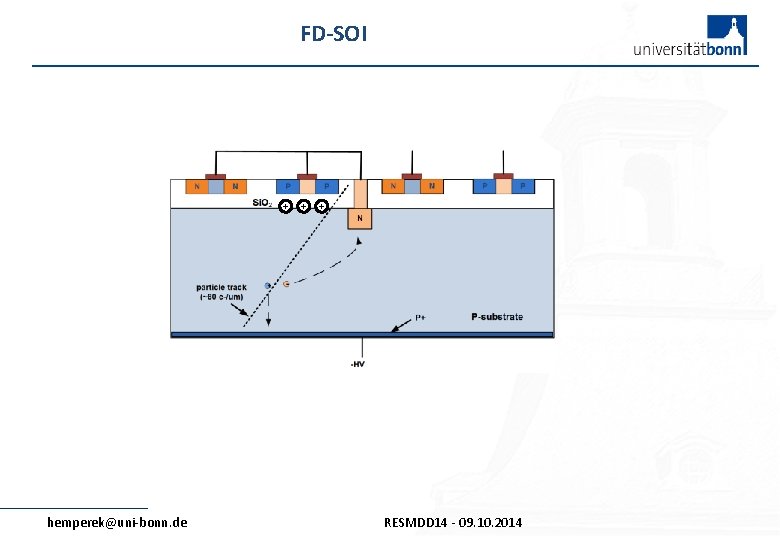
FD-SOI + + + CHANGE hemperek@uni-bonn. de RESMDD 14 - 09. 10. 2014

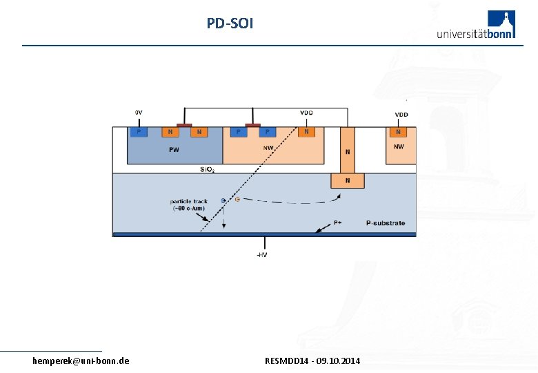
PD-SOI hemperek@uni-bonn. de RESMDD 14 - 09. 10. 2014

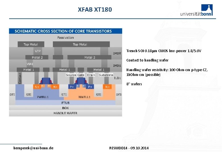
XFAB XT 180 Trench SOI 0. 18µm CMOS low-power 1. 8/5. 0 V Contact to handling wafer Handling wafer resistivity: 100 Ohm-cm p-type CZ, 1 k. Ohm-cm (possible) 8” wafers hemperek@uni-bonn. de RESMDD 14 - 09. 10. 2014

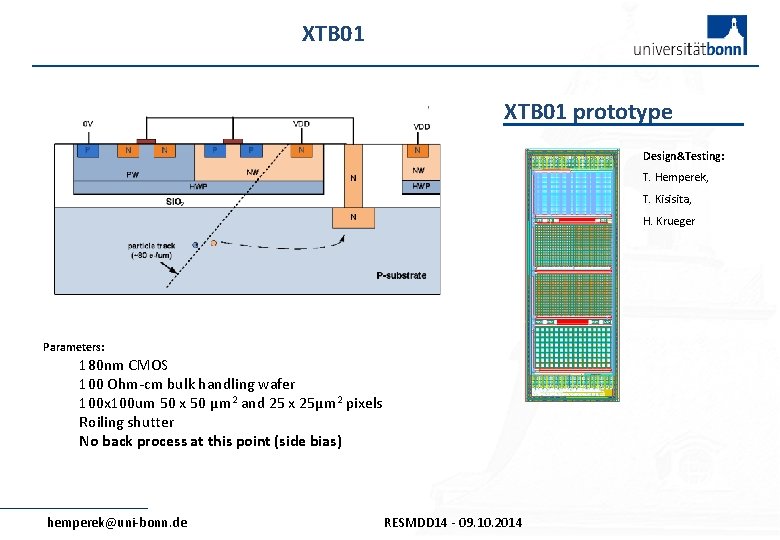
XTB 01 prototype Design&Testing: T. Hemperek, T. Kisisita, H. Krueger Parameters: 180 nm CMOS 100 Ohm-cm bulk handling wafer 100 x 100 um 50 x 50 µm 2 and 25 x 25µm 2 pixels Roiling shutter No back process at this point (side bias) hemperek@uni-bonn. de RESMDD 14 - 09. 10. 2014

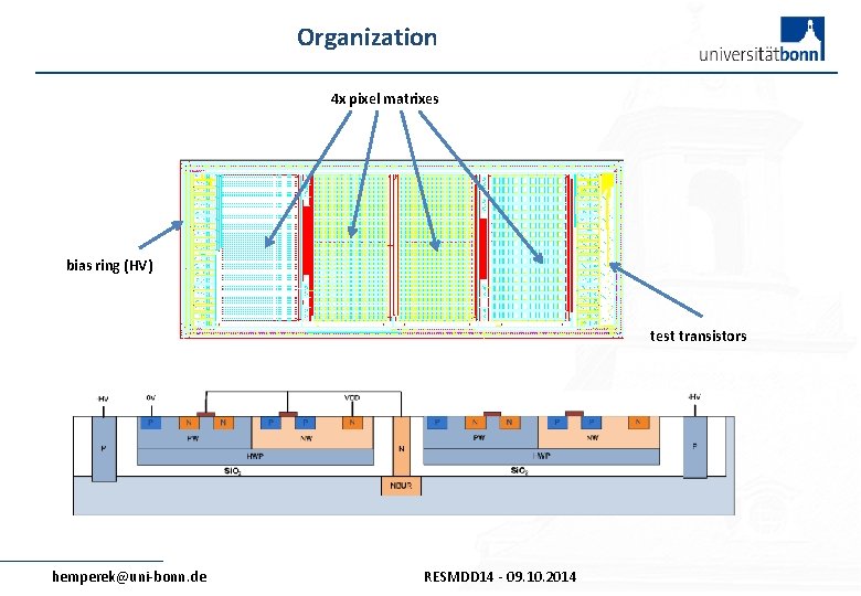
Organization 4 x pixel matrixes bias ring (HV) test transistors hemperek@uni-bonn. de RESMDD 14 - 09. 10. 2014

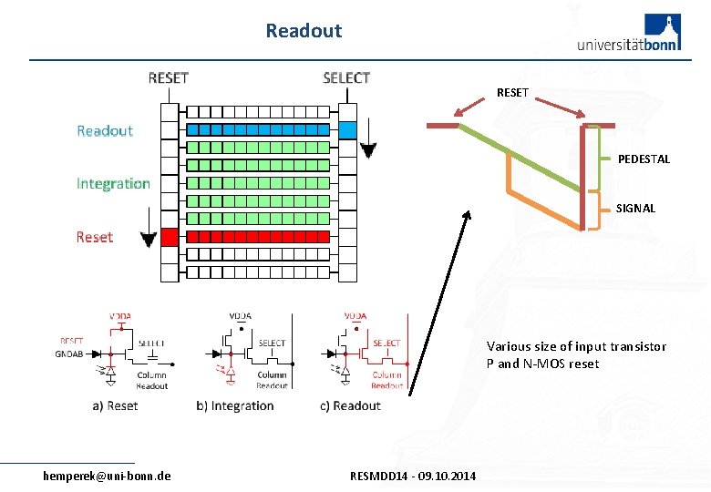
Readout RESET PEDESTAL SIGNAL Various size of input transistor P and N-MOS reset hemperek@uni-bonn. de RESMDD 14 - 09. 10. 2014

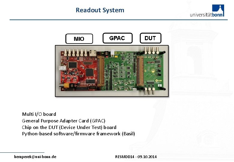
Readout System Multi I/O board General Purpose Adapter Card (GPAC) Chip on the DUT (Device Under Test) board Python-based software/firmware framework (Basil) hemperek@uni-bonn. de RESMDD 14 - 09. 10. 2014

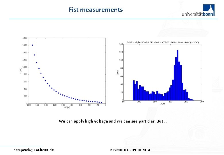
Fist measurements We can apply high voltage and we can see particles. But … hemperek@uni-bonn. de RESMDD 14 - 09. 10. 2014

Disclaimer I will concentrate on sensor performance. The transistors will be covered in the next talk. Presented measurements are conducted for first time on first prototypes on single samples. Have to be taken with some cautious. hemperek@uni-bonn. de RESMDD 14 - 09. 10. 2014

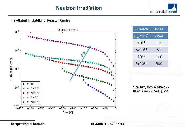
Neutron irradiation do se Irradiated in Ljubljana Reactor Centre Fluence Dose neq/cm 2 k. Rad 1013 10 5 x 10¹³ 50 1014 100 5 x 10¹⁴ 500 At 5 x 10¹⁴/300 V is 345 u. A -> 100 x 100 um -> 35 n. A @25 C hemperek@uni-bonn. de RESMDD 14 - 09. 10. 2014
![Depletion Width µm Depletion Width in Silicon 150 1000 Ohmcm 100 Ohmcm 50 0 Depletion Width [µm] Depletion Width in Silicon 150 1000 Ohm-cm 100 Ohm-cm 50 0](https://slidetodoc.com/presentation_image/1e08135608e12a733ac1c85b63f340d3/image-16.jpg)
Depletion Width [µm] Depletion Width in Silicon 150 1000 Ohm-cm 100 Ohm-cm 50 0 0 hemperek@uni-bonn. de 50 100 150 200 Reverse Bias Voltage [V] RESMDD 14 - 09. 10. 2014 250 300

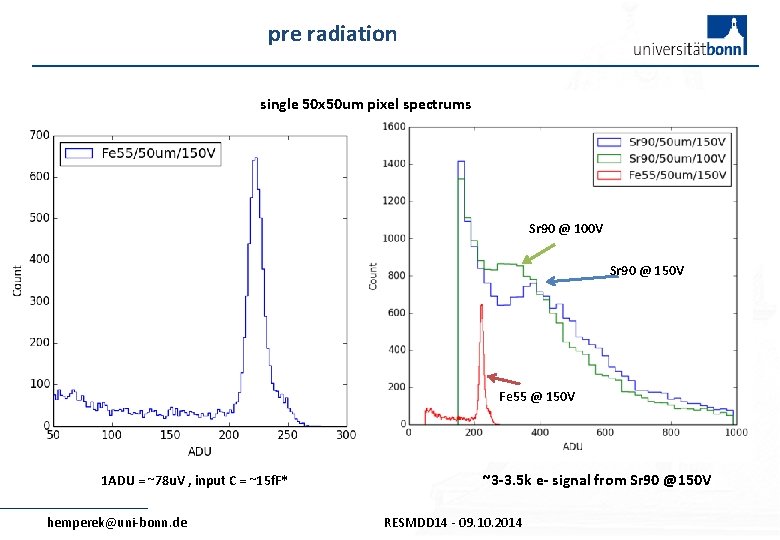
pre radiation single 50 x 50 um pixel spectrums Sr 90 @ 100 V Sr 90 @ 150 V Fe 55 @ 150 V 1 ADU = ~78 u. V , input C = ~15 f. F* hemperek@uni-bonn. de ~3 -3. 5 k e- signal from Sr 90 @150 V RESMDD 14 - 09. 10. 2014

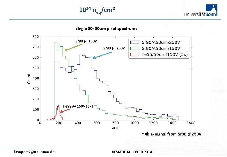
1014 neq/cm 2 single 50 x 50 um pixel spectrums Sr 90 @ 150 V Sr 90 @ 250 V Fe 55 @ 150 V (5 x) ~4 k e- signal from Sr 90 @250 V hemperek@uni-bonn. de RESMDD 14 - 09. 10. 2014

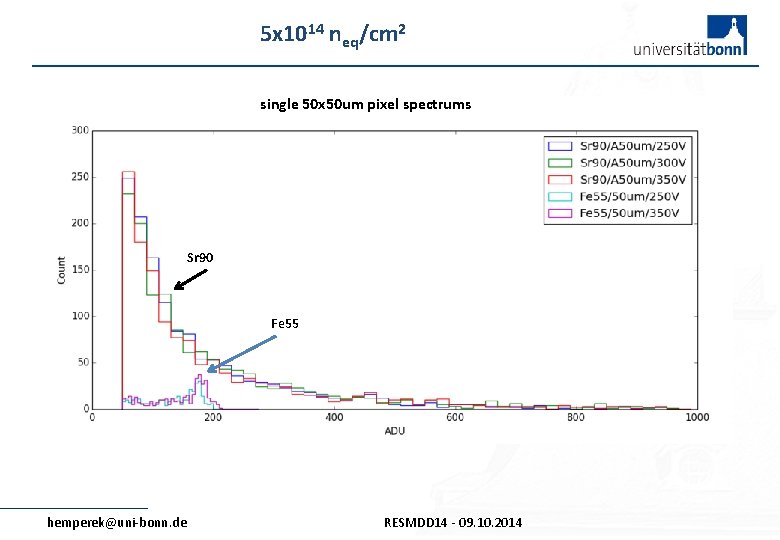
5 x 10¹⁴ neq/cm 2 single 50 x 50 um pixel spectrums Sr 90 Fe 55 hemperek@uni-bonn. de RESMDD 14 - 09. 10. 2014

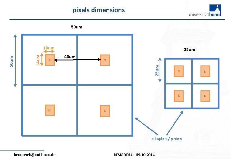
pixels dimensions 50 um N 25 um 40 um N 25 um 14 um 50 um 10 um N N N p implant/ p-stop hemperek@uni-bonn. de RESMDD 14 - 09. 10. 2014

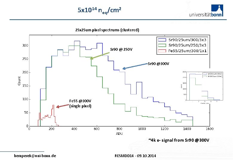
5 x 10¹⁴ neq/cm 2 25 x 25 um pixel spectrums (clustered) Sr 90 @ 250 V Sr 90 @300 V Fe 55 @300 V (single pixel) ~4 k e- signal from Sr 90 @300 V hemperek@uni-bonn. de RESMDD 14 - 09. 10. 2014

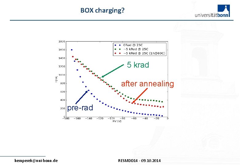
BOX charging? 5 krad after annealing pre-rad hemperek@uni-bonn. de RESMDD 14 - 09. 10. 2014

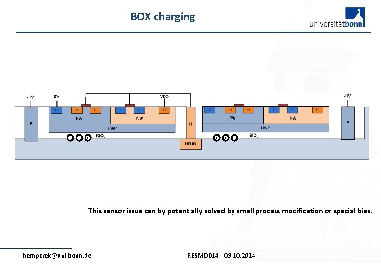
BOX charging + + + This sensor issue can by potentially solved by small process modification or special bias. hemperek@uni-bonn. de RESMDD 14 - 09. 10. 2014

Transistors Influence of BOX charging on transistors? hemperek@uni-bonn. de RESMDD 14 - 09. 10. 2014

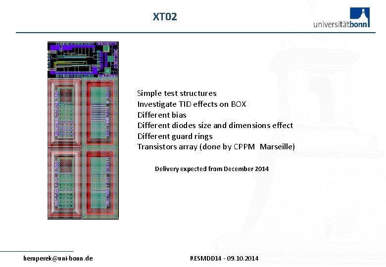
XT 02 Simple test structures Investigate TID effects on BOX Different bias Different diodes size and dimensions effect Different guard rings Transistors array (done by CPPM Marseille) Delivery expected from December 2014 hemperek@uni-bonn. de RESMDD 14 - 09. 10. 2014

Conclusion • First prototype in PD-SOI technology to be used for particle detections • No observed influence of oxide charges in the BOX on transistors • Indicate some negative influence of oxide charges bellow BOX on sensor (can be addressed by simple process/bias changes) • First measurements indicate signal of few thousands electrons signal even after 5 x 10¹⁴ neq/cm 2 (depends on diode configuration, more investigation and statistics needed) • Gives possibility to make pixelated fully monolithic (in pixel CMOS) radiation hard sensor • Large size design (full wafer) planed for 2015 also on 1 k Ohm-cm with possibility of thinning and back implantation. Implement proper readout (consider leakage) and measured capacitances. hemperek@uni-bonn. de RESMDD 14 - 09. 10. 2014

Backup hemperek@uni-bonn. de RESMDD 14 - 09. 10. 2014

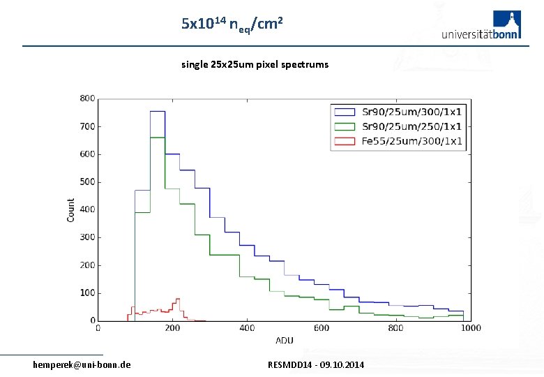
5 x 10¹⁴ neq/cm 2 single 25 x 25 um pixel spectrums hemperek@uni-bonn. de RESMDD 14 - 09. 10. 2014

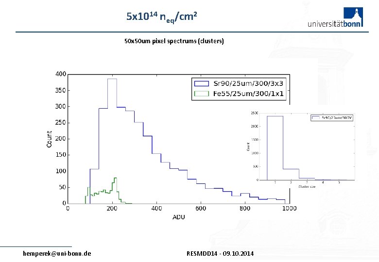
5 x 10¹⁴ neq/cm 2 50 x 50 um pixel spectrums (clusters) hemperek@uni-bonn. de RESMDD 14 - 09. 10. 2014

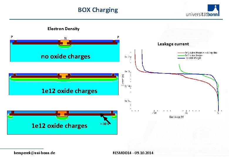
BOX Charging Electron Density P P N Leakage current no oxide charges 1 e 12 oxide charges hemperek@uni-bonn. de >-50 V RESMDD 14 - 09. 10. 2014

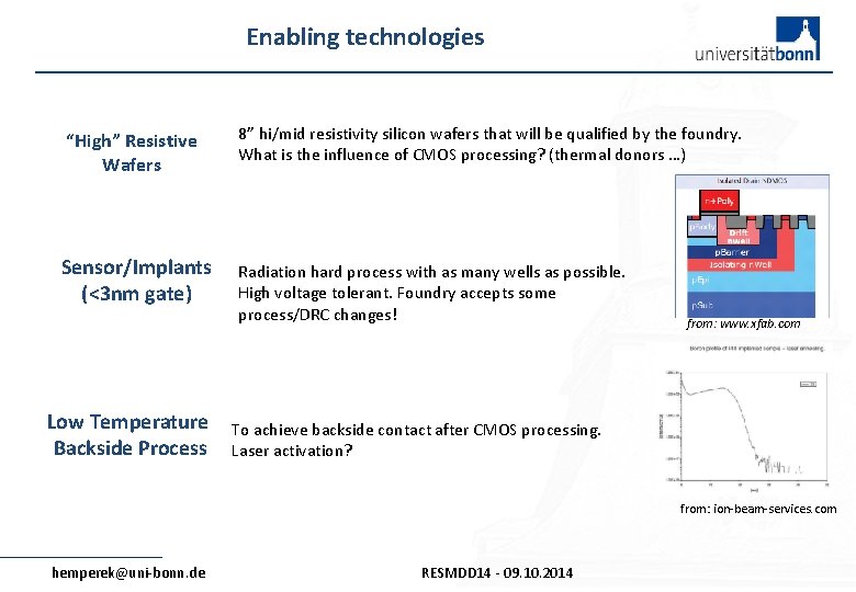
Enabling technologies “High” Resistive Wafers 8” hi/mid resistivity silicon wafers that will be qualified by the foundry. What is the influence of CMOS processing? (thermal donors …) Sensor/Implants (<3 nm gate) Radiation hard process with as many wells as possible. High voltage tolerant. Foundry accepts some process/DRC changes! Low Temperature Backside Process from: www. xfab. com To achieve backside contact after CMOS processing. Laser activation? from: ion-beam-services. com hemperek@uni-bonn. de RESMDD 14 - 09. 10. 2014

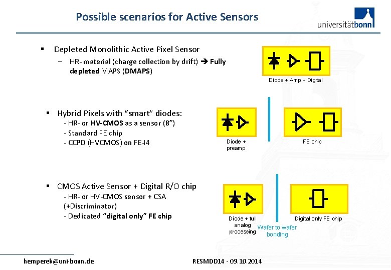
Possible scenarios for Active Sensors § Depleted Monolithic Active Pixel Sensor – HR- material (charge collection by drift) Fully depleted MAPS (DMAPS) Diode + Amp + Digital § Hybrid Pixels with “smart” diodes: - HR- or HV-CMOS as a sensor (8”) - Standard FE chip - CCPD (HVCMOS) on FE-I 4 FE chip Diode + preamp § CMOS Active Sensor + Digital R/O chip - HR- or HV-CMOS sensor + CSA (+Discriminator) - Dedicated “digital only” FE chip Diode + full Digital only FE chip analog Wafer to wafer processing bonding hemperek@uni-bonn. de RESMDD 14 - 09. 10. 2014