Monolithic Active Pixel Sensor for a TeraPixel ECAL
- Slides: 20

Monolithic Active Pixel Sensor for a “Tera-Pixel” ECAL at the ILC J. P. Crooks Y. Mikami, O. Miller, V. Rajovic, N. K. Watson, J. A. Wilson University of Birmingham J. A. Ballin, P. D. Dauncey, A. -M. Magnan, M. Noy Imperial College London J. P. Crooks, B. Levin, M. Lynch, M. Stanitzki, K. D. Stefanov, R. Turchetta, M. Tyndel, E. G. Villani STFC-Rutherford Appleton Laboratory

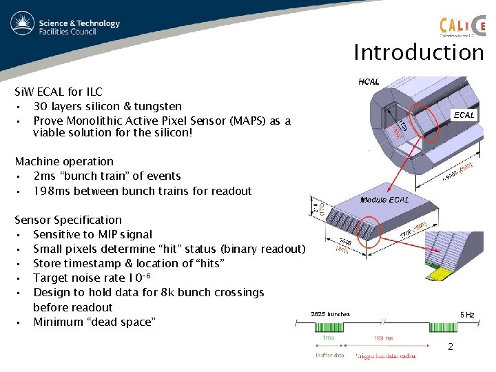
Introduction Si. W ECAL for ILC • 30 layers silicon & tungsten • Prove Monolithic Active Pixel Sensor (MAPS) as a viable solution for the silicon! Machine operation • 2 ms “bunch train” of events • 198 ms between bunch trains for readout Sensor Specification • Sensitive to MIP signal • Small pixels determine “hit” status (binary readout) • Store timestamp & location of “hits” • Target noise rate 10 -6 • Design to hold data for 8 k bunch crossings before readout • Minimum “dead space” 2625 bunches 2

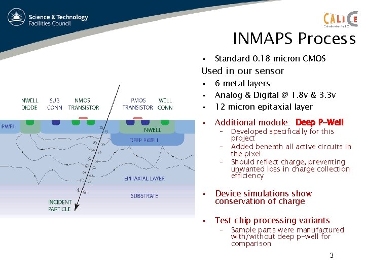
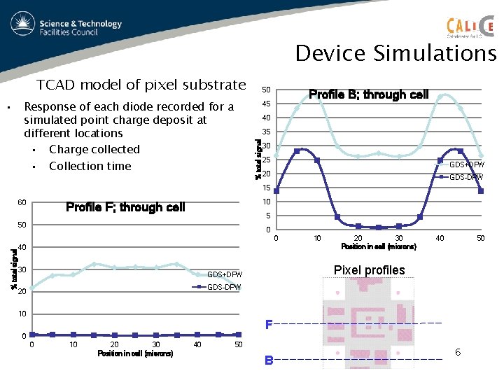
INMAPS Process • Standard 0. 18 micron CMOS • • • 6 metal layers Analog & Digital @ 1. 8 v & 3. 3 v 12 micron epitaxial layer • Additional module: Deep P-Well Used in our sensor – – – Developed specifically for this project Added beneath all active circuits in the pixel Should reflect charge, preventing unwanted loss in charge collection efficiency • Device simulations show conservation of charge • Test chip processing variants – Sample parts were manufactured with/without deep p-well for comparison 3

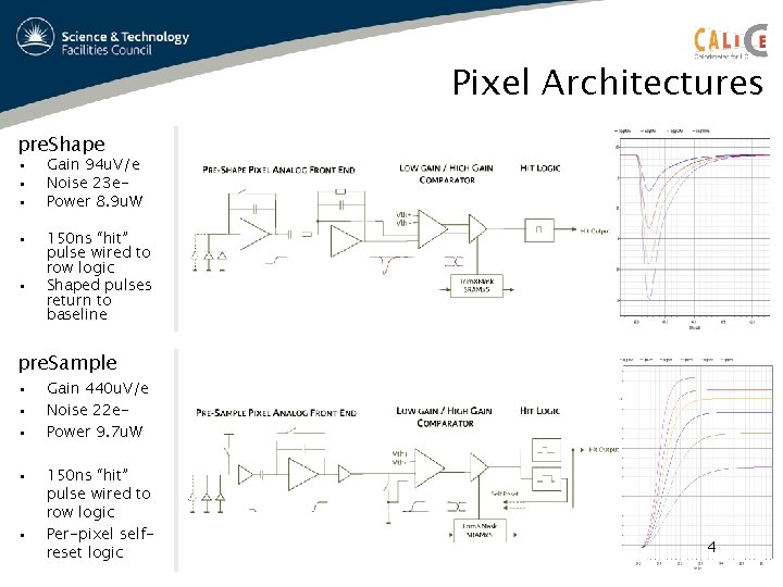
Pixel Architectures pre. Shape • • • Gain 94 u. V/e Noise 23 e. Power 8. 9 u. W • 150 ns “hit” pulse wired to row logic Shaped pulses return to baseline • pre. Sample • • • Gain 440 u. V/e Noise 22 e. Power 9. 7 u. W • 150 ns “hit” pulse wired to row logic Per-pixel selfreset logic • 4

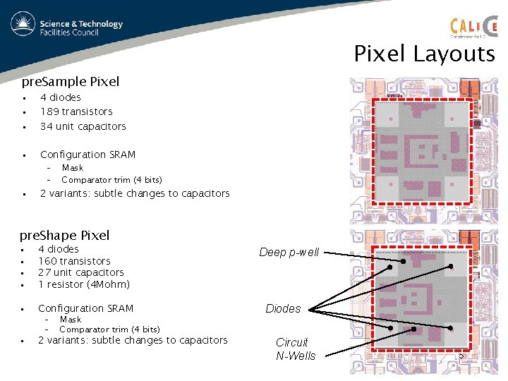
Pixel Layouts pre. Sample Pixel • • • 4 diodes 189 transistors 34 unit capacitors • Configuration SRAM • 2 variants: subtle changes to capacitors – – Mask Comparator trim (4 bits) pre. Shape Pixel • • 4 diodes 160 transistors 27 unit capacitors 1 resistor (4 Mohm) • Configuration SRAM • 2 variants: subtle changes to capacitors – – Mask Comparator trim (4 bits) Deep p-well Diodes Circuit N-Wells 5

Device Simulations TCAD model of pixel substrate Response of each diode recorded for a simulated point charge deposit at different locations • Charge collected • Collection time Profile B; through cell 45 40 35 % total signal • 50 30 25 GDS+DPW 20 GDS-DPW 15 60 10 Profile F; through cell 5 50 0 % total signal 0 40 30 10 20 30 Position in cell (microns) 40 50 Pixel profiles GDS+DPW GDS-DPW 20 10 F 0 0 10 20 30 Position in cell (microns) 40 50 B 6

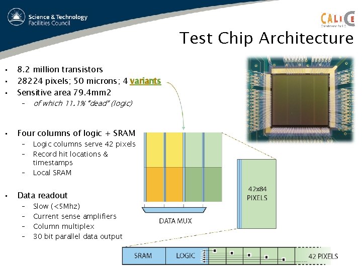
Test Chip Architecture • • • 8. 2 million transistors 28224 pixels; 50 microns; 4 variants Sensitive area 79. 4 mm 2 • Four columns of logic + SRAM – – • of which 11. 1% “dead” (logic) Logic columns serve 42 pixels Record hit locations & timestamps Local SRAM Data readout – – Slow (<5 Mhz) Current sense amplifiers Column multiplex 30 bit parallel data output

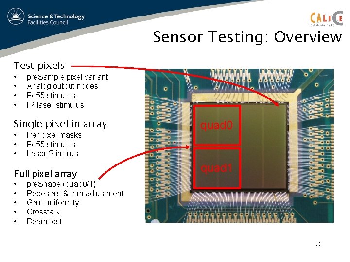
Sensor Testing: Overview Test pixels • • pre. Sample pixel variant Analog output nodes Fe 55 stimulus IR laser stimulus Single pixel in array • • • Per pixel masks Fe 55 stimulus Laser Stimulus Full pixel array • • • quad 0 quad 1 pre. Shape (quad 0/1) Pedestals & trim adjustment Gain uniformity Crosstalk Beam test 8

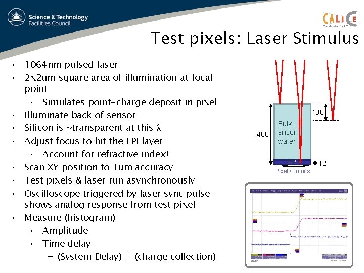
Test pixels: Laser Stimulus • 1064 nm pulsed laser • 2 x 2 um square area of illumination at focal point • Simulates point-charge deposit in pixel • Illuminate back of sensor • Silicon is ~transparent at this λ • Adjust focus to hit the EPI layer • Account for refractive index! • Scan XY position to 1 um accuracy • Test pixels & laser run asynchronously • Oscilloscope triggered by laser sync pulse shows analog response from test pixel • Measure (histogram) • Amplitude • Time delay = (System Delay) + (charge collection) 100 400 Bulk silicon wafer EPI Pixel Circuits 12

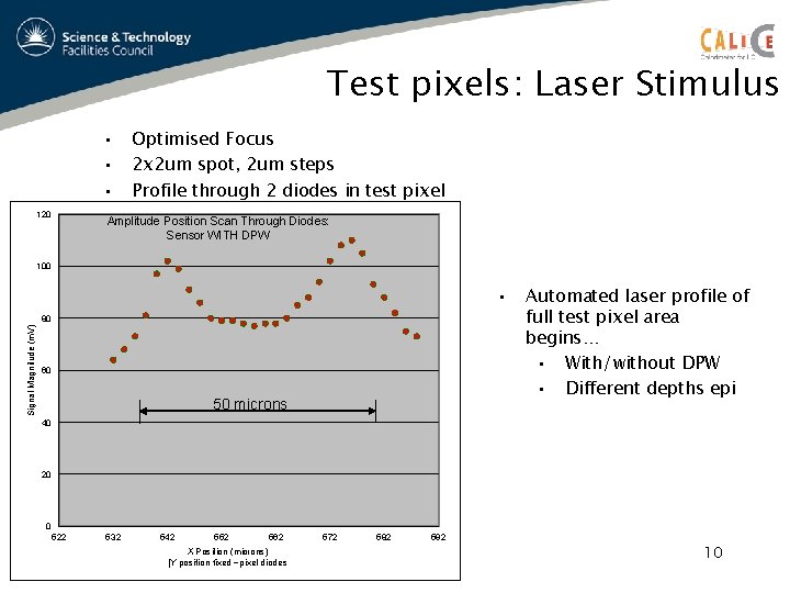
Test pixels: Laser Stimulus • • • 120 Optimised Focus 2 x 2 um spot, 2 um steps Profile through 2 diodes in test pixel Amplitude Position Scan Through Diodes: Sensor WITH DPW 100 • Signal Magnitude (m. V) 80 60 50 microns Automated laser profile of full test pixel area begins… • With/without DPW • Different depths epi 40 20 0 522 532 542 552 562 X Position (microns) [Y position fixed ~pixel diodes 572 582 592 10

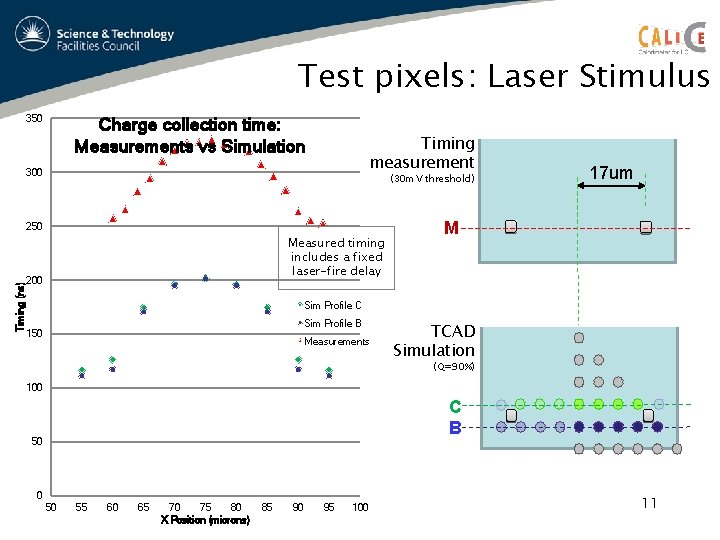
Test pixels: Laser Stimulus 350 Charge collection time: Measurements vs Simulation Timing measurement 300 (30 m. V threshold) Timing (ns) 250 Measured timing includes a fixed laser-fire delay 200 17 um M Sim Profile C Sim Profile B 150 Measurements TCAD Simulation (Q=90%) 100 C B 50 0 50 55 60 65 70 75 80 X Position (microns) 85 90 95 100 11

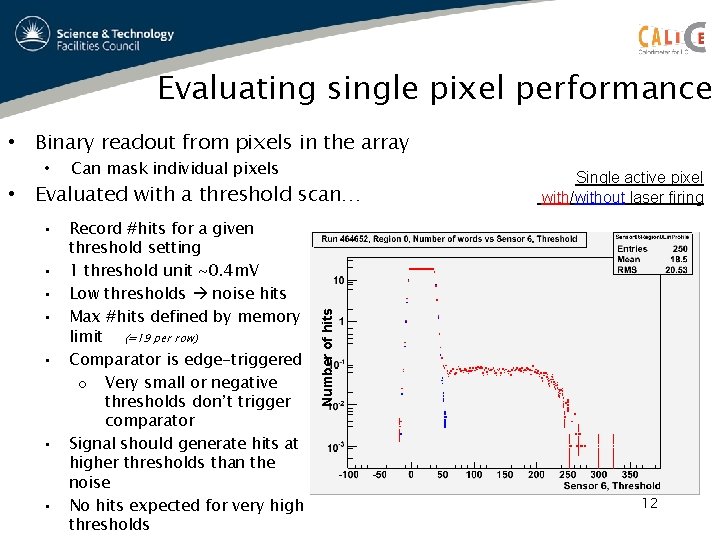
Evaluating single pixel performance • Binary readout from pixels in the array • Can mask individual pixels • • Record #hits for a given threshold setting 1 threshold unit ~0. 4 m. V Low thresholds noise hits Max #hits defined by memory limit (=19 per row) Comparator is edge-triggered o Very small or negative thresholds don’t trigger comparator Signal should generate hits at higher thresholds than the noise No hits expected for very high thresholds Number of hits • Evaluated with a threshold scan… Single active pixel with/without laser firing 12

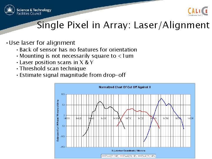
Single Pixel in Array: Laser/Alignment • Use laser for alignment • Back of sensor has no features for orientation • Mounting is not necessarily square to <1 um • Laser position scans in X & Y • Threshold scan technique • Estimate signal magnitude from drop-off 13

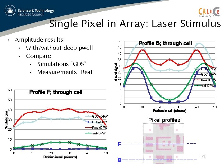
Single Pixel in Array: Laser Stimulus • Amplitude results • With/without deep pwell • Compare • Simulations “GDS” • Measurements “Real” 50 Profile B; through cell 45 40 % total signal 35 30 GDS+DPW 25 GDS-DPW 20 Real+DPW 15 60 Profile F; through cell 10 5 50 % total signal real-DPW 0 0 40 GDS+DPW 30 10 20 30 Position in cell (microns) 40 50 Pixel profiles GDS-DPW Real+DPW 20 real-DPW 10 F 0 0 10 20 30 Position in cell (microns) 40 50 B 14

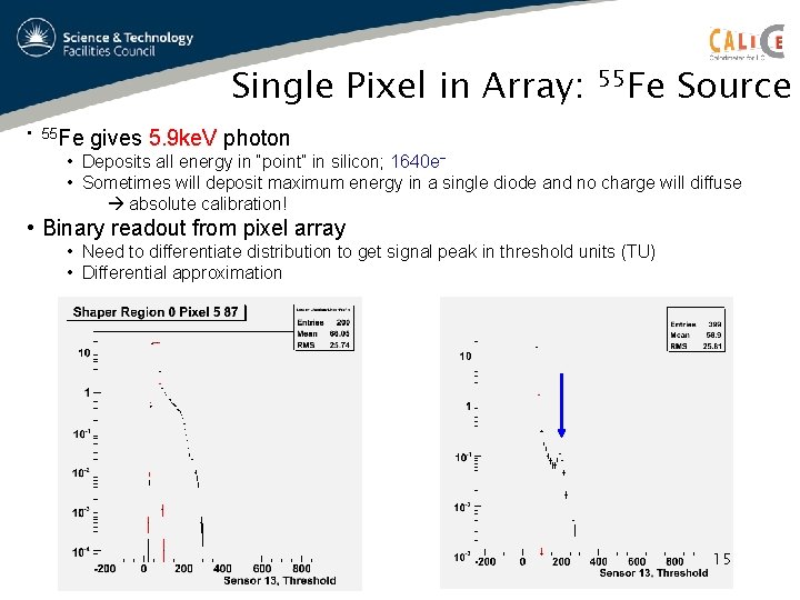
Single Pixel in Array: • 55 Fe Source gives 5. 9 ke. V photon • Deposits all energy in “point” in silicon; 1640 e− • Sometimes will deposit maximum energy in a single diode and no charge will diffuse absolute calibration! • Binary readout from pixel array • Need to differentiate distribution to get signal peak in threshold units (TU) • Differential approximation 15

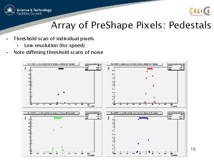
Array of Pre. Shape Pixels: Pedestals • • Threshold scan of individual pixels • Low resolution (for speed) Note differing threshold scans of noise 16

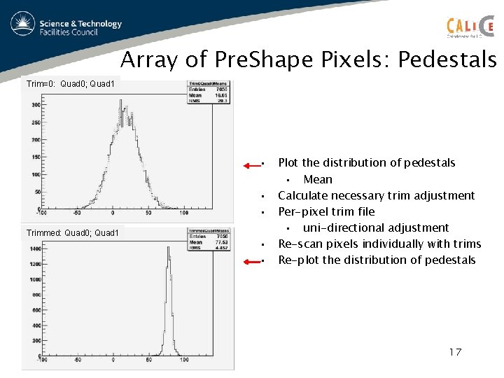
Array of Pre. Shape Pixels: Pedestals Trim=0: Quad 0; Quad 1 • • • Trimmed: Quad 0; Quad 1 • • Plot the distribution of pedestals • Mean Calculate necessary trim adjustment Per-pixel trim file • uni-directional adjustment Re-scan pixels individually with trims Re-plot the distribution of pedestals 17

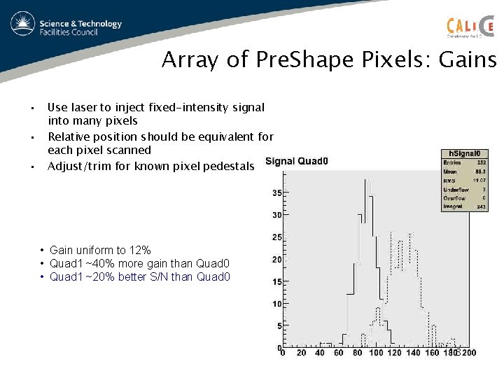
Array of Pre. Shape Pixels: Gains • • • Use laser to inject fixed-intensity signal into many pixels Relative position should be equivalent for each pixel scanned Adjust/trim for known pixel pedestals • Gain uniform to 12% • Quad 1 ~40% more gain than Quad 0 • Quad 1 ~20% better S/N than Quad 0 18

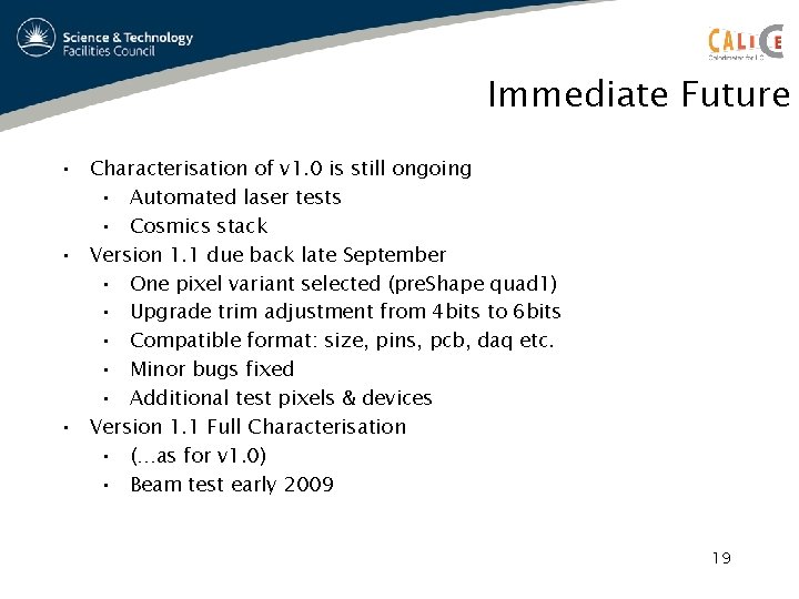
Immediate Future • Characterisation of v 1. 0 is still ongoing • Automated laser tests • Cosmics stack • Version 1. 1 due back late September • One pixel variant selected (pre. Shape quad 1) • Upgrade trim adjustment from 4 bits to 6 bits • Compatible format: size, pins, pcb, daq etc. • Minor bugs fixed • Additional test pixels & devices • Version 1. 1 Full Characterisation • (…as for v 1. 0) • Beam test early 2009 19

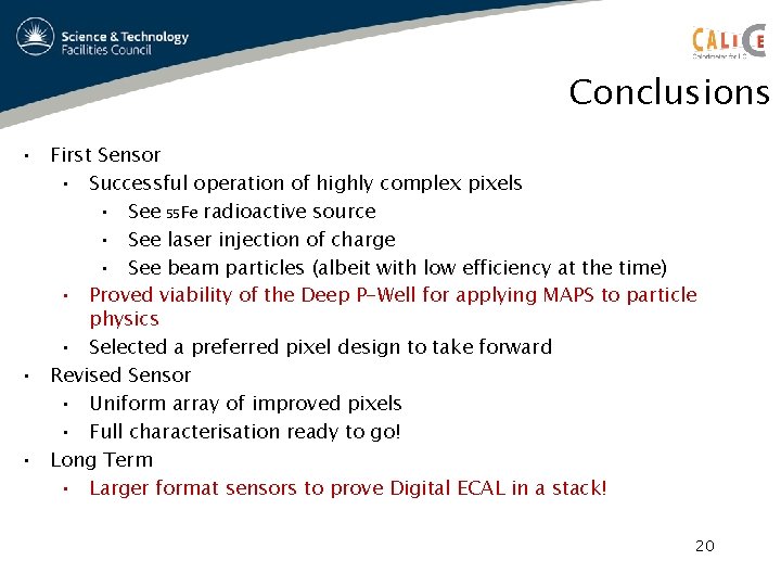
Conclusions • First Sensor • Successful operation of highly complex pixels • See 55 Fe radioactive source • See laser injection of charge • See beam particles (albeit with low efficiency at the time) • Proved viability of the Deep P-Well for applying MAPS to particle physics • Selected a preferred pixel design to take forward • Revised Sensor • Uniform array of improved pixels • Full characterisation ready to go! • Long Term • Larger format sensors to prove Digital ECAL in a stack! 20