Monolithic Active Pixel Sensor Development for the Upgrade

![Priority Encoder readout v[0] valid v[1] v[2] select v[3] sel[0] sel[1] sel[2] a[0] sel[3] Priority Encoder readout v[0] valid v[1] v[2] select v[3] sel[0] sel[1] sel[2] a[0] sel[3]](https://slidetodoc.com/presentation_image_h2/e05375c298f92cc3b245aee30f5a35fb/image-22.jpg)
- Slides: 28

Monolithic Active Pixel Sensor Development for the Upgrade of the ALICE Inner Tracker System CERN/INFN/WUHAN ALICE ITS team C. Cavicchioli, P. L. Chalmet, P. Giubilato, H. Hillemanns, A. Junique, T. Kugathasan, A. Lattuca, M. Mager, C. A. Marin Tobon, P. Martinengo, S. Mattiazzo, G. Mazza, H. Mugnier, L. Musa, D. Pantano, J. Rousset, F. Reidt, P. Riedler, W. Snoeys, J. W. van Hoorne, P. Yang

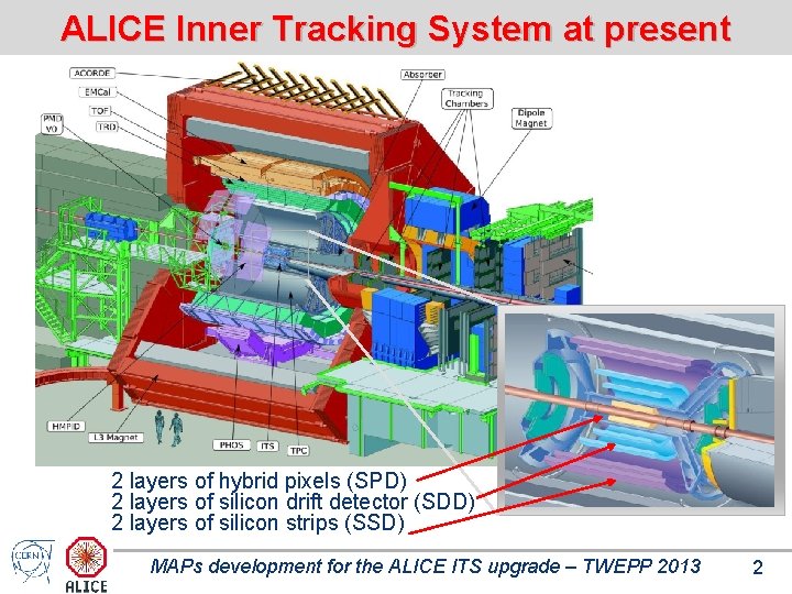
ALICE Inner Tracking System at present 2 layers of hybrid pixels (SPD) 2 layers of silicon drift detector (SDD) 2 layers of silicon strips (SSD) MAPs development for the ALICE ITS upgrade – TWEPP 2013 2

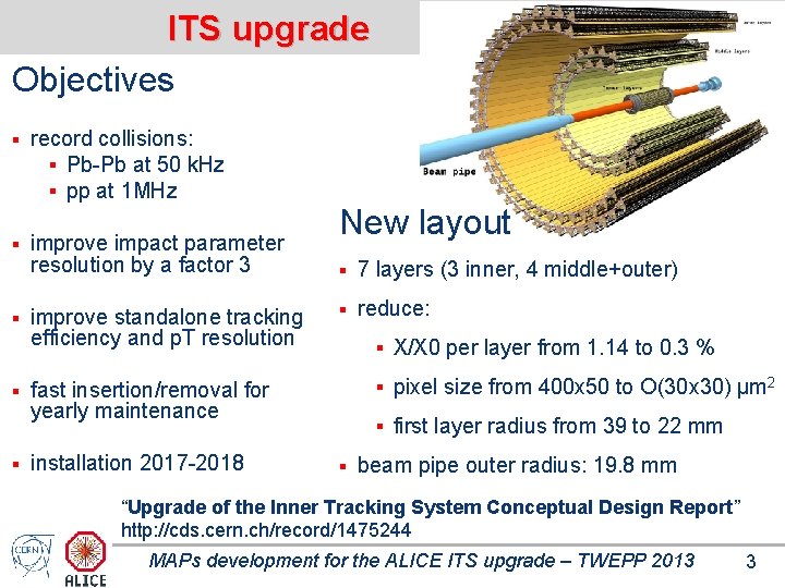
ITS upgrade Objectives § § § record collisions: § Pb-Pb at 50 k. Hz § pp at 1 MHz improve impact parameter resolution by a factor 3 improve standalone tracking efficiency and p. T resolution New layout § 7 layers (3 inner, 4 middle+outer) § reduce: § X/X 0 per layer from 1. 14 to 0. 3 % § pixel size from 400 x 50 to O(30 x 30) μm 2 fast insertion/removal for yearly maintenance installation 2017 -2018 § first layer radius from 39 to 22 mm § beam pipe outer radius: 19. 8 mm “Upgrade of the Inner Tracking System Conceptual Design Report” http: //cds. cern. ch/record/1475244 MAPs development for the ALICE ITS upgrade – TWEPP 2013 3

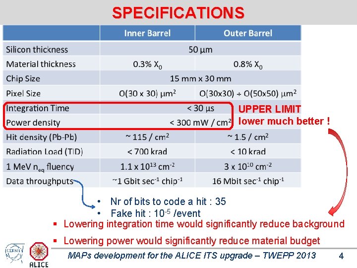
SPECIFICATIONS UPPER LIMIT lower much better ! • Nr of bits to code a hit : 35 • Fake hit : 10 -5 /event § Lowering integration time would significantly reduce background § Lowering power would significantly reduce material budget MAPs development for the ALICE ITS upgrade – TWEPP 2013 4

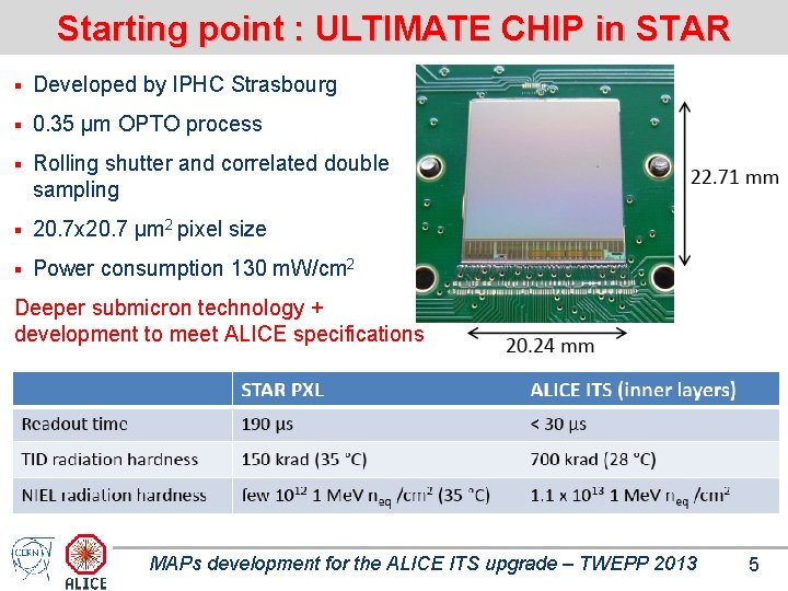
Starting point : ULTIMATE CHIP in STAR § Developed by IPHC Strasbourg § 0. 35 μm OPTO process § Rolling shutter and correlated double sampling § 20. 7 x 20. 7 μm 2 pixel size § Power consumption 130 m. W/cm 2 Deeper submicron technology + development to meet ALICE specifications MAPs development for the ALICE ITS upgrade – TWEPP 2013 5

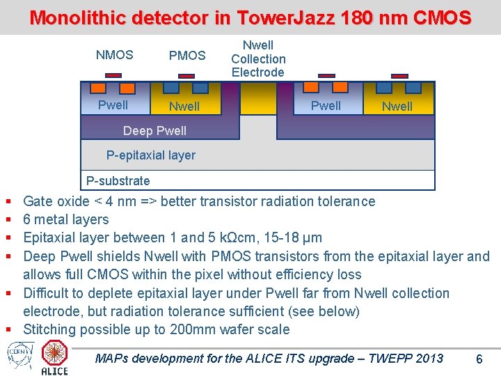
Monolithic detector in Tower. Jazz 180 nm CMOS NMOS Pwell Nwell Collection Electrode Pwell Nwell Deep Pwell P-epitaxial layer P-substrate § § Gate oxide < 4 nm => better transistor radiation tolerance 6 metal layers Epitaxial layer between 1 and 5 kΩcm, 15 -18 μm Deep Pwell shields Nwell with PMOS transistors from the epitaxial layer and allows full CMOS within the pixel without efficiency loss § Difficult to deplete epitaxial layer under Pwell far from Nwell collection electrode, but radiation tolerance sufficient (see below) § Stitching possible up to 200 mm wafer scale MAPs development for the ALICE ITS upgrade – TWEPP 2013 6

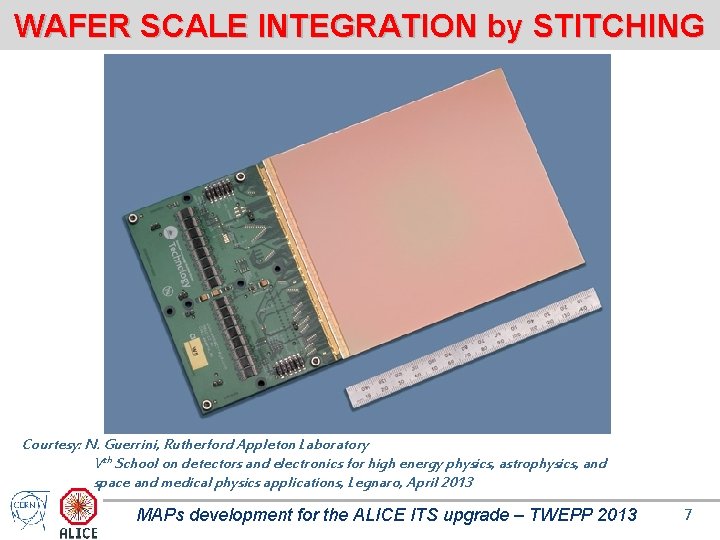
WAFER SCALE INTEGRATION by STITCHING Courtesy: N. Guerrini, Rutherford Appleton Laboratory Vth School on detectors and electronics for high energy physics, astrophysics, and space and medical physics applications, Legnaro, April 2013 MAPs development for the ALICE ITS upgrade – TWEPP 2013 7

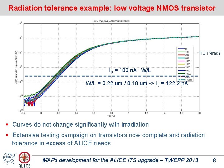
Radiation tolerance example: low voltage NMOS transistor TID (Mrad) I 0 = 100 n. A. W/L = 0. 22 um / 0. 18 um -> I 0 = 122. 2 n. A § Curves do not change significantly with irradiation § Extensive testing campaign on transistors now complete and radiation tolerance in excess of ALICE needs MAPs development for the ALICE ITS upgrade – TWEPP 2013 8

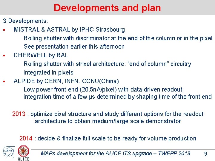
Developments and plan 3 Developments: § MISTRAL & ASTRAL by IPHC Strasbourg Rolling shutter with discriminator at the end of the column or in the pixel See presentation earlier this afternoon § CHERWELL by RAL Rolling shutter with strixel architecture: “end of column” circuitry integrated in pixels § ALPIDE by CERN, INFN, CCNU(China) Low power front-end (20. 5 n. A/pixel) with data-driven readout, integration time of a few μs determined by shaping time of the front end 2013 : optimize pixel structure and study different options for the readout architecture to obtain medium/large scale demonstrator 2014 : decide & finalize full scale to be ready for volume production MAPs development for the ALICE ITS upgrade – TWEPP 2013 9

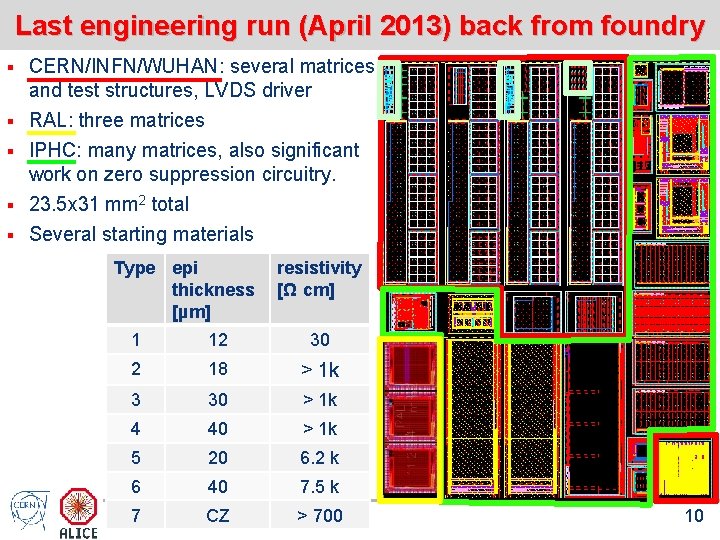
Last engineering run (April 2013) back from foundry § CERN/INFN/WUHAN: several matrices and test structures, LVDS driver § RAL: three matrices IPHC: many matrices, also significant work on zero suppression circuitry. 23. 5 x 31 mm 2 total Several starting materials § § § Type epi thickness [µm] resistivity [Ω cm] 1 12 30 2 18 > 1 k 3 30 > 1 k 4 40 > 1 k 5 20 6. 2 k 6 40 7. 5 k 7 CZ > 700 10

EXPLORER : PIXEL SENSOR OPTIMIZATION and MEASUREMENTS

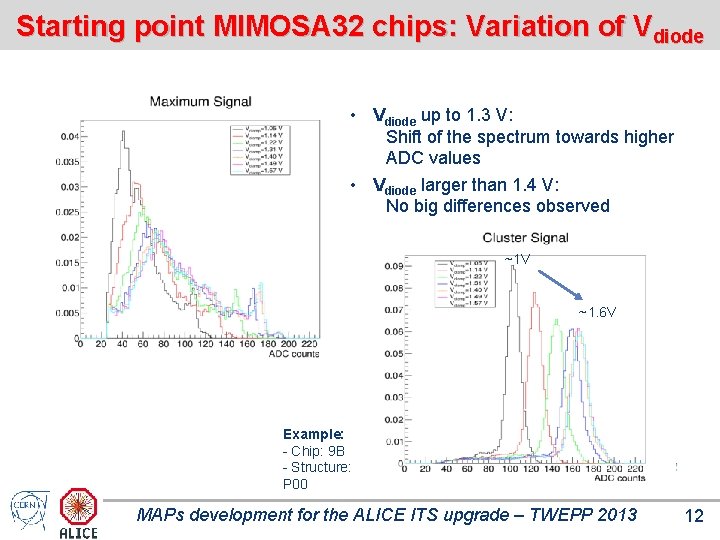
Starting point MIMOSA 32 chips: Variation of Vdiode • Vdiode up to 1. 3 V: Shift of the spectrum towards higher ADC values • Vdiode larger than 1. 4 V: No big differences observed ~1 V ~1. 6 V Example: - Chip: 9 B - Structure: P 00 MAPs development for the ALICE ITS upgrade – TWEPP 2013 12

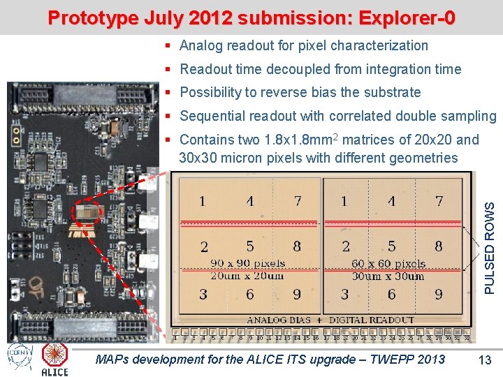
Prototype July 2012 submission: Explorer-0 § Analog readout for pixel characterization § Readout time decoupled from integration time § Possibility to reverse bias the substrate § Sequential readout with correlated double sampling PULSED ROWS § Contains two 1. 8 x 1. 8 mm 2 matrices of 20 x 20 and 30 x 30 micron pixels with different geometries MAPs development for the ALICE ITS upgrade – TWEPP 2013 13

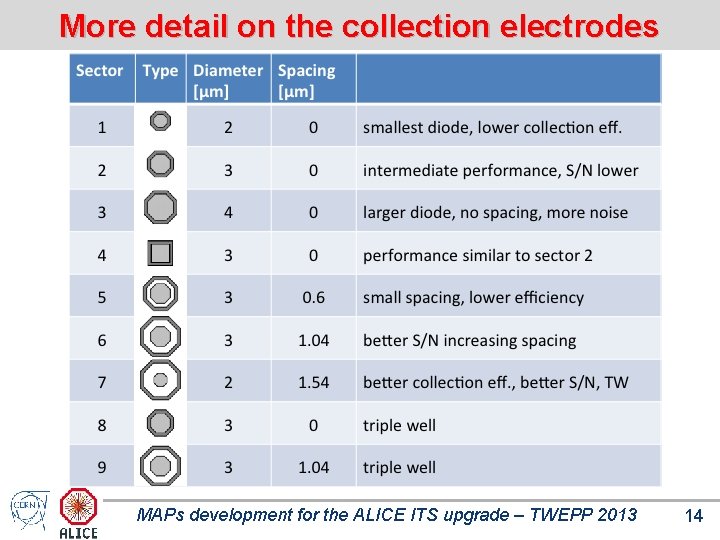
More detail on the collection electrodes MAPs development for the ALICE ITS upgrade – TWEPP 2013 14

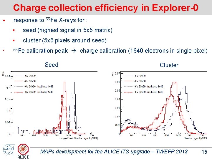
Charge collection efficiency in Explorer-0 § § response to 55 Fe X-rays for : § seed (highest signal in 5 x 5 matrix) § cluster (5 x 5 pixels around seed) 55 Fe calibration peak charge calibration (1640 electrons in single pixel) Seed Cluster MAPs development for the ALICE ITS upgrade – TWEPP 2013 15

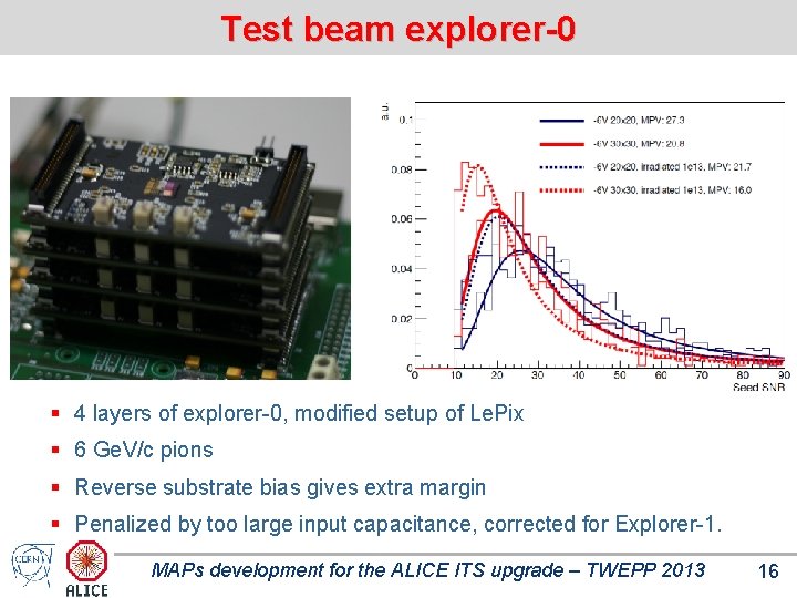
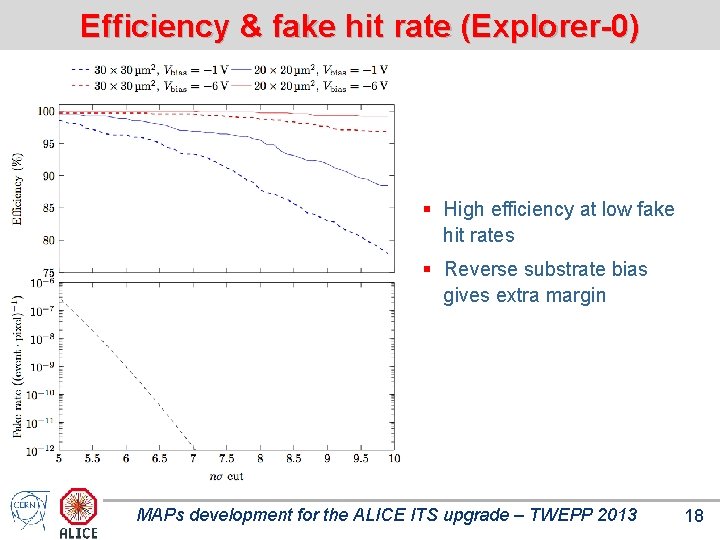
Test beam explorer-0 § 4 layers of explorer-0, modified setup of Le. Pix § 6 Ge. V/c pions § Reverse substrate bias gives extra margin § Penalized by too large input capacitance, corrected for Explorer-1. MAPs development for the ALICE ITS upgrade – TWEPP 2013 16

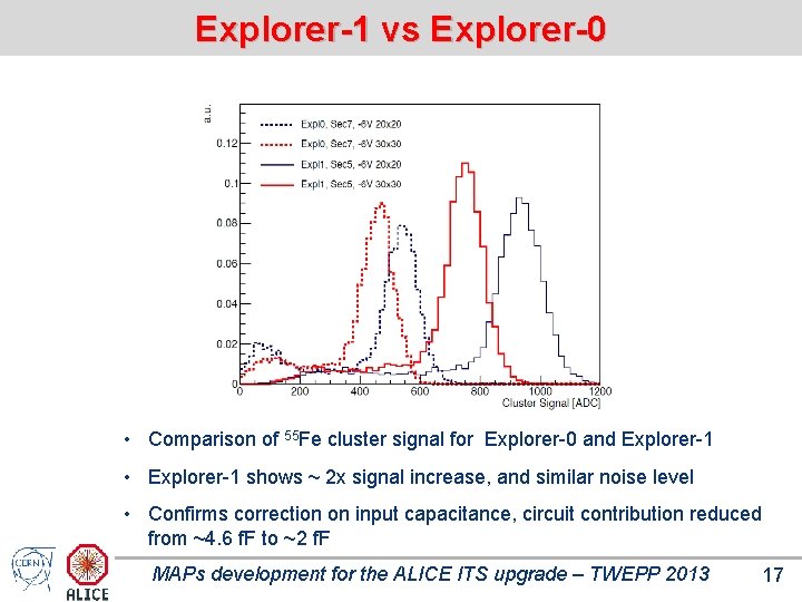
Explorer-1 vs Explorer-0 • Comparison of 55 Fe cluster signal for Explorer-0 and Explorer-1 • Explorer-1 shows ~ 2 x signal increase, and similar noise level • Confirms correction on input capacitance, circuit contribution reduced from ~4. 6 f. F to ~2 f. F MAPs development for the ALICE ITS upgrade – TWEPP 2013 17

Efficiency & fake hit rate (Explorer-0) § High efficiency at low fake hit rates § Reverse substrate bias gives extra margin MAPs development for the ALICE ITS upgrade – TWEPP 2013 18

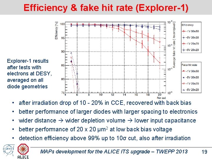
Efficiency & fake hit rate (Explorer-1) Explorer-1 results after tests with electrons at DESY, averaged on all diode geometries • • • after irradiation drop of 10 - 20% in CCE, recovered with back bias better performance of larger diodes with larger spacing to electronics wider distance wider depletion volume lower input capacitance better performance of 20 x 20 µm 2 at low back bias voltage detection efficiency above 99% up to 10σ cut, also after irradiation MAPs development for the ALICE ITS upgrade – TWEPP 2013 19

(p)ALPIDE FRONT END AND READOUT

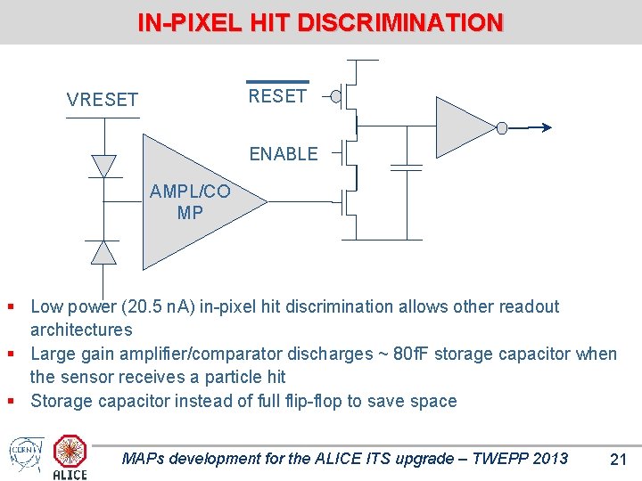
IN-PIXEL HIT DISCRIMINATION RESET VRESET ENABLE AMPL/CO MP § Low power (20. 5 n. A) in-pixel hit discrimination allows other readout architectures § Large gain amplifier/comparator discharges ~ 80 f. F storage capacitor when the sensor receives a particle hit § Storage capacitor instead of full flip-flop to save space MAPs development for the ALICE ITS upgrade – TWEPP 2013 21
![Priority Encoder readout v0 valid v1 v2 select v3 sel0 sel1 sel2 a0 sel3 Priority Encoder readout v[0] valid v[1] v[2] select v[3] sel[0] sel[1] sel[2] a[0] sel[3]](https://slidetodoc.com/presentation_image_h2/e05375c298f92cc3b245aee30f5a35fb/image-22.jpg)
Priority Encoder readout v[0] valid v[1] v[2] select v[3] sel[0] sel[1] sel[2] a[0] sel[3] a[1] § hierarchical readout § 4 inputs basic block repeated to create a larger encoder § 1 pixel read per clock cycle § forward path (address encoder) in gray § feed-back path (pixel reset) in red § asynchronous (combinatorial) logic § clock only to periphery, synchronous select only to hit pixels PIXEL COLUMN v[0] valid v[1] v[2] select v[3] sel[0] sel[1] sel[2] a[0] sel[3] a[1] VALID Periphery SELECT logic CLOCK TRIGGER v[0] valid v[1] v[2] select v[3] sel[0] sel[1] sel[2] a[0] sel[3] a[1] ADDR[0: 1] ADDR[2: 3] MAPs development for the ALICE ITS upgrade – TWEPP 2013 22

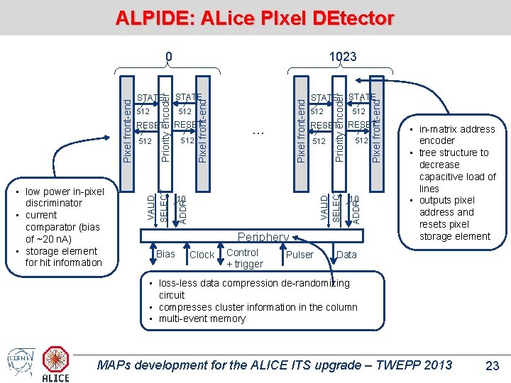
ALPIDE: ALice PIxel DEtector 512 10 512 RESET 512 10 Periphery Bias Clock Control + trigger Pulser Pixel front-end RESET STATE ADDR 512 Priority encoder 512 … STATE VALID SELECT 512 RESET Pixel front-end RESET 512 Pixel front-end Priority encoder 512 STATE ADDR • low power in-pixel discriminator • current comparator (bias of ~20 n. A) • storage element for hit information STATE 1023 VALID SELECT Pixel front-end 0 • in-matrix address encoder • tree structure to decrease capacitive load of lines • outputs pixel address and resets pixel storage element Data • loss-less data compression de-randomizing circuit • compresses cluster information in the column • multi-event memory MAPs development for the ALICE ITS upgrade – TWEPP 2013 23

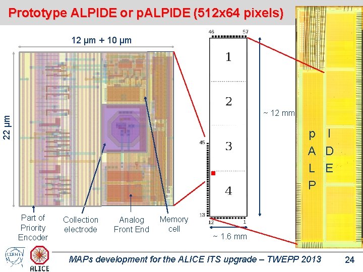
Prototype ALPIDE or p. ALPIDE (512 x 64 pixels) 12 µm + 10 µm 22 µm ~ 12 mm p I A D L E P Part of Priority Encoder Collection electrode Analog Front End Memory cell ~ 1. 6 mm MAPs development for the ALICE ITS upgrade – TWEPP 2013 24

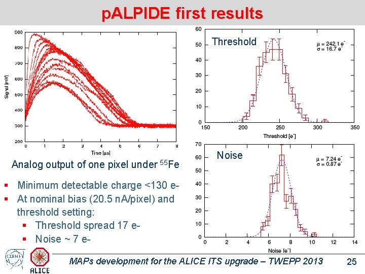
p. ALPIDE first results Threshold Analog output of one pixel under 55 Fe Noise § Minimum detectable charge <130 e§ At nominal bias (20. 5 n. A/pixel) and threshold setting: § Threshold spread 17 e§ Noise ~ 7 e. MAPs development for the ALICE ITS upgrade – TWEPP 2013 25

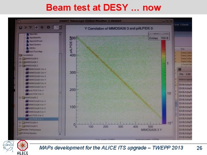
Beam test at DESY … now MAPs development for the ALICE ITS upgrade – TWEPP 2013 26

CONCLUSIONS § Pixel sensor § 100 m. V distributed over a few pixels § Could we get to digital signal by further optimization? § Analog front end design: 40 n. W*250 000 pixels = 10 m. W/cm 2 Promising results, but more work and checking needed. § Digital: looking at solution around 10 m. W/cm 2 § Off-chip data transmission ~ 30 -50 m. W/chip or <10 m. W/cm 2 Trying to approach strip level power consumption per unit area and stay below 50 m. W/cm 2 § Radiation tolerance sufficient for Alice § Significant work in progress in design and in test MAPs development for the ALICE ITS upgrade – TWEPP 2013 27

THANK YOU ! MAPs development for the ALICE ITS upgrade – TWEPP 2013 28