
Monolithic 3 DICs with Single Crystal Silicon Layers

- Slides: 46
Monolithic 3 D-ICs with Single Crystal Silicon Layers Deepak C. Sekar and Zvi Or-Bach Monolith. IC 3 D Inc. Monolith. IC Inc. Patents. Integration Pending 2012 IEEE 3 D 3 D System 1
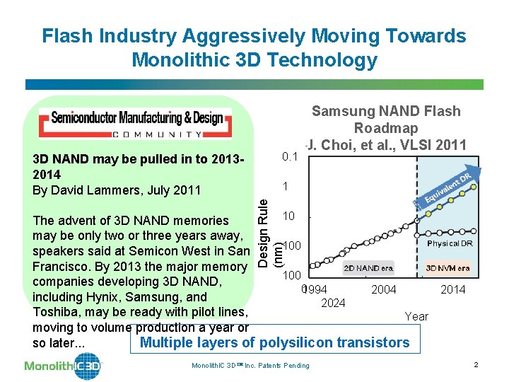
Flash Industry Aggressively Moving Towards Monolithic 3 D Technology 0. 1 1 Design Rule (nm) 3 D NAND may be pulled in to 20132014 By David Lammers, July 2011 Samsung NAND Flash Roadmap J. Choi, et al. , VLSI 2011 10 The advent of 3 D NAND memories may be only two or three years away, 100 speakers said at Semicon West in San Francisco. By 2013 the major memory 100 companies developing 3 D NAND, 0 1994 2004 2014 including Hynix, Samsung, and 2024 Toshiba, may be ready with pilot lines, Year moving to volume production a year or so later. . . Multiple layers of polysilicon transistors Monolith. IC 3 D Inc. Patents Pending 2
This Presentation Background (and Reasons for Flash Interest in Monolithic 3 D) Single-Crystal Silicon Monolithic 3 D Technology for: - Memory - Logic Risks and Challenges Conclusions Monolith. IC 3 D Inc. Patents Pending 3
Background (and Reasons for NAND Flash Move Towards Monolithic 3 D) Monolith. IC 3 D Inc. Patents Pending 4
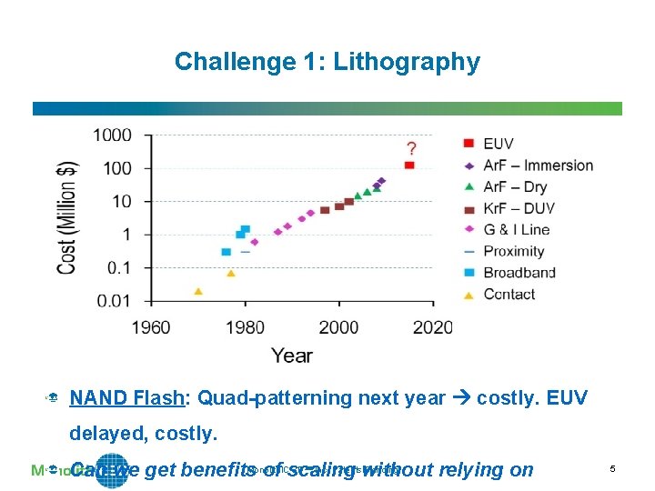
Challenge 1: Lithography NAND Flash: Quad-patterning next year costly. EUV delayed, costly. Monolith. IC 3 D Inc. Patentswithout Pending Can we get benefits of scaling relying on 5
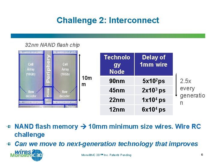
Challenge 2: Interconnect 32 nm NAND flash chip 10 m m Technolo gy Node Delay of 1 mm wire 90 nm 5 x 10² ps 45 nm 2 x 10³ ps 22 nm 1 x 10⁴ ps 12 nm 6 x 10⁴ ps 2. 5 x every generatio n NAND flash memory 10 mm minimum size wires. Wire RC challenge Can we move to next-generation technology that improves wires? 6 Monolith. IC 3 D Inc. Patents Pending
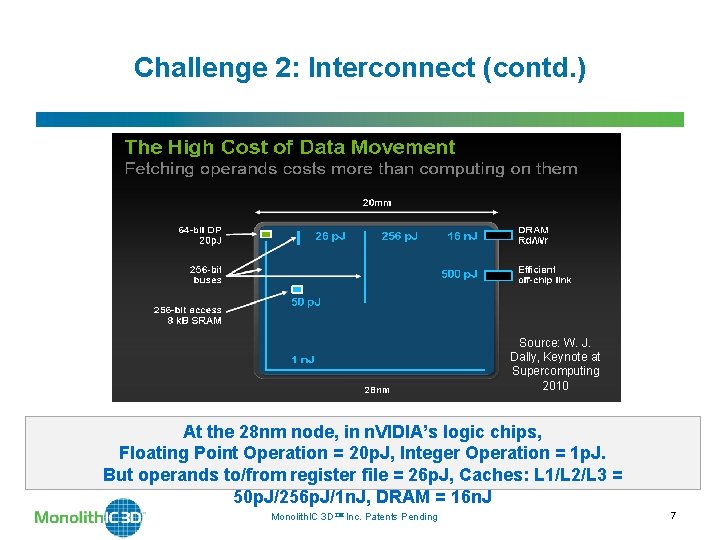
Challenge 2: Interconnect (contd. ) Source: W. J. Dally, Keynote at Supercomputing 2010 At the 28 nm node, in n. VIDIA’s logic chips, Floating Point Operation = 20 p. J, Integer Operation = 1 p. J. But operands to/from register file = 26 p. J, Caches: L 1/L 2/L 3 = 50 p. J/256 p. J/1 n. J, DRAM = 16 n. J Monolith. IC 3 D Inc. Patents Pending 7
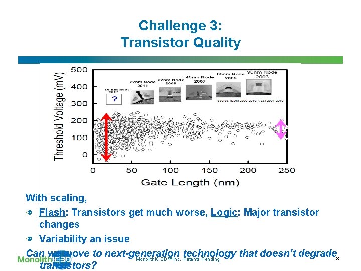
Challenge 3: Transistor Quality With scaling, Flash: Transistors get much worse, Logic: Major transistor changes Variability an issue Can we move to next-generation technology that doesn’t degrade 8 Monolith. IC 3 D Inc. Patents Pending transistors?
How to get stacked single crystal silicon layers Monolith. IC 3 D Inc. Patents Pending 9
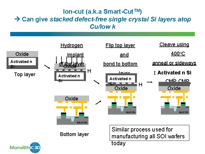
Ion-cut (a. k. a Smart-Cut. TM) Can give stacked defect-free single crystal Si layers atop Cu/low k Hydrogen Oxide Activated n Si Top layer implant of. Oxide top layer Activated n Si Cleave using Flip top layer 400 o. C and anneal or sideways bond to bottom H mechanical Activated force. n Si layer Activated n Si Oxide H CMP. Oxide Bottom layer Similar process used for manufacturing all SOI wafers today
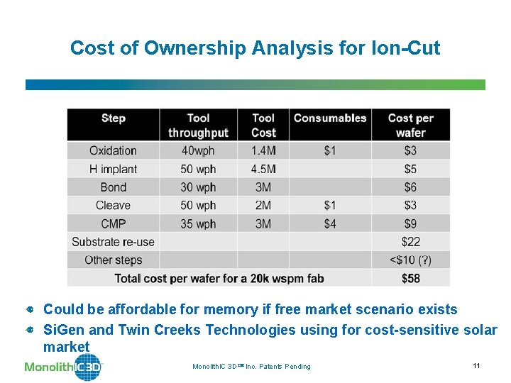
Cost of Ownership Analysis for Ion-Cut Could be affordable for memory if free market scenario exists Si. Gen and Twin Creeks Technologies using for cost-sensitive solar market Monolith. IC 3 D Inc. Patents Pending 11
Monolithic 3 D NAND Flash Memory USP: Single-crystal silicon vs. poly Si for rest of industry Monolith. IC 3 D Inc. Patents Pending 12
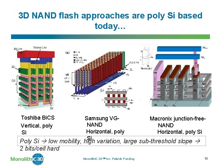
3 D NAND flash approaches are poly Si based today… Toshiba Bi. CS Vertical, poly Si Samsung VGNAND Horizontal, poly Si Macronix junction-free. NAND Horizontal, poly Si Poly Si low mobility, high variation, large sub-threshold slope 2 bits/cell hard Monolith. IC 3 D Inc. Patents Pending 13
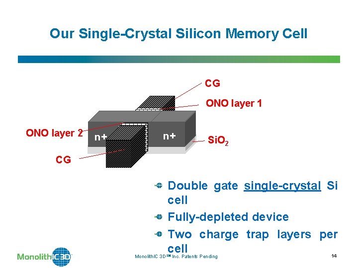
Our Single-Crystal Silicon Memory Cell CG n+ ONO layer 1 ONO layer 2 n+ n+ Si. O 2 CG Double gate single-crystal Si cell Fully-depleted device Two charge trap layers per cell 14 Monolith. IC 3 D Inc. Patents Pending
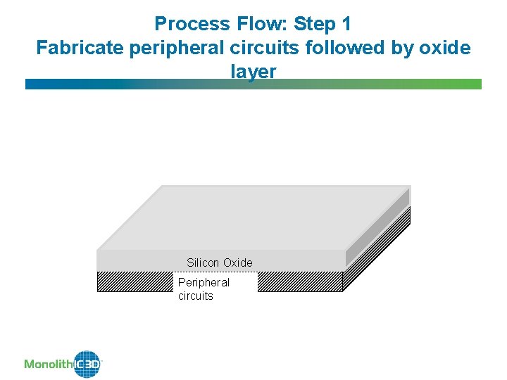
Process Flow: Step 1 Fabricate peripheral circuits followed by oxide layer Silicon Oxide Peripheral circuits
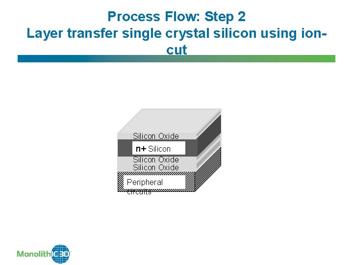
Process Flow: Step 2 Layer transfer single crystal silicon using ioncut Silicon Oxide n+ Silicon Oxide Peripheral circuits
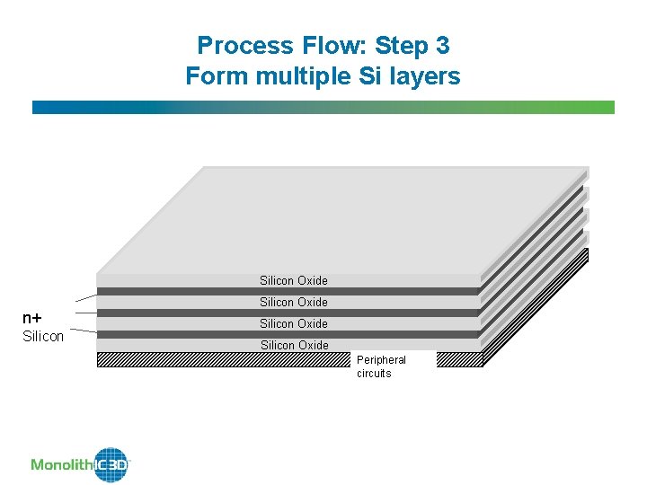
Process Flow: Step 3 Form multiple Si layers Silicon Oxide 06 Silicon Oxide n+ Silicon Oxide Peripheral circuits
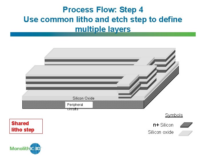
Process Flow: Step 4 Use common litho and etch step to define multiple layers Silicon Oxide 06 Silicon Oxide 06 Silicon Oxide Peripheral circuits Symbols Shared litho step n+ Silicon oxide
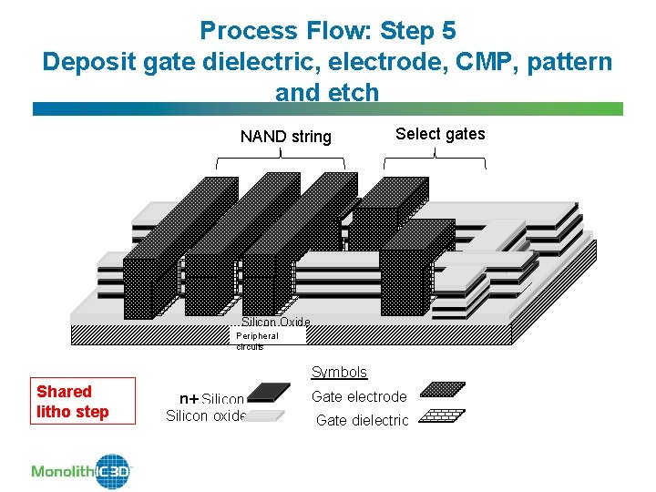
Process Flow: Step 5 Deposit gate dielectric, electrode, CMP, pattern and etch NAND string Select gates Silicon Oxide 06 Silicon Oxide 06 Silicon Oxide Peripheral circuits Symbols Shared litho step n+ Silicon oxide Gate electrode 3724 Gate dielectric
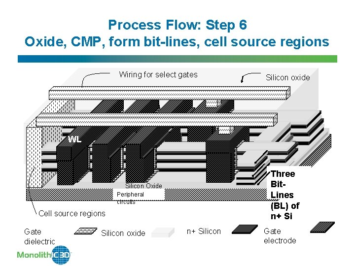
Process Flow: Step 6 Oxide, CMP, form bit-lines, cell source regions Wiring for select gates Silicon Oxide 06 WL Silicon Oxide 06 Three Bit. Lines (BL) of n+ Si Silicon Oxide Peripheral circuits Cell source regions Gate dielectric Silicon oxide n+ Silicon Gate electrode
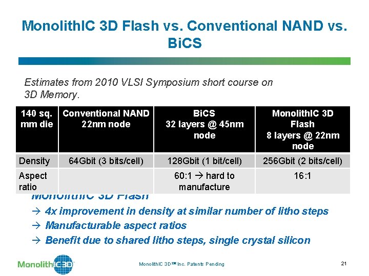
Monolith. IC 3 D Flash vs. Conventional NAND vs. Bi. CS Estimates from 2010 VLSI Symposium short course on 3 D Memory. 140 sq. mm die Conventional NAND 22 nm node Bi. CS 32 layers @ 45 nm node Monolith. IC 3 D Flash 8 layers @ 22 nm node Density 64 Gbit (3 bits/cell) 128 Gbit (1 bit/cell) 256 Gbit (2 bits/cell) 60: 1 hard to manufacture 16: 1 Aspect ratio Monolith. IC 3 D Flash 4 x improvement in density at similar number of litho steps Manufacturable aspect ratios Benefit due to shared litho steps, single crystal silicon Monolith. IC 3 D Inc. Patents Pending 21
Monolithic 3 D DRAM, Resistive Memories Shared litho architectures enabled by c-Si stacking Monolith. IC 3 D Inc. Patents Pending 22
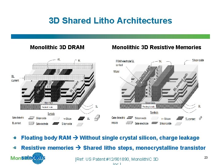
3 D Shared Litho Architectures Monolithic 3 D DRAM Monolithic 3 D Resistive Memories Floating body RAM Without single crystal silicon, charge leakage Resistive memories Shared litho steps, monocrystalline transistor selectors [Ref: US Patent #12/901890, Monolith. IC 3 D 23
Monolithic 3 D Logic USP: Shorter wires. So, gates driving wires smaller. Monolith. IC 3 D Inc. Patents Pending 24
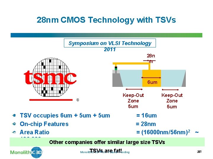
28 nm CMOS Technology with TSVs Symposium on VLSI Technology 2011 28 n m 6 um Keep-Out Zone 5 um TSV occupies 6 um + 5 um = 16 um On-chip Features = 28 nm Area Ratio = (16000 nm/56 nm) 2 ~ 100, 000 x Other companies offer similar large size TSVs are fat! Monolith. IC 3 D Inc. Patents Pending 25 25
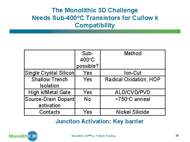
The Monolithic 3 D Challenge Needs Sub-400 o. C Transistors for Cu/low k Compatibility Sub 400 o. C possible? Single Crystal Silicon Yes Shallow Trench Yes Isolation High k/Metal Gate Yes Source-Drain Dopant No activation Contacts Yes Method Ion-Cut Radical Oxidation, HDP ALD/CVD/PVD >750 o. C anneal Nickel Silicide Junction Activation: Key barrier Monolith. IC 3 D Inc. Patents Pending 26
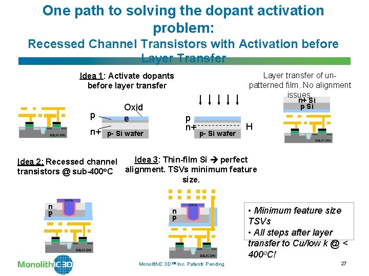
One path to solving the dopant activation problem: Recessed Channel Transistors with Activation before Layer Transfer Layer transfer of unpatterned film. No alignment issues. Idea 1: Activate dopants before layer transfer p n+ n+ Si p Si Oxid e p n+ p- Si wafer H Idea 3: Thin-film Si perfect Idea 2: Recessed channel transistors @ sub-400 o. C alignment. TSVs minimum feature size. n p + Monolith. IC 3 D Inc. Patents Pending • Minimum feature size TSVs • All steps after layer transfer to Cu/low k @ < 400 o. C! 27
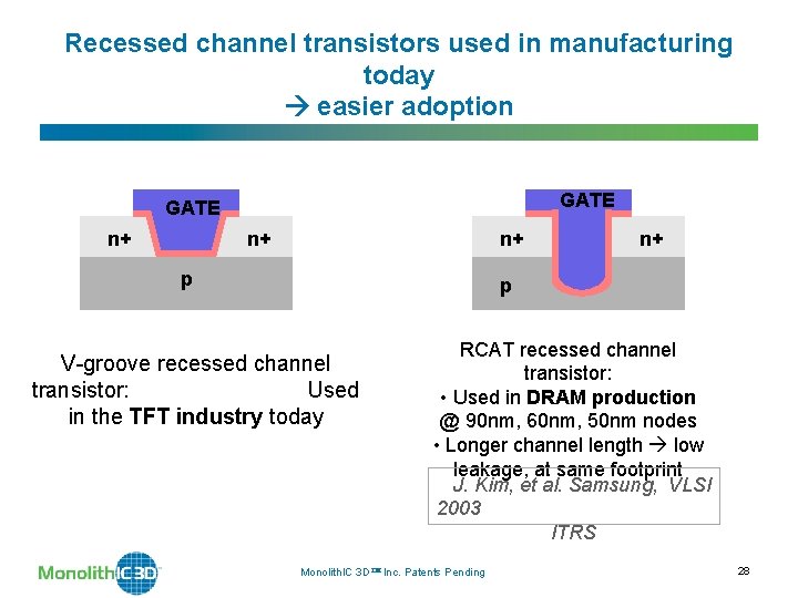
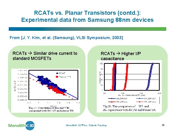
Recessed channel transistors used in manufacturing today easier adoption GATE n+ n+ n+ p GATE GAT E n+ p V-groove recessed channel transistor: Used in the TFT industry today RCAT recessed channel transistor: • Used in DRAM production @ 90 nm, 60 nm, 50 nm nodes • Longer channel length low leakage, at same footprint J. Kim, et al. Samsung, VLSI 2003 ITRS Monolith. IC 3 D Inc. Patents Pending 28
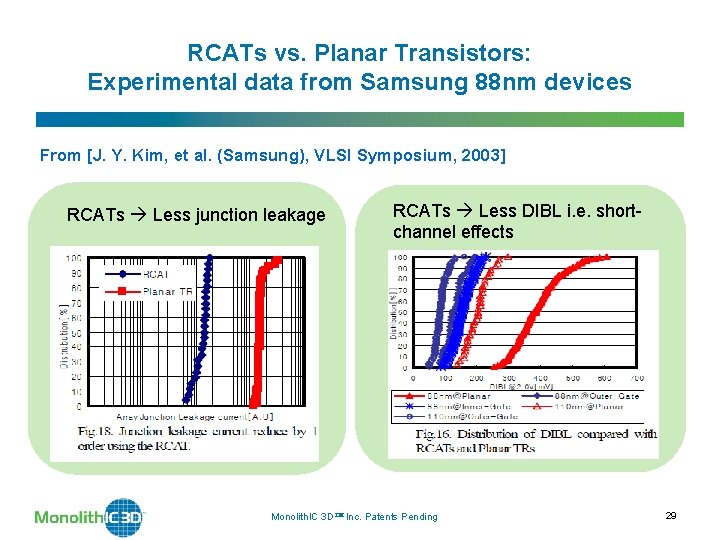
RCATs vs. Planar Transistors: Experimental data from Samsung 88 nm devices From [J. Y. Kim, et al. (Samsung), VLSI Symposium, 2003] RCATs Less junction leakage RCATs Less DIBL i. e. shortchannel effects Monolith. IC 3 D Inc. Patents Pending 29
RCATs vs. Planar Transistors (contd. ): Experimental data from Samsung 88 nm devices From [J. Y. Kim, et al. (Samsung), VLSI Symposium, 2003] RCATs Similar drive current to standard MOSFETs RCATs Higher I/P capacitance Monolith. IC 3 D Inc. Patents Pending 30
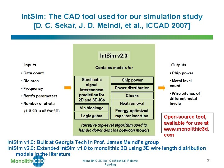
Int. Sim: The CAD tool used for our simulation study [D. C. Sekar, J. D. Meindl, et al. , ICCAD 2007] Open-source tool, available for use at www. monolithic 3 d. com Int. Sim v 1. 0: Built at Georgia Tech in Prof. James Meindl’s group Int. Sim v 2. 0: Extended Int. Sim v 1. 0 to monolithic 3 D using 3 D wire length distribution models in the literature Monolith. IC 3 D Inc. Confidential, Patents Pending 31
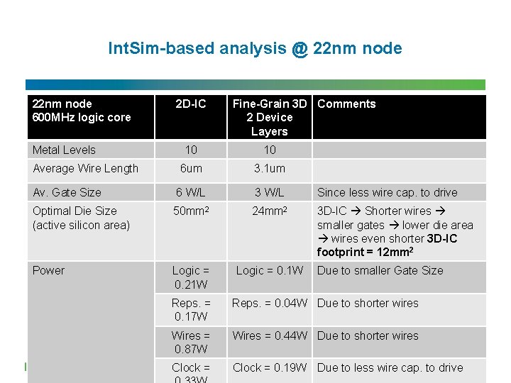
Int. Sim-based analysis @ 22 nm node 600 MHz logic core Metal Levels 2 D-IC Fine-Grain 3 D Comments 2 Device Layers 10 10 6 um 3. 1 um Av. Gate Size 6 W/L 3 W/L Since less wire cap. to drive Optimal Die Size (active silicon area) 50 mm 2 24 mm 2 3 D-IC Shorter wires smaller gates lower die area wires even shorter 3 D-IC footprint = 12 mm 2 Power Logic = 0. 21 W Logic = 0. 1 W Average Wire Length Reps. = 0. 17 W Due to smaller Gate Size Reps. = 0. 04 W Due to shorter wires Wires = 0. 44 W Due to shorter wires 3 D with sub-50 nm TSVs 2 x lower power, 2 x lower active silicon area 0. 87 W Monolith. IC 3 D Inc. Patents Pending Due to less wire cap. to drive Clock = 0. 19 W 32
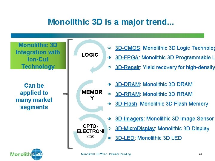
Monolithic 3 D is a major trend. . . Monolithic 3 D Integration with Ion-Cut Technology Can be applied to many market segments 3 D-CMOS: Monolithic 3 D Logic Technolog LOGIC 3 D-FPGA: Monolithic 3 D Programmable L 3 D-Repair: Yield recovery for high-density 3 D-DRAM: Monolithic 3 D DRAM MEMOR Y 3 D-RRAM: Monolithic 3 D RRAM 3 D-Flash: Monolithic 3 D Flash Memory 3 D-Imagers: Monolithic 3 D Image Sensor OPTOELECTRONI CS 3 D-Micro. Display: Monolithic 3 D Display 3 D-LED: Monolithic 3 D LED Monolith. IC 3 D Inc. Patents Pending 33
Summary Monolith. IC 3 D Inc. Patents Pending 34
To summarize. . Monolithic 3 D attractive for logic, flash, DRAM and many other applications Benefits: Logic – Short wires, Smaller gates to drive wires. Less power and area Memory – Shared litho steps, short wires Risks: Competing with 2 D NAND roadmap, CAD Tools, transistor optimization, etc Increasingly attractive due to lithography, interconnect trends Monolith. IC 3 D Inc. Patents Pending 35
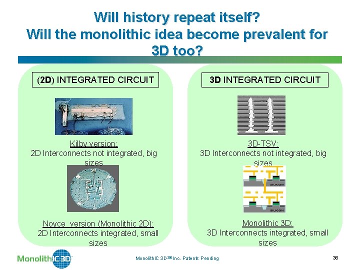
Will history repeat itself? Will the monolithic idea become prevalent for 3 D too? (2 D) INTEGRATED CIRCUIT 3 D INTEGRATED CIRCUIT Kilby version: 2 D Interconnects not integrated, big sizes 3 D-TSV: 3 D Interconnects not integrated, big sizes Noyce version (Monolithic 2 D): 2 D Interconnects integrated, small sizes Monolithic 3 D: 3 D Interconnects integrated, small sizes Monolith. IC 3 D Inc. Patents Pending 36
Acknowledgements Brian Cronquist, Israel Beinglass, Ze’ev Wurman, Iulia Morariu, Andrei Dalcu, Paul Lim, Parthiv Mohan – all with Monolith. IC 3 D Inc. Patents Pending 37
Thank you Monolith. IC 3 D Inc. Patents Pending 38
Backup slides Monolith. IC 3 D Inc. Patents Pending 39
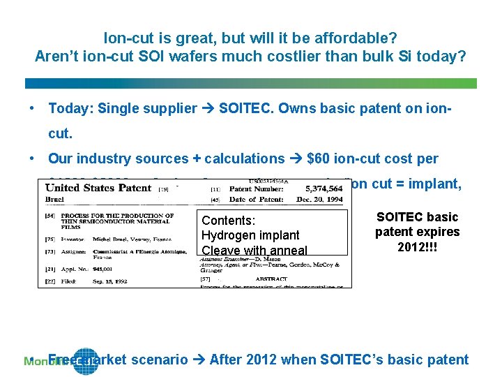
Ion-cut is great, but will it be affordable? Aren’t ion-cut SOI wafers much costlier than bulk Si today? • Today: Single supplier SOITEC. Owns basic patent on ioncut. • Our industry sources + calculations $60 ion-cut cost per $1500 -$5000 wafer in a free market scenario (ion cut = implant, bond, anneal). Contents: Hydrogen implant Cleave with anneal SOITEC basic patent expires 2012!!! • Free market scenario After 2012 when SOITEC’s basic patent
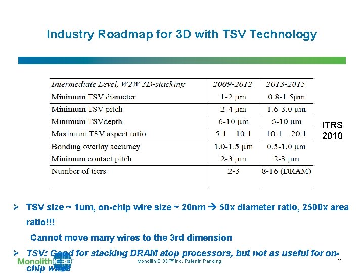
Industry Roadmap for 3 D with TSV Technology ITRS 2010 Ø TSV size ~ 1 um, on-chip wire size ~ 20 nm 50 x diameter ratio, 2500 x area ratio!!! Cannot move many wires to the 3 rd dimension Ø TSV: Good for stacking DRAM atop processors, but not as useful for onchip wires Monolith. IC 3 D Inc. Patents Pending 41
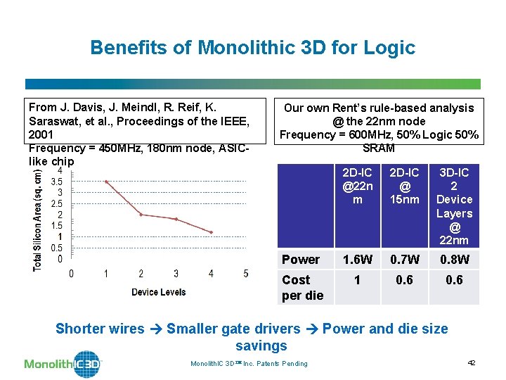
Benefits of Monolithic 3 D for Logic From J. Davis, J. Meindl, R. Reif, K. Saraswat, et al. , Proceedings of the IEEE, 2001 Frequency = 450 MHz, 180 nm node, ASIClike chip Our own Rent’s rule-based analysis @ the 22 nm node Frequency = 600 MHz, 50% Logic 50% SRAM 2 D-IC @22 n m 2 D-IC @ 15 nm 3 D-IC 2 Device Layers @ 22 nm Power 1. 6 W 0. 7 W 0. 8 W Cost per die 1 0. 6 Shorter wires Smaller gate drivers Power and die size savings Monolith. IC 3 D Inc. Patents Pending 42
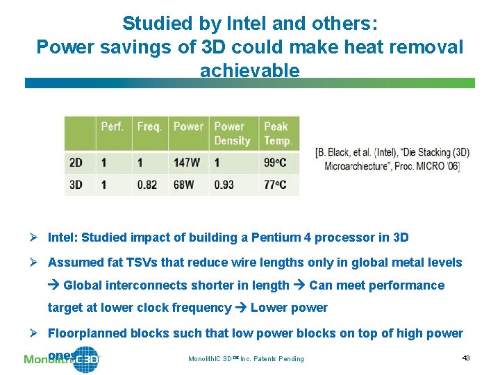
Studied by Intel and others: Power savings of 3 D could make heat removal achievable Ø Intel: Studied impact of building a Pentium 4 processor in 3 D Ø Assumed fat TSVs that reduce wire lengths only in global metal levels Global interconnects shorter in length Can meet performance target at lower clock frequency Lower power Ø Floorplanned blocks such that low power blocks on top of high power ones Monolith. IC 3 D Inc. Patents Pending 43
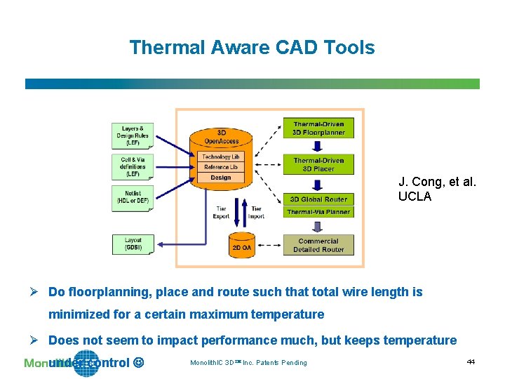
Thermal Aware CAD Tools J. Cong, et al. UCLA Ø Do floorplanning, place and route such that total wire length is minimized for a certain maximum temperature Ø Does not seem to impact performance much, but keeps temperature under control Monolith. IC 3 D Inc. Patents Pending 44
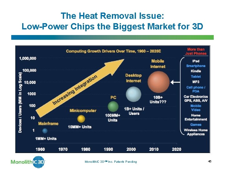
The Heat Removal Issue: Low-Power Chips the Biggest Market for 3 D Monolith. IC 3 D Inc. Patents Pending 45
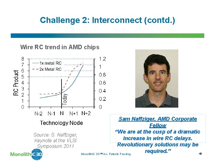
Challenge 2: Interconnect (contd. ) Wire RC trend in AMD chips Sam Naffziger, AMD Corporate Fellow “We are at the cusp of a dramatic Source: S. Naffziger, increase in wire RC delays. Keynote at the VLSI Revolutionary solutions may be Symposium 2011 required. ” 46 Monolith. IC 3 D Inc. Patents Pending