Monolith IC 3 D ICs HKMG Gate Last
- Slides: 11

Monolith. IC 3 D ICs HKMG – Gate Last - Flow Monolith. IC 3 D Inc. , Patents Pending 1

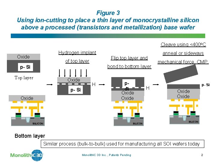
Figure 3 Using ion-cutting to place a thin layer of monocrystalline silicon above a processed (transistors and metallization) base wafer Cleave using <400 o. C Hydrogen implant Oxide Flip top layer and of top layer bond to bottom layer p- Si Top layer Oxide p- Si Oxide H p. Si Oxide H anneal or sideways mechanical force. CMP. p- Si Oxide Bottom layer Similar process (bulk-to-bulk) used for manufacturing all SOI wafers today Monolith. IC 3 D Inc. , Patents Pending 2

Monolithic 3 D ICs Using Smart. Cut technology - the ion cutting process that Soitec uses to make SOI wafers for AMD and IBM (million of wafers had utilized the process over the last 20 years) - to stack up consecutive layers of active silicon (bond first and then cut). Soitec’s Smart Cut Patented* Flow (access link for video). *Soitec’s fundamental patent US 5, 374, 564 expired Sep. 15, 2012 Monolith. IC 3 D Inc. , Patents Pending 3

Monolithic 3 D ICs Ion cutting: the key idea is that if you implant a thin layer of H+ ions into a single crystal of silicon, the ions will weaken the bonds between the neighboring silicon atoms, creating a fracture plane (Figure 3). Judicious force will then precisely break the wafer at the plane of the H+ implant, allowing you to in effect peel off very thin layer. This technique is currently being used to produce the most advanced transistors (Fully Depleted SOI, UTBB transistors – Ultra Thin Body and BOX), forming monocrystalline silicon layers that are less than 10 nm thick. Monolith. IC 3 D Inc. , Patents Pending 4

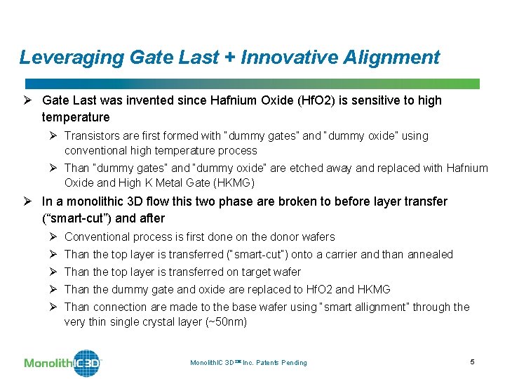
Leveraging Gate Last + Innovative Alignment Ø Gate Last was invented since Hafnium Oxide (Hf. O 2) is sensitive to high temperature Ø Transistors are first formed with “dummy gates” and “dummy oxide” using conventional high temperature process Ø Than “dummy gates” and “dummy oxide” are etched away and replaced with Hafnium Oxide and High K Metal Gate (HKMG) Ø In a monolithic 3 D flow this two phase are broken to before layer transfer (“smart-cut”) and after Ø Conventional process is first done on the donor wafers Ø Than the top layer is transferred (“smart-cut”) onto a carrier and than annealed Ø Than the top layer is transferred on target wafer Ø Than the dummy gate and oxide are replaced to Hf. O 2 and HKMG Ø Than connection are made to the base wafer using “smart allignment” through the very thin single crystal layer (~50 nm) Monolith. IC 3 D Inc. Patents Pending 5

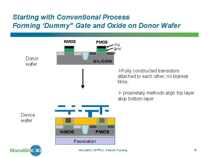
Starting with Conventional Process Forming ‘Dummy” Gate and Oxide on Donor Wafer NMOS Pol Oxid y e Donor wafer ØFully constructed transistors attached to each other; no blanket films. Ø proprietary methods align top layer atop bottom layer Device wafer Monolith. IC 3 D Inc. Patents Pending 6

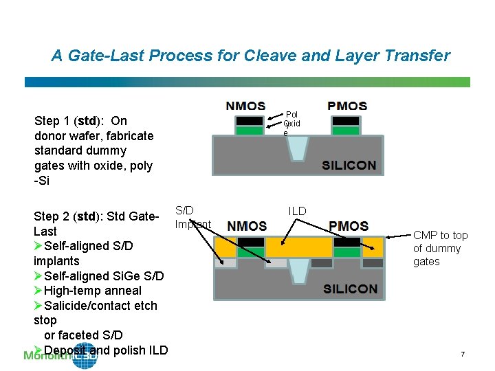
A Gate-Last Process for Cleave and Layer Transfer Step 1 (std): On donor wafer, fabricate standard dummy gates with oxide, poly -Si Step 2 (std): Std Gate- S/D Implant Last ØSelf-aligned S/D implants ØSelf-aligned Si. Ge S/D ØHigh-temp anneal ØSalicide/contact etch stop or faceted S/D ØDeposit and polish ILD Pol Oxid y e ILD CMP to top of dummy gates 7

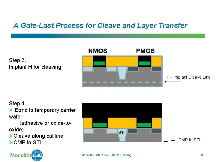
A Gate-Last Process for Cleave and Layer Transfer Step 3. Implant H for cleaving H+ Implant Cleave Line Step 4. Ø Bond to temporary carrier wafer (adhesive or oxide-tooxide) ØCleave along cut line ØCMP to STI Carrier STI CMP to STI Monolith. IC 3 D Inc. Patents Pending 8

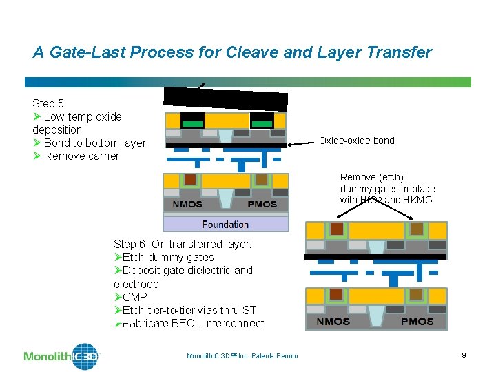
A Gate-Last Process for Cleave and Layer Transfer Step 5. Ø Low-temp oxide deposition Ø Bond to bottom layer Ø Remove carrier Carrier Oxide-oxide bond Remove (etch) dummy gates, replace with Hf. O 2 and HKMG Step 6. On transferred layer: ØEtch dummy gates ØDeposit gate dielectric and electrode ØCMP ØEtch tier-to-tier vias thru STI ØFabricate BEOL interconnect Monolith. IC 3 D Inc. Patents Pending 9

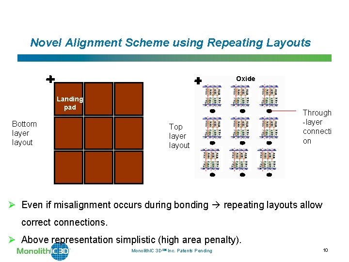
Novel Alignment Scheme using Repeating Layouts Oxide Landing pad Bottom layer layout Top layer layout Through -layer connecti on Ø Even if misalignment occurs during bonding repeating layouts allow correct connections. Ø Above representation simplistic (high area penalty). Monolith. IC 3 D Inc. Patents Pending 10

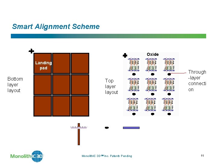
Smart Alignment Scheme Oxide Landing pad Bottom layer layout Top layer layout Monolith. IC 3 D Inc. Patents Pending Through -layer connecti on 11