Module3 DataProcessing Circuits and Flip Flops 1 Books
Module-3 Data-Processing Circuits and Flip- Flops 1
Books Referred • Donald P Leach, Albert Paul Malvino & Goutam Saha: Digital Principles and Applications, 7 th Edition, Tata Mc. Graw Hill, 2015 • Stephen Brown, Zvonko Vranesic: Fundamentals of Digital Logic Design with VHDL, 2 nd Edition, Tata Mc. Graw Hill, 2005. 2
Objectives • Determine the output of a multiplexer or demultiplexer based on input conditions. • Find, based on input conditions, the output of an encoder or decoder. • Draw the symbol and write the truth table for an exclusive-OR gate. • Explain the purpose of parity checking. • Show a magnitude comparator works. • Describe a PAL and PLA. • Describe the half-adder, full-adder, and adder-subtractor. • Describe how an Arithmetic Logic Unit can be operated. • Describe the operation of the basic RS flip-flop and explain the purpose of the additional input on the gated (clocked) RS flip-flop. • Show the truth table for the edge-triggered. RS flip-flop, edgetriggered D flip-flop and edge-triggered JK flip-flop. 3
DATA-PROCESSING CIRCUITS 4
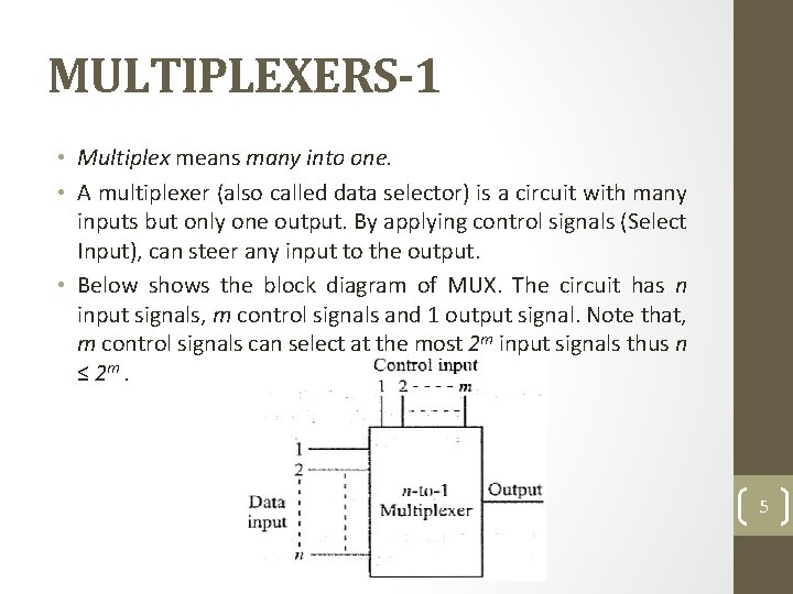
MULTIPLEXERS-1 • Multiplex means many into one. • A multiplexer (also called data selector) is a circuit with many inputs but only one output. By applying control signals (Select Input), can steer any input to the output. • Below shows the block diagram of MUX. The circuit has n input signals, m control signals and 1 output signal. Note that, m control signals can select at the most 2 m input signals thus n ≤ 2 m. 5
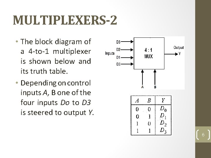
MULTIPLEXERS-2 • The block diagram of a 4 -to-1 multiplexer is shown below and its truth table. • Depending on control inputs A, B one of the four inputs Do to D 3 is steered to output Y. 6
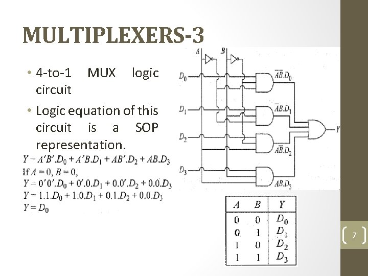
MULTIPLEXERS-3 • 4 -to-1 MUX logic circuit • Logic equation of this circuit is a SOP representation. 7
MULTIPLEXERS-4 • In other words, for AB = 00, the first AND gate to which D 0 is connected remains active and equal to Do and all other AND gate are inactive with output held at logic 0. • Thus, multiplexer output Y is same as D 0. If D 0 =0, Y=0 and if D 0 = 1, Y= 1. • Commercial multiplexers ICs come in integer power of 2, e. g. 2 -to-1, 4 -to-1, 8 -to- 1, 16 -to-1 multiplexers. • Write the 2 to 1 MUX block diagram, equation and it truth table. 8
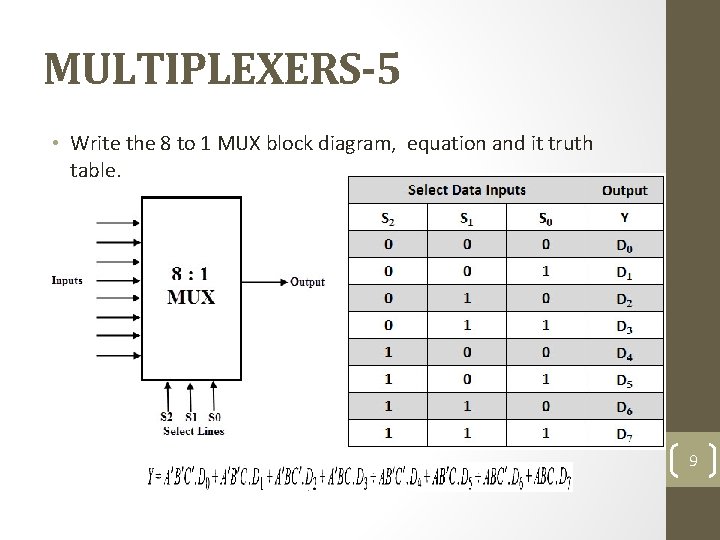
MULTIPLEXERS-5 • Write the 8 to 1 MUX block diagram, equation and it truth table. 9
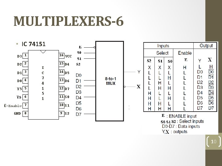
MULTIPLEXERS-6 • IC 74151 D 3 1 16 VCC D 2 2 15 D 4 D 1 3 D 0 4 Y 5 5 6 I C 7 4 1 5 1 14 D 5 13 D 6 12 D 7 11 S 0 7 10 S 1 GND 8 9 S 2 10
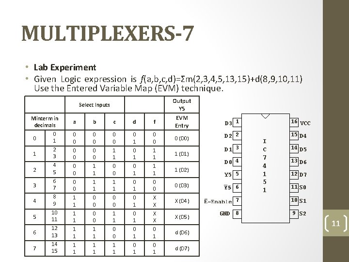
MULTIPLEXERS-7 • Lab Experiment • Given Logic expression is f(a, b, c, d)=Σm(2, 3, 4, 5, 13, 15)+d(8, 9, 10, 11) Use the Entered Variable Map (EVM) technique. Output Y 5 Select Inputs a b c d f EVM Entry D 3 1 0 0 0 0 1 0 0 0 (D 0) D 2 2 1 2 3 0 0 1 1 (D 1) 2 4 5 0 0 1 1 0 0 0 1 1 (D 2) 3 6 7 0 0 1 1 0 1 0 0 0 (D 3) 6 4 8 9 1 1 0 0 0 1 X X X (D 4) 7 10 S 1 5 10 11 1 1 0 0 1 1 0 1 X X X (D 5) GND 8 9 S 2 6 12 13 1 1 0 0 0 1 d (D 6) 7 14 15 1 1 1 0 1 d (D 7) Minterm in decimals 0 0 1 D 1 3 D 0 4 Y 5 5 16 VCC I C 7 4 1 5 1 15 D 4 14 D 5 13 D 6 12 D 7 11 S 0 11
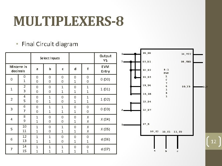
MULTIPLEXERS-8 • Final Circuit diagram Output Y 5 Select Inputs Minterm in decimals 0 0 1 a b c d f EVM Entry 0 0 0 0 1 0 0 0 (D 0) 1 2 3 0 0 1 1 (D 1) 2 4 5 0 0 1 1 0 0 0 1 1 (D 2) 3 6 7 0 0 1 1 0 1 0 0 0 (D 3) 4 8 9 1 1 0 0 0 1 X X X (D 4) 5 10 11 1 1 0 0 1 1 0 1 X X X (D 5) 6 12 13 1 1 0 0 0 1 d (D 6) 7 14 15 1 1 1 0 1 d (D 7) 0 04, D 0 16, VCC 1 03, D 1 08, GND 8: 1 MUX I C 7 4 1 5 1 02, D 2 01, D 3 15, D 4 14, D 5 05, Y 5 O/P 13, D 6 d 12, D 7 0 07, E 09, S 2 10, S 1 11, S 0 12 a b c
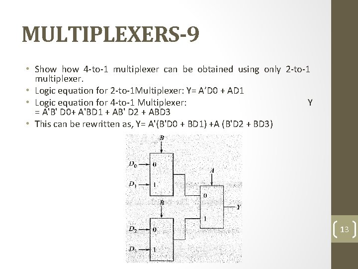
MULTIPLEXERS-9 • Show 4 -to-1 multiplexer can be obtained using only 2 -to-1 multiplexer. • Logic equation for 2 -to-1 Multiplexer: Y= A’D 0 + AD 1 • Logic equation for 4 -to-1 Multiplexer: Y = A'B' D 0+ A'BD 1 + AB' D 2 + ABD 3 • This can be rewritten as, Y= A'(B'D 0 + BD 1) +A (B'D 2 + BD 3) 13
MULTIPLEXERS-10 • Realize Y=A'B + B'C' + ABC using an 8 -to-1 multiplexer. • First we express Y as a function of minterms of three variables. Thus • Y = A'B + B'C' + ABC • Y =A'B(C' + C)+B'C'(A' + A)+ ABC [As, X+X'= I] • Y = A'B'C' + A'BC + AB'C' + ABC • Comparing this with equation of 8 to 1 multiplexer, we find by substituting D 0 = D 2 = D 3 =D 4 = D 1 = 1 and D 1 = D 5 = D 6 = 0. 14
MULTIPLEXERS-11 • Can it be realized above equation with a 4 -to-1 multiplexer? • The 4 -to-1 multiplexer generates 4 minterms for different combinations of AB. We rewrite given logic equation in such a way that all these terms are present in the equation. • Y =A'B+B'C' +ABC • Y =A'B+ B'C'(A' +A)+ ABC [As, X +X' = I] • Y =A'B'. C' + A'B. 1 +AB'. C' + AB. C • Compare above with equation of a 4 -to-1 multiplexer. We see D 0= C', D 1 = 1, D 2 = C' and. D 3 = C generate the given logic function. 15
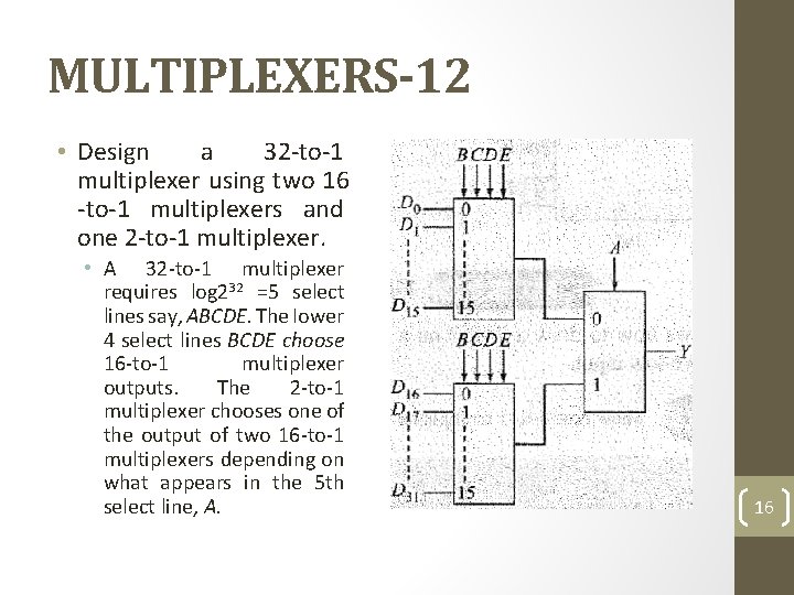
MULTIPLEXERS-12 • Design a 32 -to-1 multiplexer using two 16 -to-1 multiplexers and one 2 -to-1 multiplexer. • A 32 -to-1 multiplexer requires log 232 =5 select lines say, ABCDE. The Iower 4 select lines BCDE choose 16 -to-1 multiplexer outputs. The 2 -to-1 multiplexer chooses one of the output of two 16 -to-1 multiplexers depending on what appears in the 5 th select line, A. 16
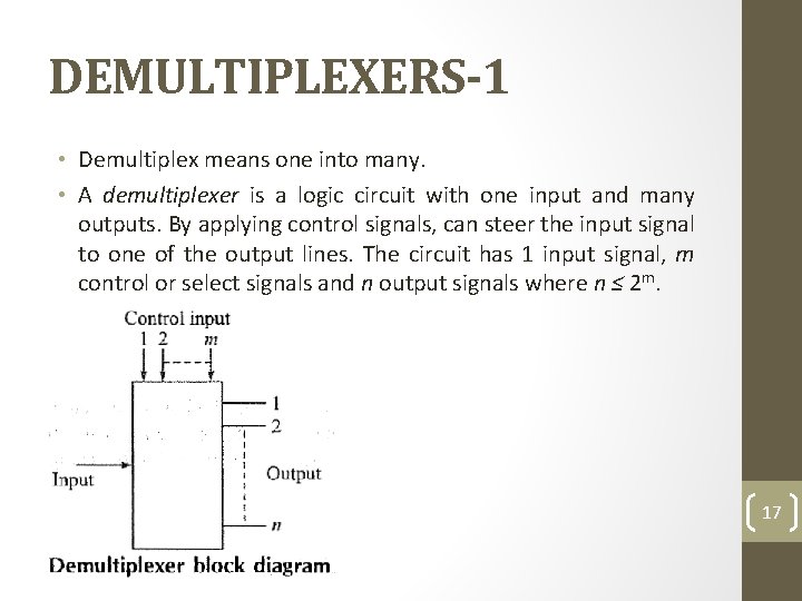
DEMULTIPLEXERS-1 • Demultiplex means one into many. • A demultiplexer is a logic circuit with one input and many outputs. By applying control signals, can steer the input signal to one of the output lines. The circuit has 1 input signal, m control or select signals and n output signals where n ≤ 2 m. 17
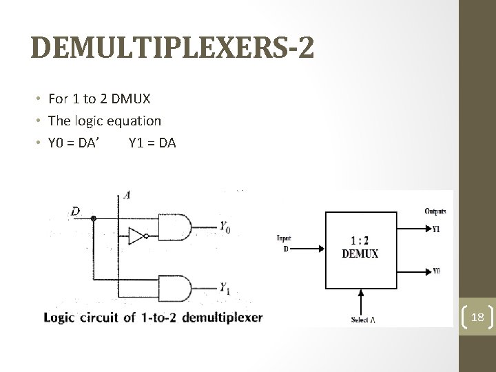
DEMULTIPLEXERS-2 • For 1 to 2 DMUX • The logic equation • Y 0 = DA’ Y 1 = DA 18
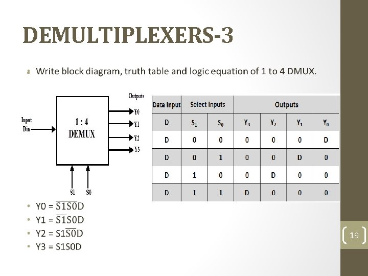
DEMULTIPLEXERS-3 • 19

DEMULTIPLEXERS-4 • Write block diagram, truth table and log equation of 1 to 8 DMUX. 20
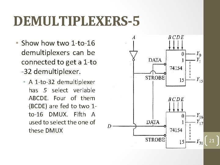
DEMULTIPLEXERS-5 • Show two 1 -to-16 demultiplexers can be connected to get a 1 -to -32 demultiplexer. • A 1 -to-32 demultiplexer has 5 select veriable ABCDE. Four of them (BCDE) are fed to two 1 to-16 DMUX. Fifth A used to select the one of these DMUX 21
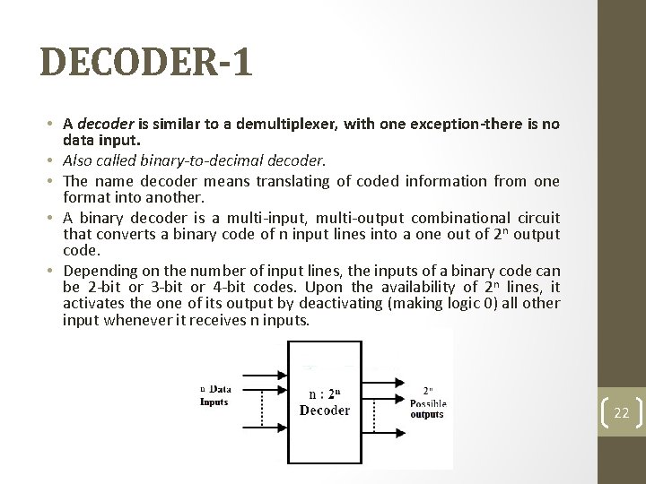
DECODER-1 • A decoder is similar to a demultiplexer, with one exception-there is no data input. • Also called binary-to-decimal decoder. • The name decoder means translating of coded information from one format into another. • A binary decoder is a multi-input, multi-output combinational circuit that converts a binary code of n input lines into a one out of 2 n output code. • Depending on the number of input lines, the inputs of a binary code can be 2 -bit or 3 -bit or 4 -bit codes. Upon the availability of 2 n lines, it activates the one of its output by deactivating (making logic 0) all other input whenever it receives n inputs. 22
DECODER-2 • The most commonly used practical binary decoders are 2 -to-4 decoder, 3 -to-8 decoder and 4 -to-16 line binary decoder. • 2 -to-4 decoder also called 1 of 4 • 3 -to-8 decoder also called 1 of 8 • 4 -to-16 line binary decoder also called 1 of 16 23
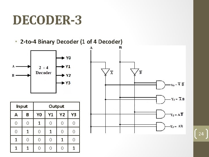
DECODER-3 • 2 -to-4 Binary Decoder (1 of 4 Decoder) Input Output A B Y 0 Y 1 Y 2 Y 3 0 0 1 0 0 1 0 0 0 1 24
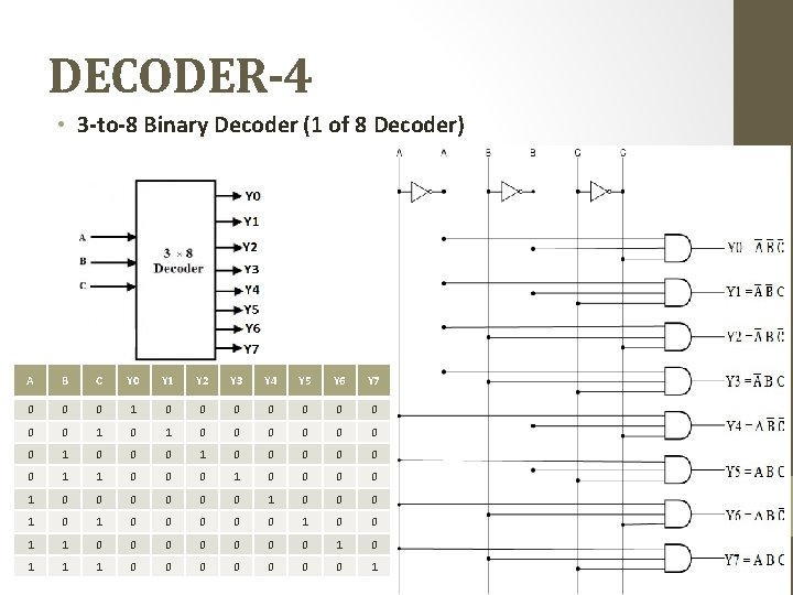
DECODER-4 • 3 -to-8 Binary Decoder (1 of 8 Decoder) A B C Y 0 Y 1 Y 2 Y 3 Y 4 Y 5 Y 6 Y 7 0 0 0 1 0 0 0 0 1 0 0 0 0 1 0 0 0 1 0 0 0 1 1 0 0 0 0 1 1 1 0 0 0 0 1 25
DECODER-5 • Similarly for 4 to 16 or 1 of 16 Decoder 26
DECODER-6 • Applications of Decoders • Decoders are greatly used in applications where the particular output or group of outputs to be activated only on the occurrence of a specific combination of input levels. • Binary to Decimal Decoder • Decoders are used to get the decimal digit corresponding to a specific input combination. A BCD number needs 4 binary digits to represent the 0 to 9 decimal digits, thus it consists of 4 input lines. It consists of 10 output lines corresponding to 0 to 9 decimal digits. (1 of 10 line decoder) • Address Decoders • Amongst its many uses, a decoder is widely used to decode the particular memory location in the computer memory system. Decoders accept the address code generated by the CPU which is a combination of address bits for a specific location in the memory. In a memory system, there are several memory ICs are combined and each one has their unique address to distinguish from other memory locations. In such cases a decoder built in the memory ICs circuitry, is used to select a memory IC in response to a range of addresses by decoding the most significant bits of the systems address, thereby a particular memory location or IC is selected. • Instruction Decoder • Another application of the decoder can be found in the control unit of the central processing unit. This decoder is used to decode the program instructions in order to activate the specific control lines such that different operations in the ALU of the CPU are carried out. 27
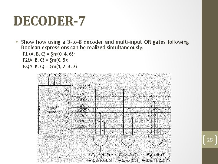
DECODER-7 • Show using a 3 -to-8 decoder and multi-input OR gates following Boolean expressions can be realized simultaneously. F 1 (A, B, C) = ∑m(0, 4, 6); F 2(A, B, C) = ∑m(0, 5); F 3(A, B, C) = ∑m(1, 2, 3, 7) 28
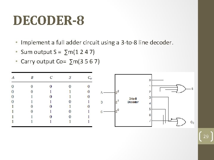
DECODER-8 • Implement a full adder circuit using a 3 -to-8 line decoder. • Sum output S = ∑m(1 2 4 7) • Carry output Co= ∑m(3 5 6 7) 29
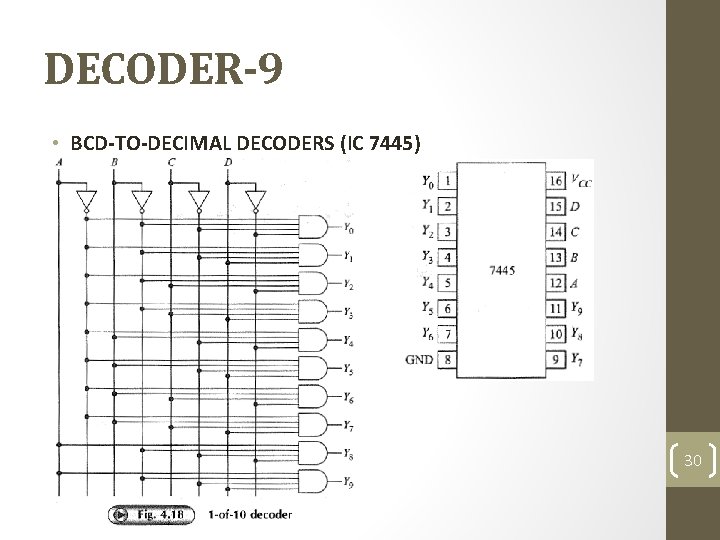
DECODER-9 • BCD-TO-DECIMAL DECODERS (IC 7445) 30
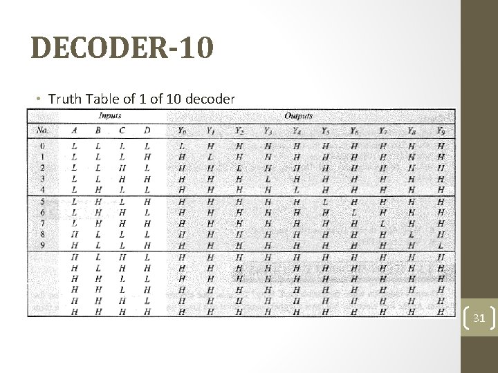
DECODER-10 • Truth Table of 10 decoder 31
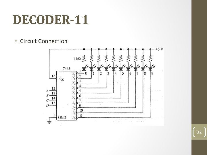
DECODER-11 • Circuit Connection 32
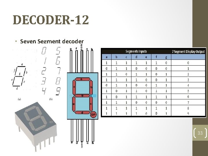
DECODER-12 • Seven Segment decoder 33
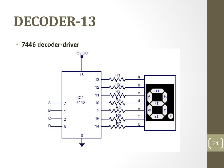
DECODER-13 • 7446 decoder-driver 34
ENCODERS-1 • An encoder converts an active input signal into a coded output signal. • An encoder is a device which converts familiar numbers or characters or symbols into a coded format. It accepts the alphabetic characters and decimal numbers as inputs and produces the outputs as a coded representation of the inputs. • It is a combinational circuit that performs the opposite function of a decoder. • These are mainly used to reduce the number of bits needed to represent given information. 35
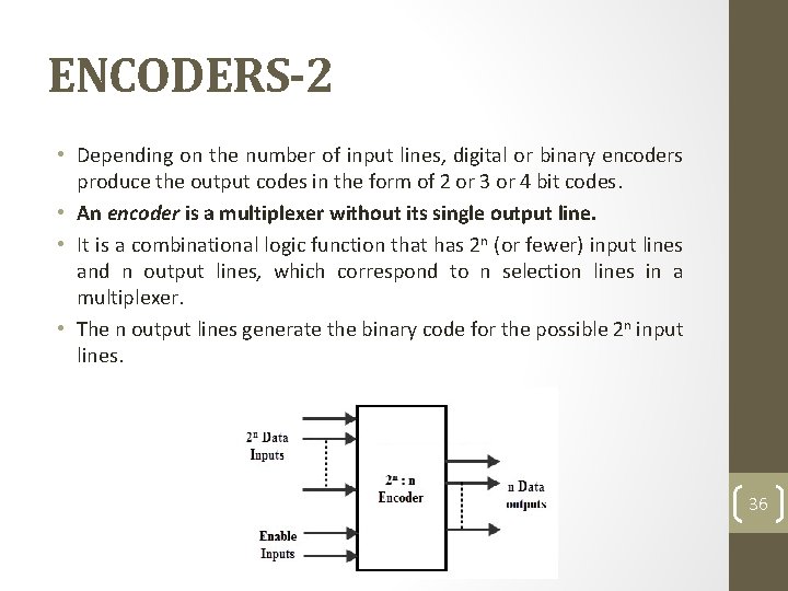
ENCODERS-2 • Depending on the number of input lines, digital or binary encoders produce the output codes in the form of 2 or 3 or 4 bit codes. • An encoder is a multiplexer without its single output line. • It is a combinational logic function that has 2 n (or fewer) input lines and n output lines, which correspond to n selection lines in a multiplexer. • The n output lines generate the binary code for the possible 2 n input lines. 36
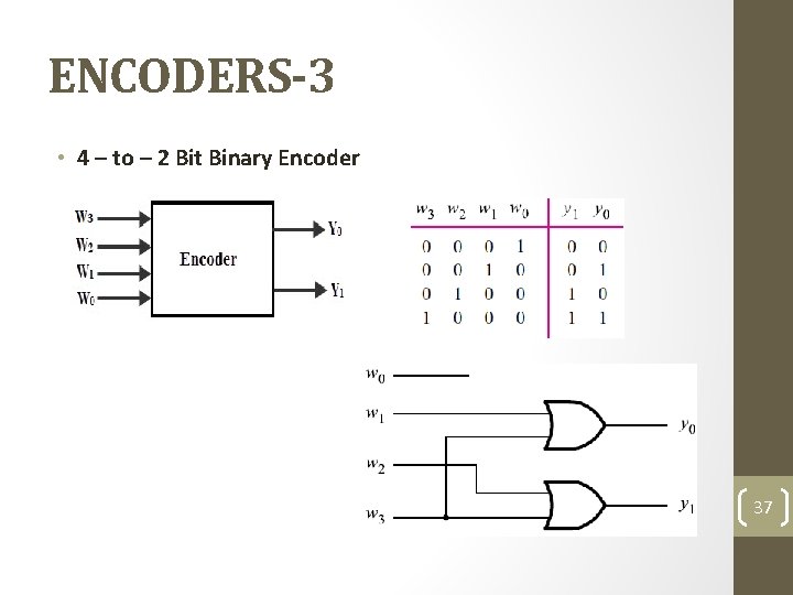
ENCODERS-3 • 4 – to – 2 Bit Binary Encoder 37
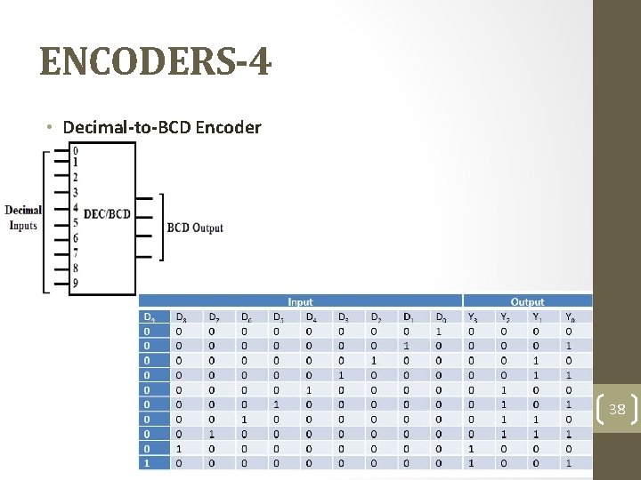
ENCODERS-4 • Decimal-to-BCD Encoder 38
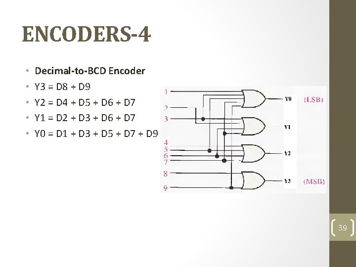
ENCODERS-4 • • • Decimal-to-BCD Encoder Y 3 = D 8 + D 9 Y 2 = D 4 + D 5 + D 6 + D 7 Y 1 = D 2 + D 3 + D 6 + D 7 Y 0 = D 1 + D 3 + D 5 + D 7 + D 9 39
ENCODERS-5 • Priority Encoder • A priority encoder is a practical form of an encoder. The encoders available in IC form are all priority encoders. • In this type of encoder, a priority is assigned to each input so that, when more than one output is simultaneously active, the input with the highest priority is encoded. • Let us assume that the octal-to-binary encoder has an input priority for higher-order digits. • Let us also assume that input lines D 2, D 4 and D 7 are all simultaneously in logic ‘ 1’ state. In that case, only D 7 will be encoded and the output will be 111. 40
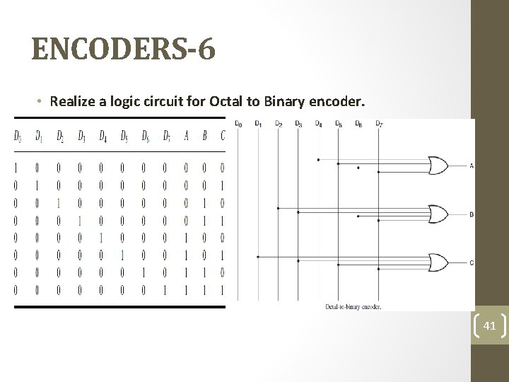
ENCODERS-6 • Realize a logic circuit for Octal to Binary encoder. 41
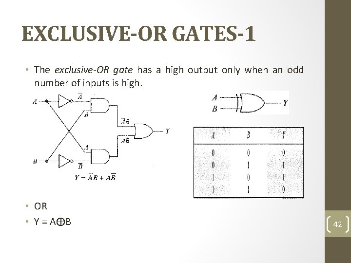
EXCLUSIVE-OR GATES-1 • The exclusive-OR gate has a high output only when an odd number of inputs is high. • OR • Y = A⨁B 42
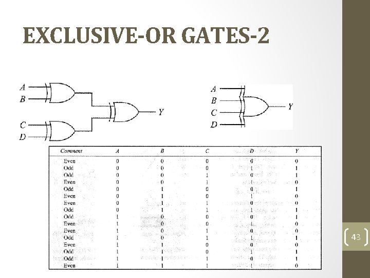
EXCLUSIVE-OR GATES-2 43
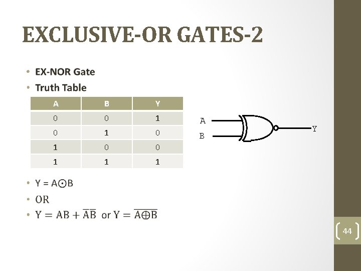
EXCLUSIVE-OR GATES-2 • A B Y 0 0 1 A 0 1 0 B 1 0 0 1 1 1 Y 44
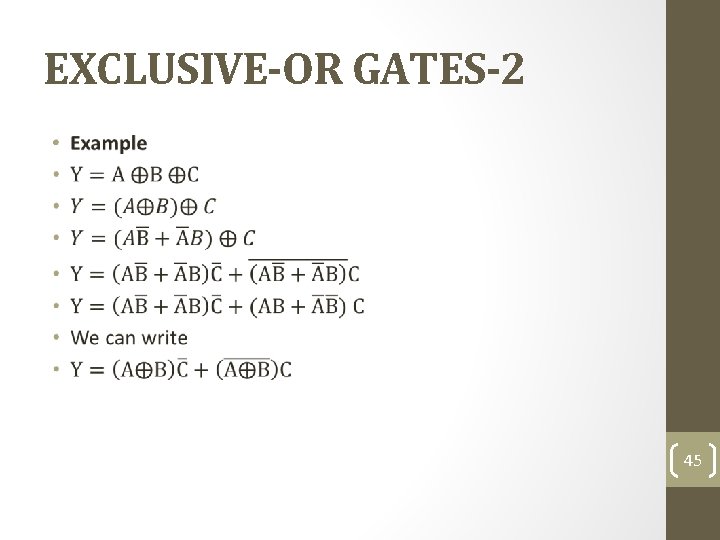
EXCLUSIVE-OR GATES-2 • 45
EXCLUSIVE-OR GATES-3 • PARITY GENERATORS AND CHECKERS • Even parity means an n-bit input has an even number of 1 s. For instance, 110011 has even parity because it contains four 1 s. • Odd parity means an n-bit input has an odd number of 1 s. For example, 110001 has odd parity because it contains three 1 s. 46
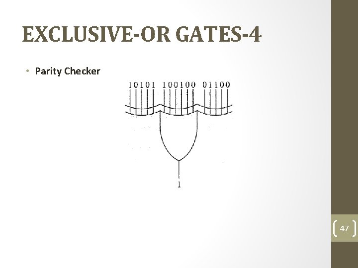
EXCLUSIVE-OR GATES-4 • Parity Checker 47
EXCLUSIVE-OR GATES-5 • Parity Generation • In a computer, a binary number may represent an instruction that tells the computer to add, subtract, and so on; or the binary number may represent data to be processed like a number, letter, etc. In either case, you sometimes will see an extra bit added to the original binary number to produce a new binary number with even or odd parity. 48
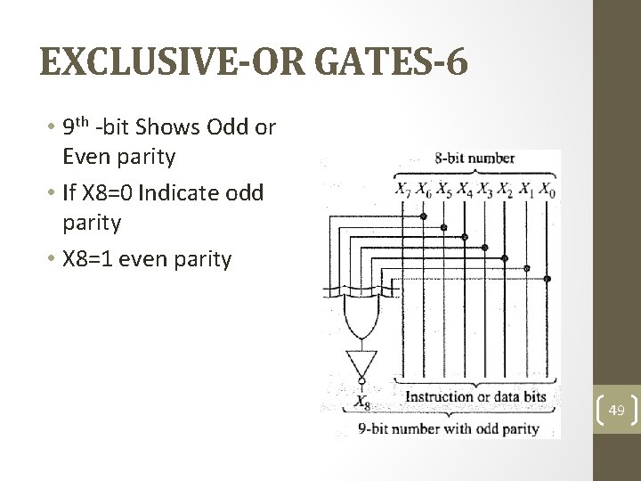
EXCLUSIVE-OR GATES-6 • 9 th -bit Shows Odd or Even parity • If X 8=0 Indicate odd parity • X 8=1 even parity 49
EXCLUSIVE-OR GATES-7 • Application • Practical application of parity generation and checking • Because of transients, noise, and other disturbances, 1 -bit errors sometimes occur when binary data is transmitted over telephone lines or other communication paths. • One way to check for errors is to use an odd-parity generator at the transmitting end an odd-parity checker at the receiving end. If no 1 -bit errors occur in transmission, the received data will have odd parity. • But if one of the transmitted bits is changed by noise or any other disturbance, the received data will have even parity. 50
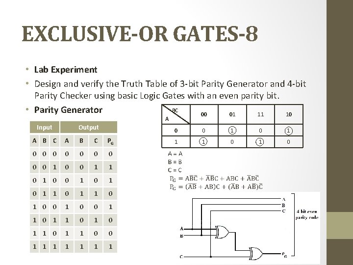
EXCLUSIVE-OR GATES-8 • Lab Experiment • Design and verify the Truth Table of 3 -bit Parity Generator and 4 -bit Parity Checker using basic Logic Gates with an even parity bit. BC • Parity Generator 00 01 11 10 A Input Output A B C PG 0 0 0 0 0 1 1 0 0 1 0 1 0 0 1 1 0 1 1 0 0 1 1 1 0
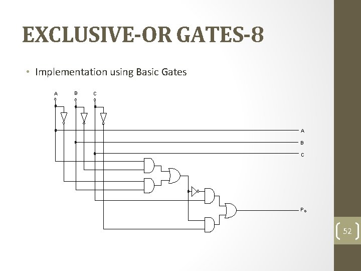
EXCLUSIVE-OR GATES-8 • Implementation using Basic Gates A B C PG 52
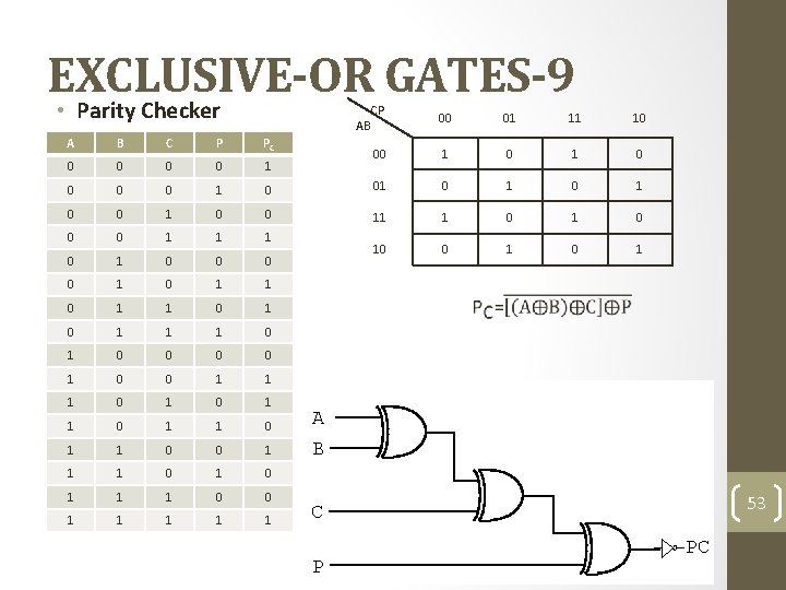
EXCLUSIVE-OR GATES-9 • Parity Checker AB CP 00 01 11 10 00 1 0 A B C P PC 0 0 1 0 01 0 1 0 0 11 1 0 0 0 1 0 1 0 1 1 1 0 0 0 0 1 1 1 0 1 1 0 0 1 1 1 0 0 1 1 1 A B 53 C P PC
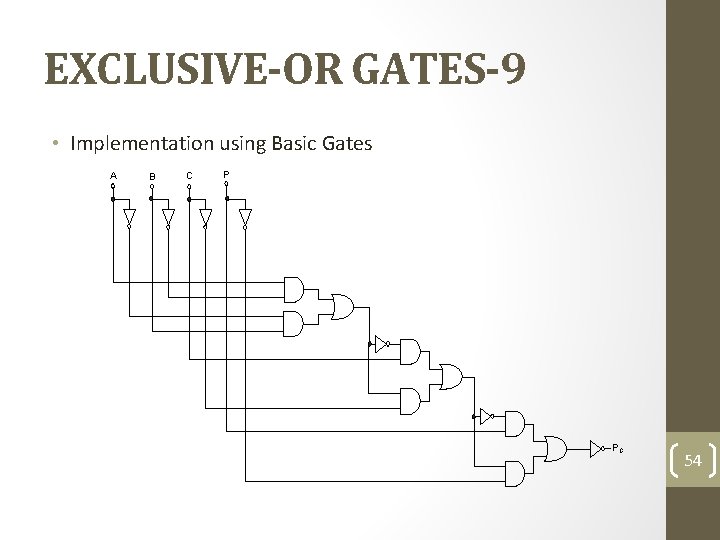
EXCLUSIVE-OR GATES-9 • Implementation using Basic Gates A B C P PC 54
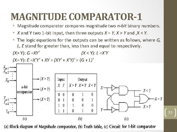
MAGNITUDE COMPARATOR-1 • Magnitude comparator compares magnitude two n-bit binary numbers. • X and Y two 1 -bit Input, then three outputs X = Y, X > Y and , X < Y. • The logic equations for the outputs can be written as follows, where G, L, E stand for greater than, less than and equal to respectively. (X> Y): G =XY' (X < Y): L =X'Y (X= Y): E =X'Y' + XY = (XY' + X'Y)' = (G + L)' 55
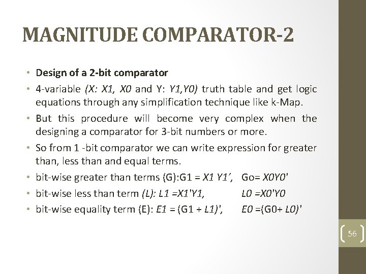
MAGNITUDE COMPARATOR-2 • Design of a 2 -bit comparator • 4 -variable (X: X 1, X 0 and Y: Y 1, Y 0) truth table and get logic equations through any simplification technique like k-Map. • But this procedure will become very complex when the designing a comparator for 3 -bit numbers or more. • So from 1 -bit comparator we can write expression for greater than, less than and equal terms. • bit-wise greater than terms (G): G 1 = X 1 Y 1’, Go= X 0 Y 0' • bit-wise less than term (L): L 1 =X 1'Y 1, L 0 =X 0'Y 0 • bit-wise equality term (E): E 1 = (G 1 + L 1)', E 0 =(G 0+ L 0)' 56
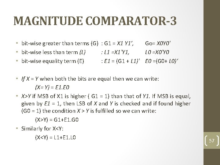
MAGNITUDE COMPARATOR-3 • bit-wise greater than terms (G) : G 1 = X 1 Y 1’, Go= X 0 Y 0' • bit-wise less than term (L) : L 1 =X 1'Y 1, L 0 =X 0'Y 0 • bit-wise equality term (E) : E 1 = (G 1 + L 1)' E 0 =(G 0+ L 0)‘ • If X = Y when both the bits are equal then we can write: (X= Y) = E 1. E 0 • X>Y if MSB of X 1 is higher ( G 1 = 1) than that of Y 1. If MSB is equal, given by E 1 = 1, then LSB of X and Y is checked and if found higher (G 0 = 1) the condition X > Y is fulfilled so we can write: (X>Y) = G 1+E 1. G 0 • Similarly for X<Y: (X<Y) = L 1+E 1. L 0 57
MAGNITUDE COMPARATOR-4 • • • X: Xn- 1 Xn-2. . . X 0 and Y: Yn-1 Yn-2. . Y 0 We can write, (X= Y) = En-1. En-2···Eo (X> Y) = Gn-1 + En-1. Gn-2 +. . . +En-1. En-2··· E 1. G 0 (X < Y) = Ln-1 + En-1. Ln-2 +. . . + En-1. En-2··· E 1. L 0 where Ei, Gi and Li represent for ith bit Xi = Yi, Xi > Yi and Xi < Yi terms respectively. 58
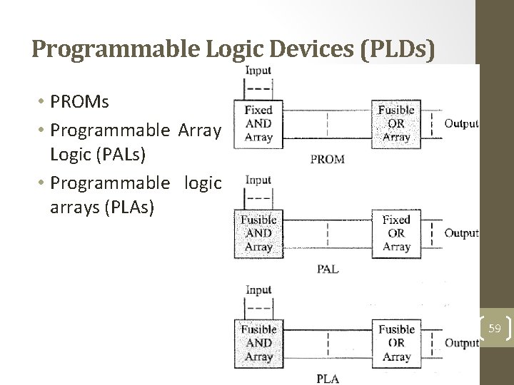
Programmable Logic Devices (PLDs) • PROMs • Programmable Array Logic (PALs) • Programmable logic arrays (PLAs) 59
Programmable Array Logic (PAL)-1 • Programmable array logic (PAL) is a programmable array of logic gates on a single chip. PALs are another design solution, similar to a sum-of-products solution, product-of-sums solution, and multiplexer logic. • A PAL has a programmable AND array and a fixed OR array. 60
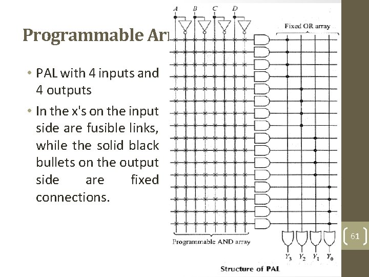
Programmable Array Logic (PAL)-2 • PAL with 4 inputs and 4 outputs • In the x's on the input side are fusible links, while the solid black bullets on the output side are fixed connections. 61
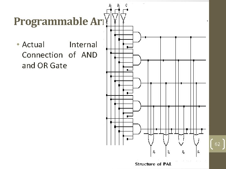
Programmable Array Logic (PAL)-2 • Actual Internal Connection of AND and OR Gate 62
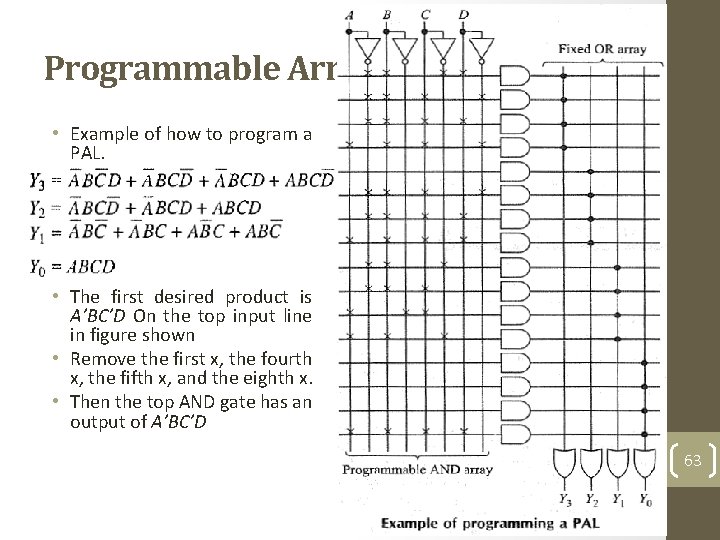
Programmable Array Logic (PAL)-3 • Example of how to program a PAL. • The first desired product is A’BC’D On the top input line in figure shown • Remove the first x, the fourth x, the fifth x, and the eighth x. • Then the top AND gate has an output of A’BC’D 63
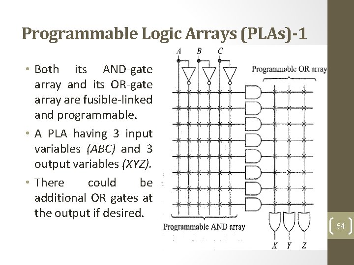
Programmable Logic Arrays (PLAs)-1 • Both its AND-gate array and its OR-gate array are fusible-linked and programmable. • A PLA having 3 input variables (ABC) and 3 output variables (XYZ). • There could be additional OR gates at the output if desired. 64
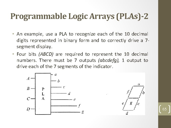
Programmable Logic Arrays (PLAs)-2 • An example, use a PLA to recognize each of the 10 decimal digits represented in binary form and to correctly drive a 7 segment display. • Four bits (ABCD) are required to represent the 10 decimal numbers. There must be 7 outputs (abcdefg), 1 output to drive each of the 7 segments of the indicator. 65
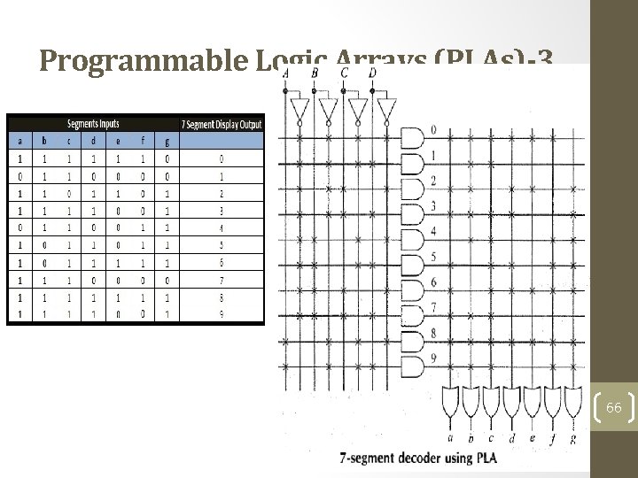
Programmable Logic Arrays (PLAs)-3 66
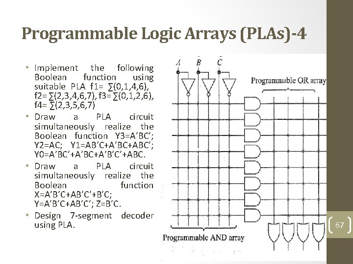
Programmable Logic Arrays (PLAs)-4 • Implement the following Boolean function using suitable PLA f 1= ∑(0, 1, 4, 6), f 2= ∑(2, 3, 4, 6, 7), f 3= ∑(0, 1, 2, 6), f 4= ∑(2, 3, 5, 6, 7) • Draw a PLA circuit simultaneously realize the Boolean function Y 3=A’BC’; Y 2=AC; Y 1=AB’C+A’BC+ABC’; Y 0=A’BC’+A’BC+A’B’C’+ABC. • Draw a PLA circuit simultaneously realize the Boolean function X=A’B’C+AB’C’+B’C; Y=A’B’C+AB’C’; Z=B’C. • Design 7 -segment decoder using PLA. 67
HDL IMPLEMENTATION OF DATA PROCESSING CIRCUITS-1 • The data flow model provides a different use of keyword assign in the form of assign X = S ? A : B; • If, S = 1, X = A and if S = 0, X = B. 68
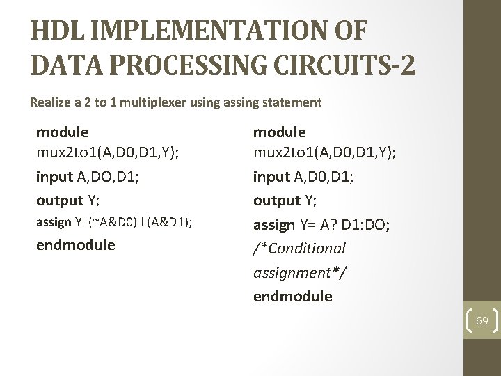
HDL IMPLEMENTATION OF DATA PROCESSING CIRCUITS-2 Realize a 2 to 1 multiplexer using assing statement module mux 2 to 1(A, D 0, D 1, Y); input A, DO, D 1; output Y; assign Y=(~A&D 0) I (A&D 1); endmodule mux 2 to 1(A, D 0, D 1, Y); input A, D 0, D 1; output Y; assign Y= A? D 1: DO; /*Conditional assignment*/ endmodule 69
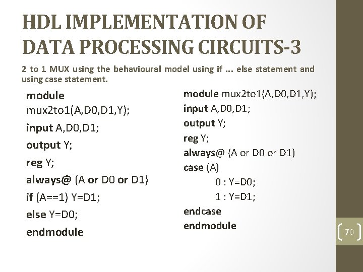
HDL IMPLEMENTATION OF DATA PROCESSING CIRCUITS-3 2 to 1 MUX using the behavioural model using if. . . else statement and using case statement. module mux 2 to 1(A, D 0, D 1, Y); input A, D 0, D 1; output Y; reg Y; always@ (A or D 0 or D 1) if (A==1) Y=D 1; else Y=D 0; endmodule mux 2 to 1(A, D 0, D 1, Y); input A, D 0, D 1; output Y; reg Y; always@ (A or D 0 or D 1) case (A) 0 : Y=D 0; 1 : Y=D 1; endcase endmodule 70
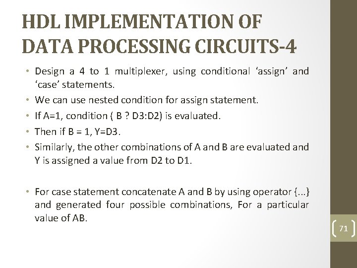
HDL IMPLEMENTATION OF DATA PROCESSING CIRCUITS-4 • Design a 4 to 1 multiplexer, using conditional ‘assign’ and ‘case’ statements. • We can use nested condition for assign statement. • If A=1, condition ( B ? D 3: D 2) is evaluated. • Then if B = 1, Y=D 3. • Similarly, the other combinations of A and B are evaluated and Y is assigned a value from D 2 to D 1. • For case statement concatenate A and B by using operator {. . . } and generated four possible combinations, For a particular value of AB. 71
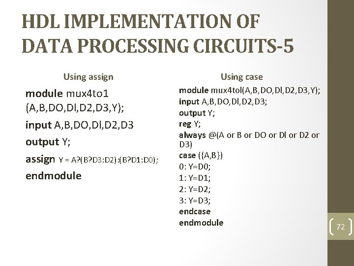
HDL IMPLEMENTATION OF DATA PROCESSING CIRCUITS-5 Using assign module mux 4 to 1 (A, B, DO, Dl, D 2, D 3, Y); input A, B, DO, Dl, D 2, D 3 output Y; assign Y = A? (B? D 3: D 2): (B? D 1: D 0); endmodule Using case module mux 4 tol(A, B, DO, Dl, D 2, D 3, Y); input A, B, DO, Dl, D 2, D 3; output Y; reg Y; always @(A or B or DO or Dl or D 2 or D 3) case ({A, B}) 0: Y=D 0; 1: Y=D 1; 2: Y=D 2; 3: Y=D 3; endcase endmodule 72
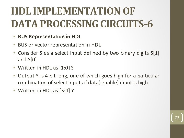
HDL IMPLEMENTATION OF DATA PROCESSING CIRCUITS-6 • BUS Representation in HDL • BUS or vector representation in HDL • Consider S as a select input defined by two binary digits S[1] and S[0] • Written in HDL as [1: 0] S • Output Y is 4 bit long, one of which goes high for a particular combination of select inputs if data( enable) input is high. • Written in HDL as [3: 0] Y 73
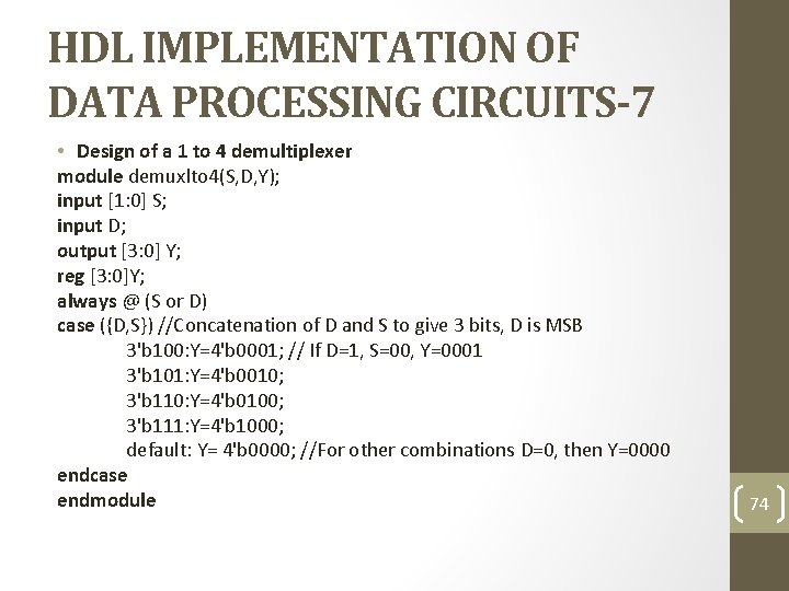
HDL IMPLEMENTATION OF DATA PROCESSING CIRCUITS-7 • Design of a 1 to 4 demultiplexer module demuxlto 4(S, D, Y); input [1: 0] S; input D; output [3: 0] Y; reg [3: 0]Y; always @ (S or D) case ({D, S}) //Concatenation of D and S to give 3 bits, D is MSB 3'b 100: Y=4'b 0001; // If D=1, S=00, Y=0001 3'b 101: Y=4'b 0010; 3'b 110: Y=4'b 0100; 3'b 111: Y=4'b 1000; default: Y= 4'b 0000; //For other combinations D=0, then Y=0000 endcase endmodule 74
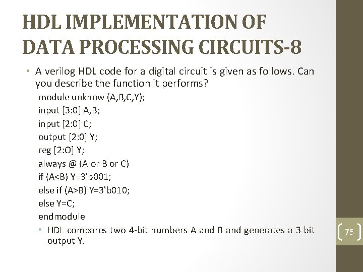
HDL IMPLEMENTATION OF DATA PROCESSING CIRCUITS-8 • A verilog HDL code for a digital circuit is given as follows. Can you describe the function it performs? module unknow (A, B, C, Y); input [3: 0] A, B; input [2: 0] C; output [2: 0] Y; reg [2: O] Y; always @ (A or B or C) if (A<B) Y=3'b 001; else if (A>B) Y=3'b 010; else Y=C; endmodule • HDL compares two 4 -bit numbers A and B and generates a 3 bit output Y. 75
Arithmetic Building Blocks-1 • Objective • Describe the half-adder, full-adder, and adder-subtractor. • Describe how an Arithmetic Logic Unit can be operated. 76
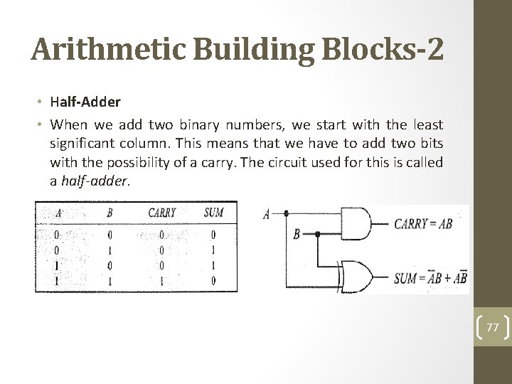
Arithmetic Building Blocks-2 • Half-Adder • When we add two binary numbers, we start with the least significant column. This means that we have to add two bits with the possibility of a carry. The circuit used for this is called a half-adder. 77
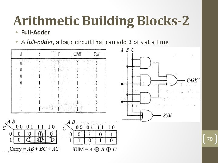
Arithmetic Building Blocks-2 • Full-Adder • A full-adder, a logic circuit that can add 3 bits at a time 78
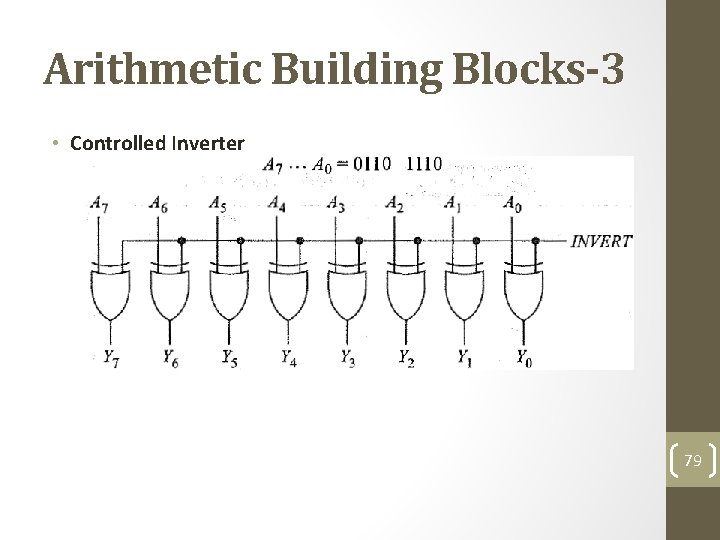
Arithmetic Building Blocks-3 • Controlled Inverter 79
Arithmetic Building Blocks-4 • A Low INVERT produces • Y 1···Yo=0110 1110 • But a High INVERT results in • Y 1. . . Yo= 1001 0001 • During a subtraction, we first need to take the 2's complement of the subtrahend. Then we can add the complemented subtrahend to obtain the answer. • With a controlled inverter, we can produce the 1's complement. There is an easy way to get the 2 's complement. 80
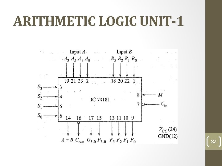
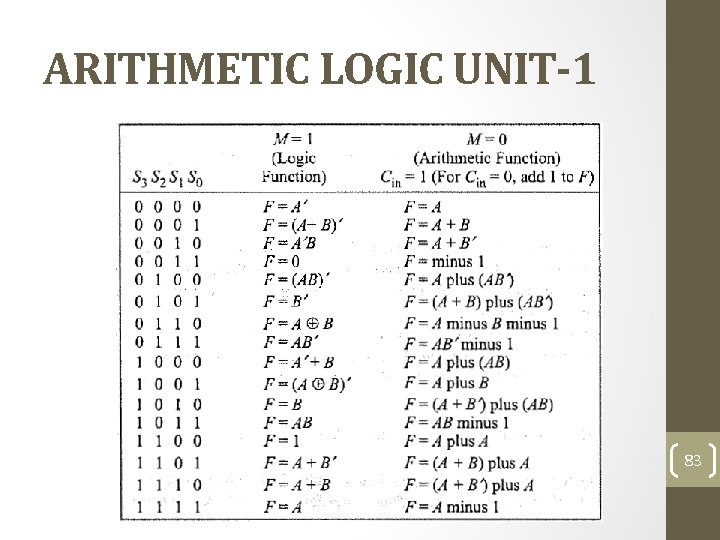
ARITHMETIC LOGIC UNIT-1 • ALU is an integral part of central processing unit or CPU of a computer. It comes in various forms with wide range of functionality. • Like normal addition, subtraction, increment, decrement operations. • As logic unit it performs usual AND, OR, NOT, EX-OR and many other complex logic functions. • It also comes with PRESET and CLEAR options, invoking which all the function outputs are made 1 and 0 respectively. • Normally, a mode selector input (M) decides whether ALU performs a logic operation or an arithmetic operation. 81
ARITHMETIC LOGIC UNIT-1 82
ARITHMETIC LOGIC UNIT-1 83

Flip-Flops 84
Introduction • The outputs of the digital circuits are dependent entirely on their inputs. • However, there are requirements for a digital device or circuit whose output will remain unchanged, once set, even if there is a change in input level(s). Such a device could be used to store a binary number called Flip-Flop. • Flip-flops are used in the construction of registers and counters, and in numerous other applications. • In a sequential logic circuit flip-flops serve as key memory elements. • Analysis of such circuits are done through truth tables or characteristic equations of flip-flops. The analysis result is normally presented through state table or state transition diagram and also through timing diagram. 85
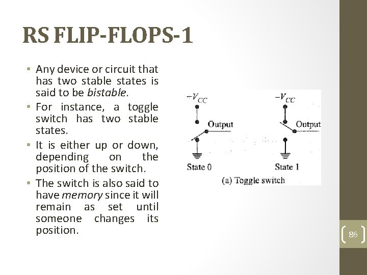
RS FLIP-FLOPS-1 • Any device or circuit that has two stable states is said to be bistable. • For instance, a toggle switch has two stable states. • It is either up or down, depending on the position of the switch. • The switch is also said to have memory since it will remain as set until someone changes its position. 86
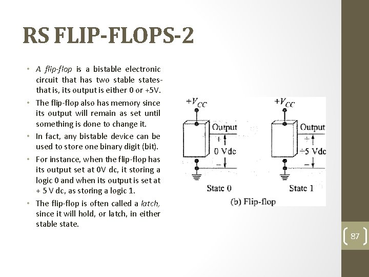
RS FLIP-FLOPS-2 • A flip-flop is a bistable electronic circuit that has two stable statesthat is, its output is either 0 or +5 V. • The flip-flop also has memory since its output will remain as set until something is done to change it. • In fact, any bistable device can be used to store one binary digit (bit). • For instance, when the flip-flop has its output set at 0 V dc, it storing a logic 0 and when its output is set at + 5 V dc, as storing a logic 1. • The flip-flop is often called a latch, since it will hold, or latch, in either stable state. 87
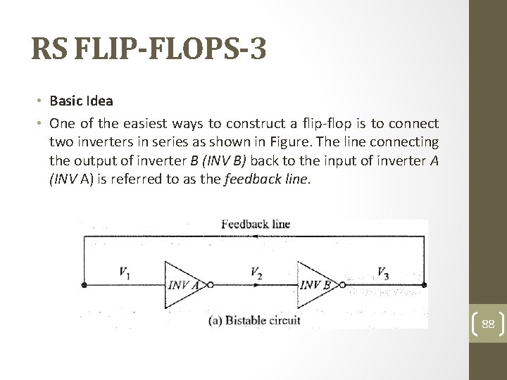
RS FLIP-FLOPS-3 • Basic Idea • One of the easiest ways to construct a flip-flop is to connect two inverters in series as shown in Figure. The line connecting the output of inverter B (INV B) back to the input of inverter A (INV A) is referred to as the feedback line. 88
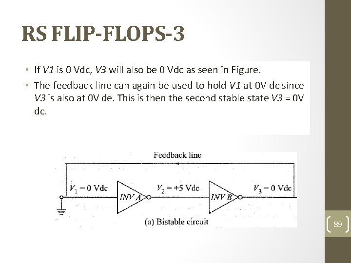
RS FLIP-FLOPS-3 • Basic If V 1 is. Idea 0 Vdc, V 3 will also be 0 Vdc as seen in Figure. • The One feedback of the easiest line can ways again to construct be used toa hold flip-flop V 1 at is 0 V to dc connect since twoisinverters V 3 also at 0 Vinde. series Thisas is shown the in second Figure. stable The line state connecting V 3 = 0 V the output of inverter B (INV B) back to the input of inverter A dc. (INV A) is referred to as the feedback line. 89
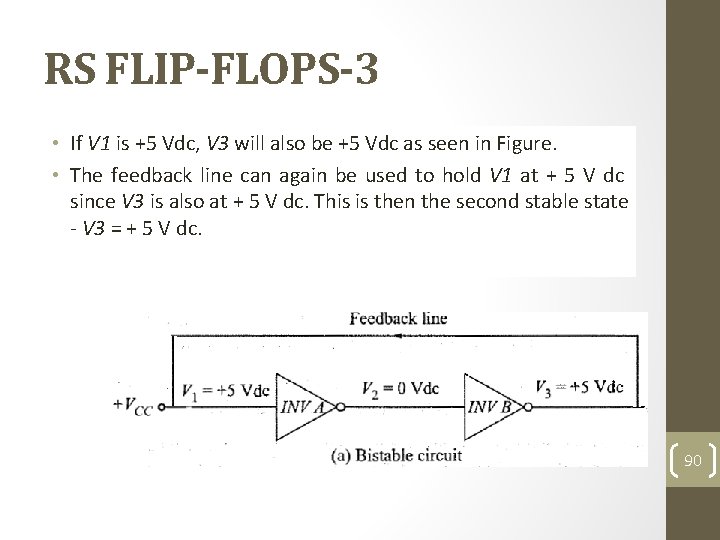
RS FLIP-FLOPS-3 • If Basic V 1 is. Idea +5 0 Vdc, V 3 willalsobe be 0+5 Vdc as as seen in Figure. • The One feedback of the easiest line can ways again to construct be beusedtoatohold flip-flop hold V 1 V 1 at isat 0 V to+dc connect 5 since V dc twoisinverters V 3 since also V 3 isatalso 0 Vinde. at series +This 5 Vas is dc. shown then Thisthe isinthen second Figure. thestable The second line state stable connecting V 3 state = 0 V the -dc. V 3 output = + 5 Vof dc. inverter B (INV B) back to the input of inverter A (INV A) is referred to as the feedback line. 90
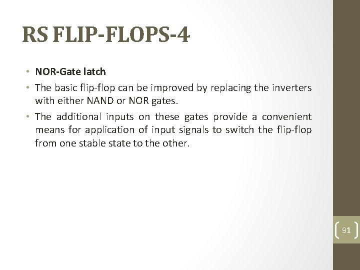
RS FLIP-FLOPS-4 • NOR-Gate latch • The basic flip-flop can be improved by replacing the inverters with either NAND or NOR gates. • The additional inputs on these gates provide a convenient means for application of input signals to switch the flip-flop from one stable state to the other. 91
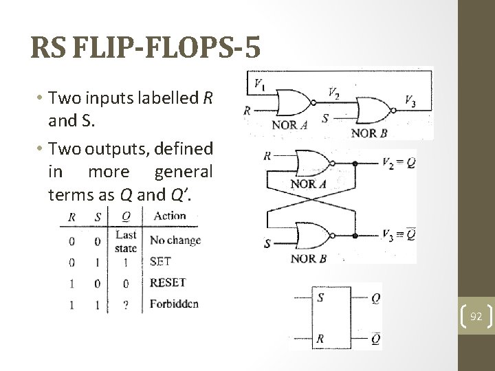
RS FLIP-FLOPS-5 • Two inputs labelled R and S. • Two outputs, defined in more general terms as Q and Q’. 92
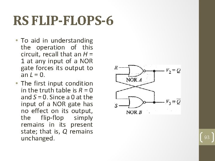
RS FLIP-FLOPS-6 • To aid in understanding the operation of this circuit, recall that an H = 1 at any input of a NOR gate forces its output to an L = 0. • The first input condition in the truth table is R = 0 and S = 0. Since a 0 at the input of a NOR gate has no effect on its output, the flip-flop simply remains in its present state; that is, Q remains unchanged. 93
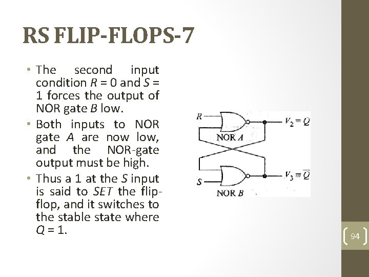
RS FLIP-FLOPS-7 • The second input condition R = 0 and S = 1 forces the output of NOR gate B low. • Both inputs to NOR gate A are now low, and the NOR-gate output must be high. • Thus a 1 at the S input is said to SET the flipflop, and it switches to the stable state where Q = 1. 94
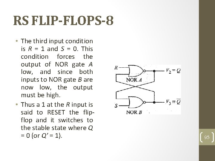
RS FLIP-FLOPS-8 • The third input condition is R = 1 and S = 0. This condition forces the output of NOR gate A low, and since both inputs to NOR gate B are now low, the output must be high. • Thus a 1 at the R input is said to RESET the flipflop and it switches to the stable state where Q = 0 (or Q’ = 1). 95
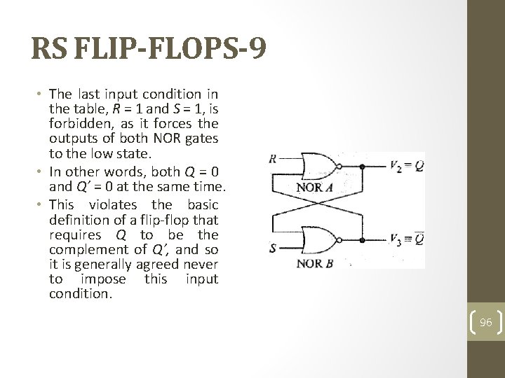
RS FLIP-FLOPS-9 • The last input condition in the table, R = 1 and S = 1, is forbidden, as it forces the outputs of both NOR gates to the low state. • In other words, both Q = 0 and Q’ = 0 at the same time. • This violates the basic definition of a flip-flop that requires Q to be the complement of Q’, and so it is generally agreed never to impose this input condition. 96
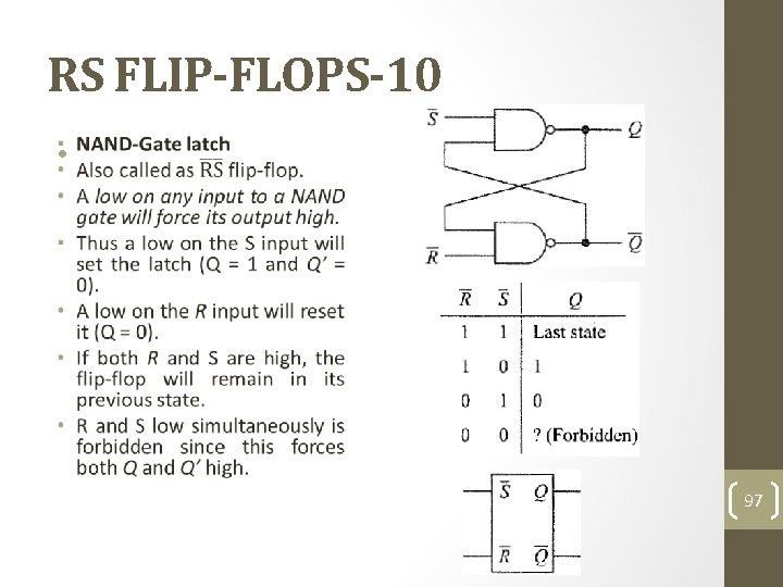
RS FLIP-FLOPS-10 • 97
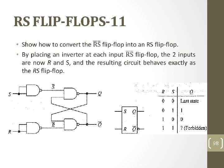
RS FLIP-FLOPS-11 • 98
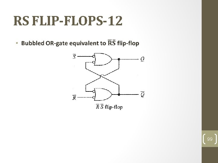
RS FLIP-FLOPS-12 • 99
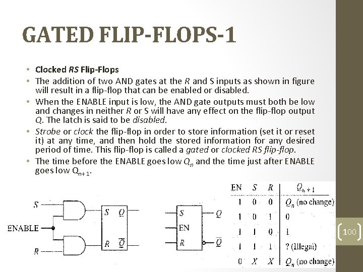
GATED FLIP-FLOPS-1 • Clocked RS Flip-Flops • The addition of two AND gates at the R and S inputs as shown in figure will result in a flip-flop that can be enabled or disabled. • When the ENABLE input is low, the AND gate outputs must both be low and changes in neither R or S will have any effect on the flip-flop output Q. The latch is said to be disabled. • Strobe or clock the flip-flop in order to store information (set it or reset it) at any time, and then hold the stored information for any desired period of time. This flip-flop is called a gated or clocked RS flip-flop. • The time before the ENABLE goes low Qn and the time just after ENABLE goes low Qn+ 1. 100
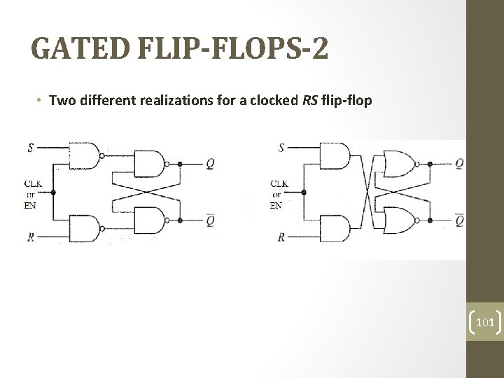
GATED FLIP-FLOPS-2 • Two different realizations for a clocked RS flip-flop 101
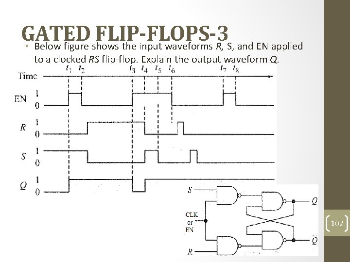
GATED FLIP-FLOPS-3 • Below figure shows the input waveforms R, S, and EN applied to a clocked RS flip-flop. Explain the output waveform Q. 102
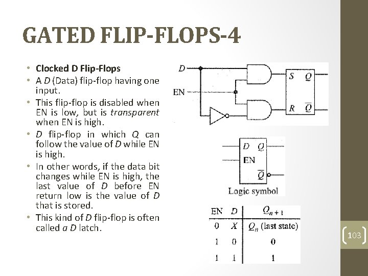
GATED FLIP-FLOPS-4 • Clocked D Flip-Flops • A D (Data) flip-flop having one input. • This flip-flop is disabled when EN is low, but is transparent when EN is high. • D flip-flop in which Q can follow the value of D while EN is high. • In other words, if the data bit changes while EN is high, the last value of D before EN return low is the value of D that is stored. • This kind of D flip-flop is often called a D latch. 103
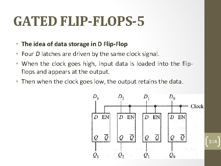
GATED FLIP-FLOPS-5 • The idea of data storage in D Flip-Flop • Four D latches are driven by the same clock signal. • When the clock goes high, input data is loaded into the flipflops and appears at the output. • Then when the clock goes low, the output retains the data. 104
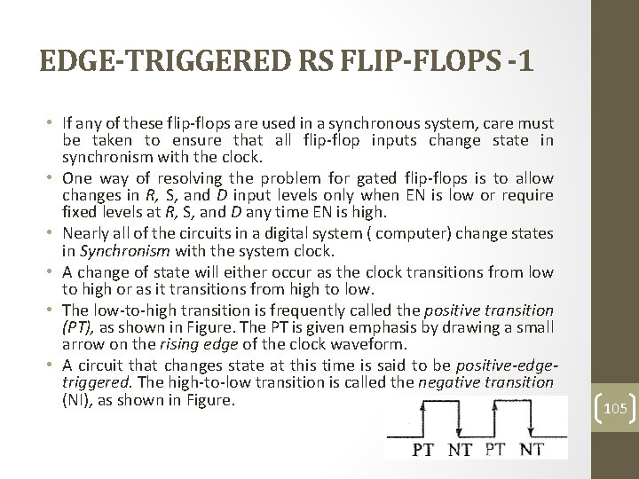
EDGE-TRIGGERED RS FLIP-FLOPS -1 • If any of these flip-flops are used in a synchronous system, care must be taken to ensure that all flip-flop inputs change state in synchronism with the clock. • One way of resolving the problem for gated flip-flops is to allow changes in R, S, and D input levels only when EN is low or require fixed levels at R, S, and D any time EN is high. • Nearly all of the circuits in a digital system ( computer) change states in Synchronism with the system clock. • A change of state will either occur as the clock transitions from low to high or as it transitions from high to low. • The low-to-high transition is frequently called the positive transition (PT), as shown in Figure. The PT is given emphasis by drawing a small arrow on the rising edge of the clock waveform. • A circuit that changes state at this time is said to be positive-edgetriggered. The high-to-low transition is called the negative transition (NI), as shown in Figure. 105
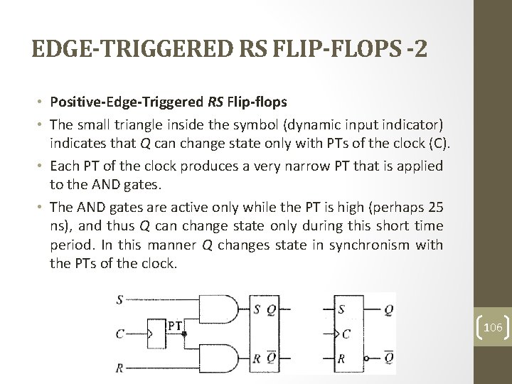
EDGE-TRIGGERED RS FLIP-FLOPS -2 • Positive-Edge-Triggered RS Flip-flops • The small triangle inside the symbol (dynamic input indicator) indicates that Q can change state only with PTs of the clock (C). • Each PT of the clock produces a very narrow PT that is applied to the AND gates. • The AND gates are active only while the PT is high (perhaps 25 ns), and thus Q can change state only during this short time period. In this manner Q changes state in synchronism with the PTs of the clock. 106
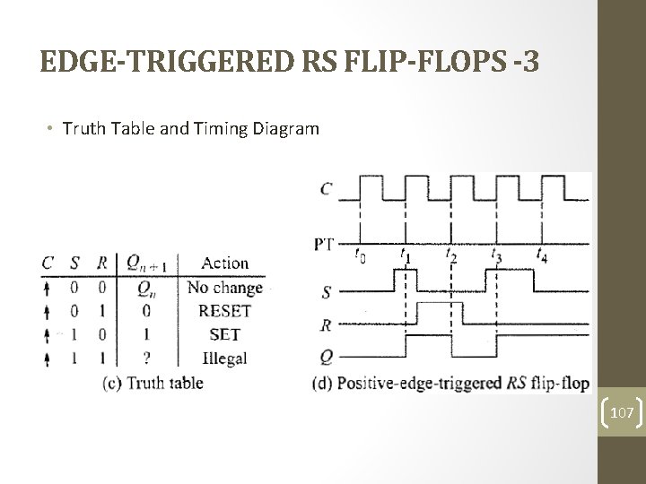
EDGE-TRIGGERED RS FLIP-FLOPS -3 • Truth Table and Timing Diagram 107
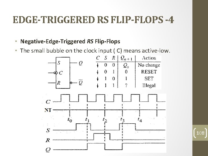
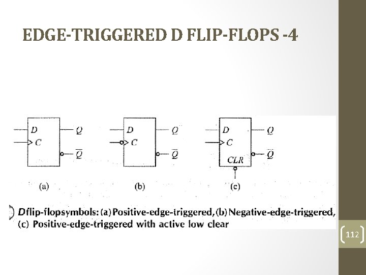
EDGE-TRIGGERED RS FLIP-FLOPS -4 • Negative-Edge-Triggered RS Flip-Flops • The small bubble on the clock input ( C) means active-low. 108
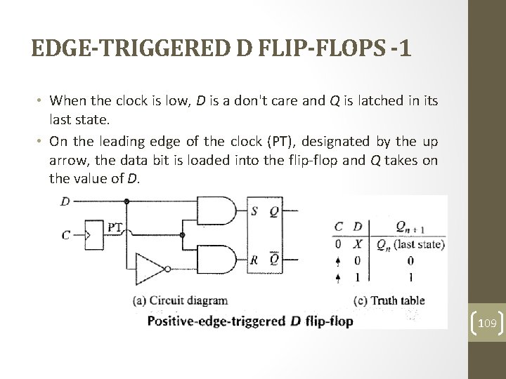
EDGE-TRIGGERED D FLIP-FLOPS -1 • When the clock is low, D is a don't care and Q is latched in its last state. • On the leading edge of the clock (PT), designated by the up arrow, the data bit is loaded into the flip-flop and Q takes on the value of D. 109
EDGE-TRIGGERED D FLIP-FLOPS -2 • To get some computers started, an operator has to push a RESET button. This sends a CLEAR or PRESET signal to all flipflops. Also, it's necessary in some digital systems to preset (synonymous with set) certain flip-flops. 110
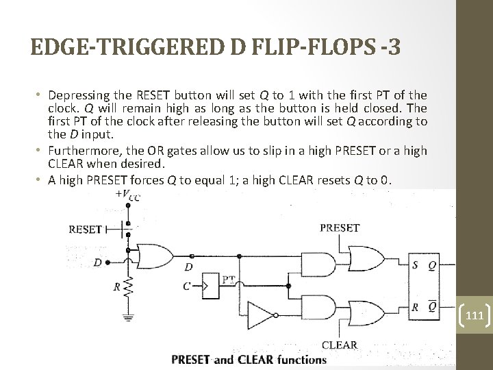
EDGE-TRIGGERED D FLIP-FLOPS -3 • Depressing the RESET button will set Q to 1 with the first PT of the clock. Q will remain high as long as the button is held closed. The first PT of the clock after releasing the button will set Q according to the D input. • Furthermore, the OR gates allow us to slip in a high PRESET or a high CLEAR when desired. • A high PRESET forces Q to equal 1; a high CLEAR resets Q to 0. 111
EDGE-TRIGGERED D FLIP-FLOPS -4 112
EDGE-TRIGGERED JK FLIP-FLOPS -1 • 113
EDGE-TRIGGERED JK FLIP-FLOPS -2 • 114
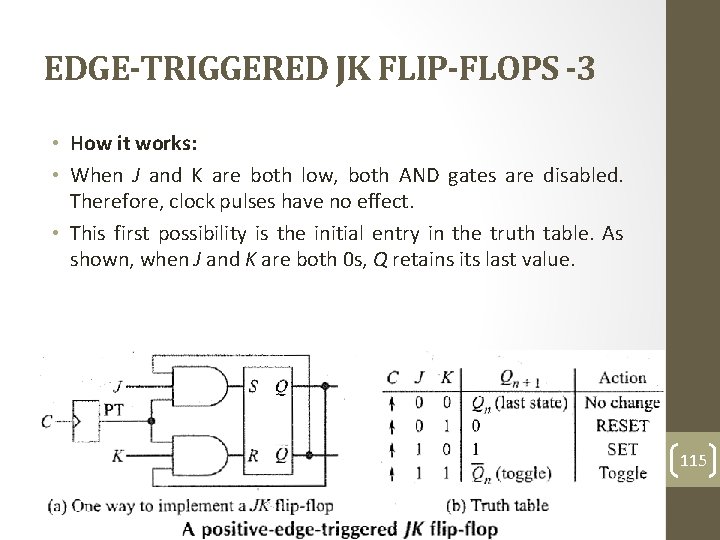
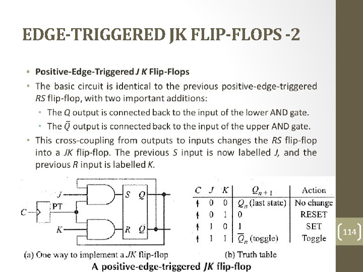
EDGE-TRIGGERED JK FLIP-FLOPS -3 • How it works: • When J and K are both low, both AND gates are disabled. Therefore, clock pulses have no effect. • This first possibility is the initial entry in the truth table. As shown, when J and K are both 0 s, Q retains its last value. 115
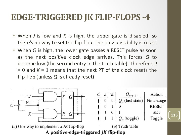
EDGE-TRIGGERED JK FLIP-FLOPS -4 • When J is low and K is high, the upper gate is disabled, so there's no way to set the flip-flop. The only possibility is reset. • When Q is high, the lower gate passes a RESET pulse as soon as the next positive clock edge arrives. This forces Q to become low (the second entry in the truth table). Therefore, J = 0 and K = 1 means that the next PT of the clock resets the flip-flop (unless Q is already reset). 116
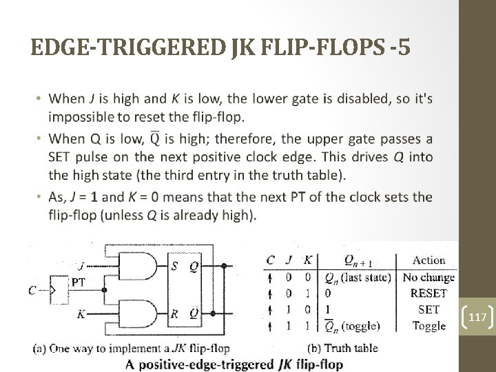
EDGE-TRIGGERED JK FLIP-FLOPS -5 • 117
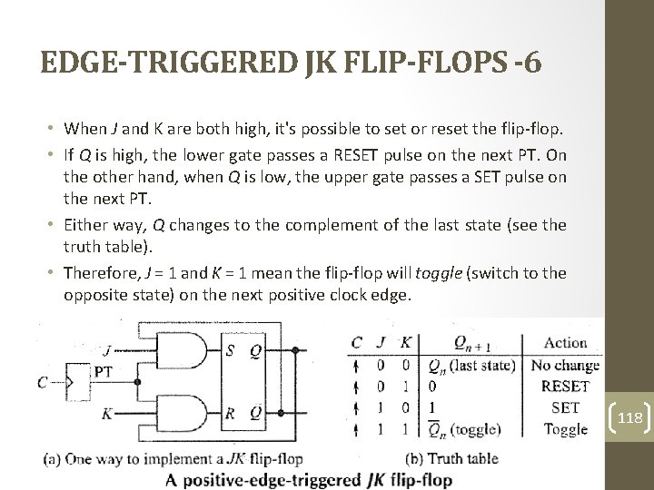
EDGE-TRIGGERED JK FLIP-FLOPS -6 • When J and K are both high, it's possible to set or reset the flip-flop. • If Q is high, the lower gate passes a RESET pulse on the next PT. On the other hand, when Q is low, the upper gate passes a SET pulse on the next PT. • Either way, Q changes to the complement of the last state (see the truth table). • Therefore, J = 1 and K = 1 mean the flip-flop will toggle (switch to the opposite state) on the next positive clock edge. 118
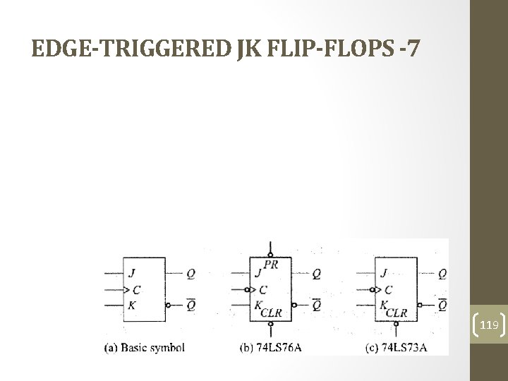
EDGE-TRIGGERED JK FLIP-FLOPS -7 119
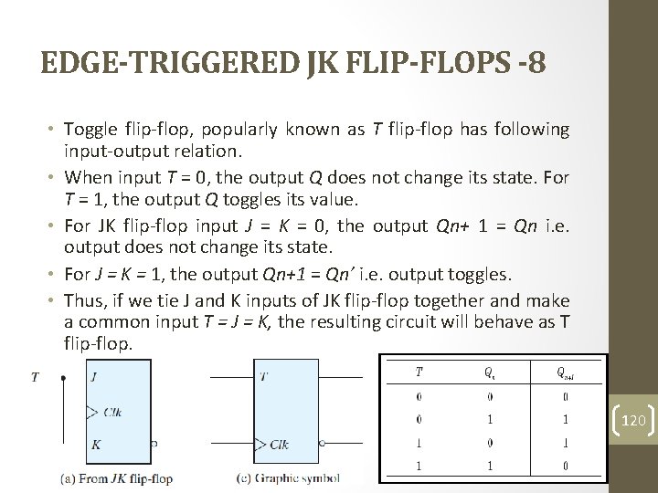
EDGE-TRIGGERED JK FLIP-FLOPS -8 • Toggle flip-flop, popularly known as T flip-flop has following input-output relation. • When input T = 0, the output Q does not change its state. For T = 1, the output Q toggles its value. • For JK flip-flop input J = K = 0, the output Qn+ 1 = Qn i. e. output does not change its state. • For J = K = 1, the output Qn+1 = Qn’ i. e. output toggles. • Thus, if we tie J and K inputs of JK flip-flop together and make a common input T = J = K, the resulting circuit will behave as T flip-flop. 120
- Slides: 120