MODULE I Transistor Types BJT JFET and MOSFET
MODULE I Transistor Types: BJT, JFET, and MOSFET Bipolar Junction Transistor (BJT) – NPN and PNP • Junction Field Effect Transistor (JFET) – N-channel and P-channel • Metal Oxide Semiconductor FET (MOSFET) – Depletion type (n- and p-channel) and enhancement type (n- and p-channel)
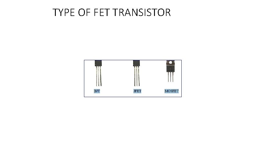
TYPE OF FET TRANSISTOR
BJT Types • NPN and PNP. – NPN: a small input current and a positive voltage applied @ its base (with VB>VE) • allows a large current to flow from collector to emitter. – PNP: a small output current and a negative voltage @ its base (with VB<VE) allows a • much larger current to flow from emitter to collector.
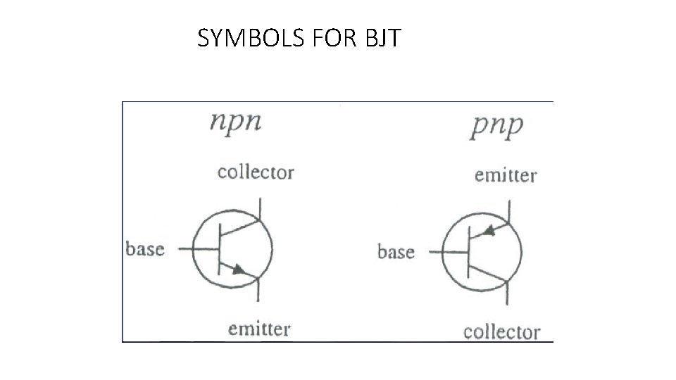
SYMBOLS FOR BJT
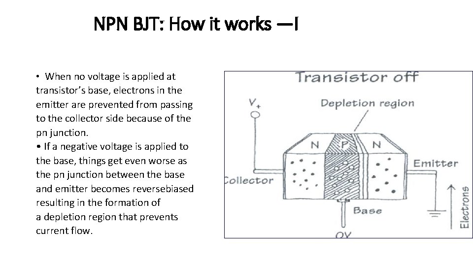
NPN BJT: How it works —I • When no voltage is applied at transistor’s base, electrons in the emitter are prevented from passing to the collector side because of the pn junction. • If a negative voltage is applied to the base, things get even worse as the pn junction between the base and emitter becomes reversebiased resulting in the formation of a depletion region that prevents current flow.
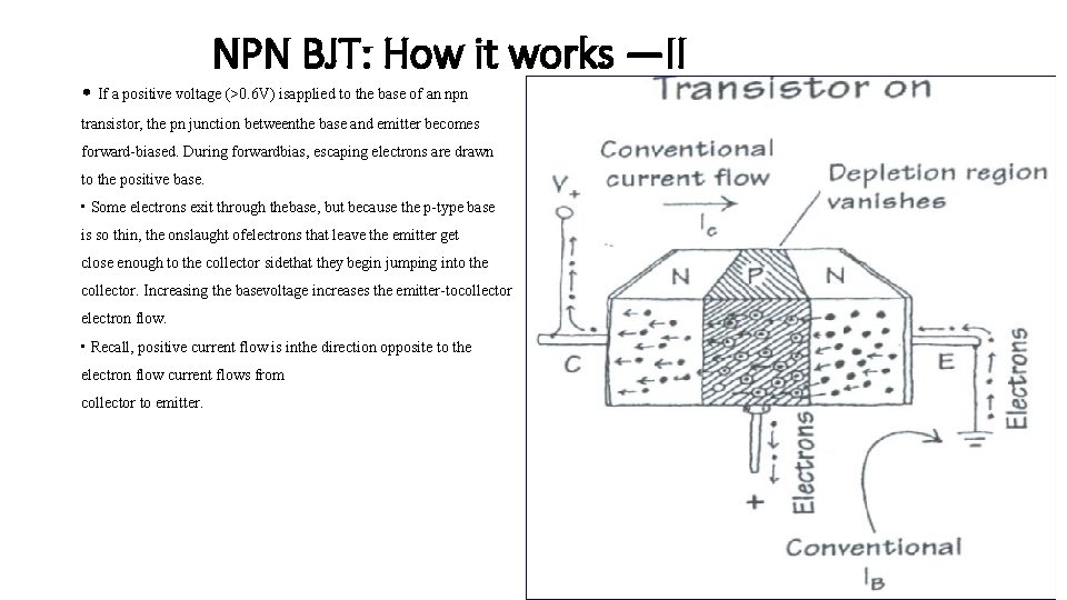
NPN BJT: How it works —II • If a positive voltage (>0. 6 V) isapplied to the base of an npn transistor, the pn junction betweenthe base and emitter becomes forward-biased. During forwardbias, escaping electrons are drawn to the positive base. • Some electrons exit through thebase, but because the p-type base is so thin, the onslaught ofelectrons that leave the emitter get close enough to the collector sidethat they begin jumping into the collector. Increasing the basevoltage increases the emitter-tocollector electron flow. • Recall, positive current flow is inthe direction opposite to the electron flow current flows from collector to emitter.
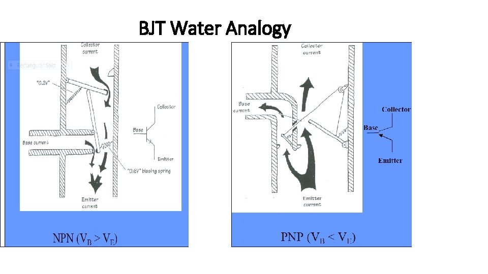
BJT Water Analogy
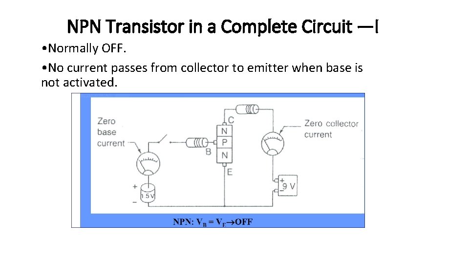
NPN Transistor in a Complete Circuit —I • Normally OFF. • No current passes from collector to emitter when base is not activated.
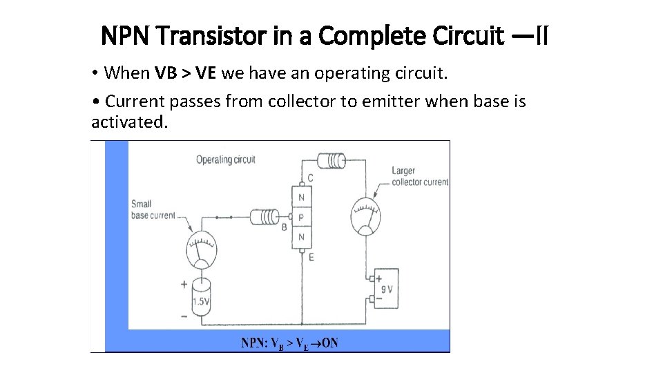
NPN Transistor in a Complete Circuit —II • When VB > VE we have an operating circuit. • Current passes from collector to emitter when base is activated.
MODULE II : JFET • Junction field effect transistors like BJTs are three lead semiconductor devices. • JFETs are used as: – electrically controlled switches, – current amplifiers, and – voltage-controlled resistors. • Unlike BJTs, JFETs do not require a bias current and are controlled by using only a voltage. • JFETs are normally on when VG - VS = 0. • When VG - VS ≠ 0, then JFETs become resistive to current flow through the drain-source pair �“JFETs are depletion devices. ”
JFET Types • Two types of JFETs: – n-channel and p-channel. • In n-channel JFET, a –ve voltage applied @ its gate (with VG < VS) reduces current flow from drain to source. It operates with VD > VS. • In p-channel JFET, a +ve voltage applied @ its gate (with VG > VS) reduces current flow from source to drain. It operates with VS > VD. • JFETs have very high input impedance and draw little or no input current – if there is any circuit/component connected to the gate of a JFET, no current is drawn away from or sunk into this circuit.
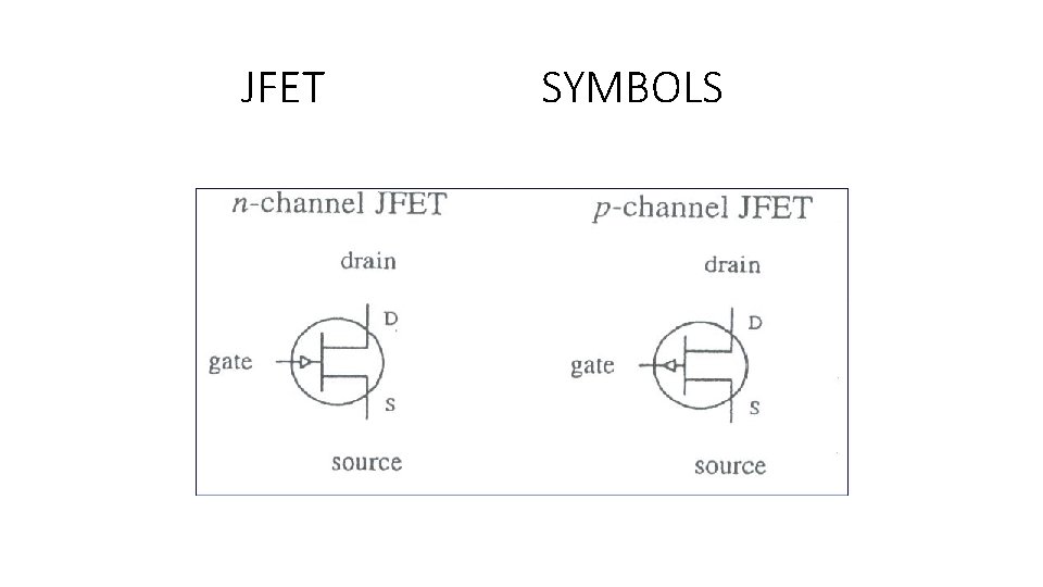
JFET SYMBOLS
MOSFET • Metal oxide semiconductor FET. • Similar to JFET. • A metal oxide insulator is placed @ the gate to obtain a high input impedance @ the gate – gate input impedance approx. 1014Ω. • Use of insulator as described above yields a low gate-to-channel capacitance. – If too much static electricity builds up on the gate, then the MOSFET may be damaged.
- Slides: 13