Module 27 Solar PV Module Technologies Module 1
- Slides: 15

Module 2/7: Solar PV Module Technologies

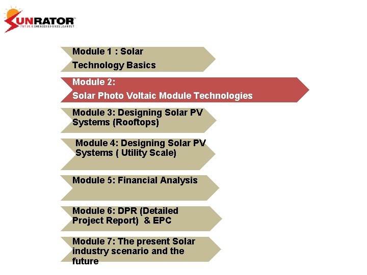
Module 1 : Solar Technology Basics Module 2: Solar Photo Voltaic Module Technologies Module 3: Designing Solar PV Systems (Rooftops) Module 4: Designing Solar PV Systems ( Utility Scale) Module 5: Financial Analysis Module 6: DPR (Detailed Project Report) & EPC Module 7: The present Solar industry scenario and the future

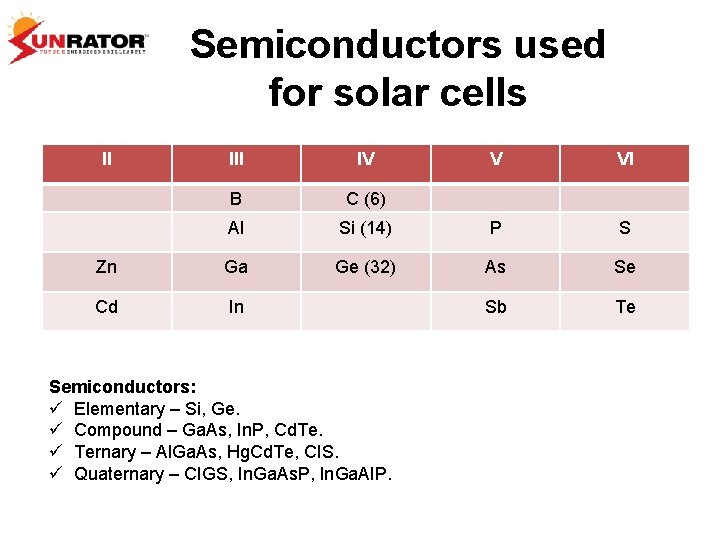
Semiconductors used for solar cells II IV V VI B C (6) Al Si (14) P S Zn Ga Ge (32) As Se Cd In Sb Te Semiconductors: ü Elementary – Si, Ge. ü Compound – Ga. As, In. P, Cd. Te. ü Ternary – Al. Ga. As, Hg. Cd. Te, CIS. ü Quaternary – CIGS, In. Ga. As. P, In. Ga. AIP.

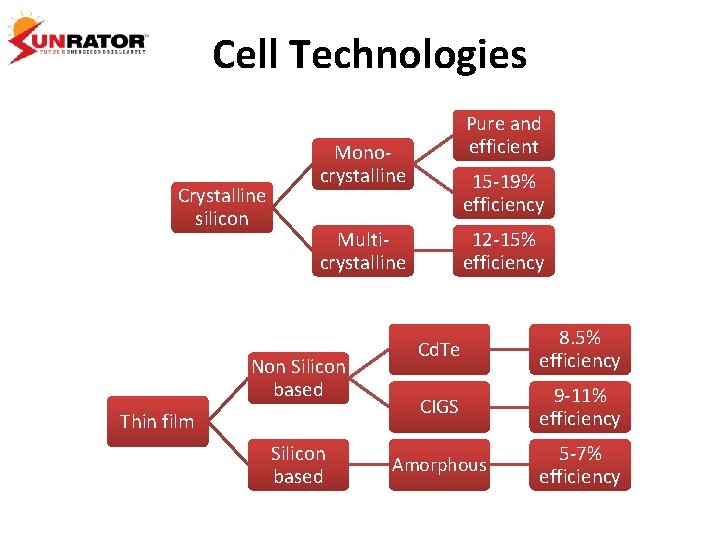
Cell Technologies Crystalline silicon Pure and efficient Monocrystalline 15 -19% efficiency Multicrystalline Non Silicon based Thin film Silicon based 12 -15% efficiency Cd. Te 8. 5% efficiency CIGS 9 -11% efficiency Amorphous 5 -7% efficiency

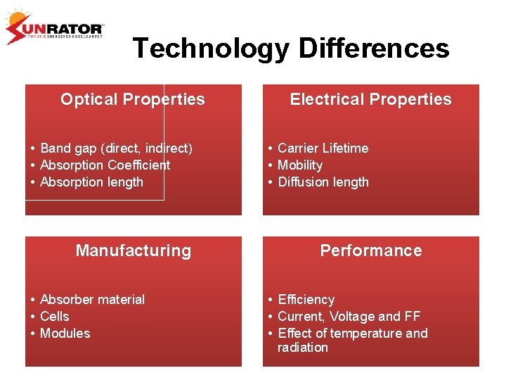
Technology Differences Optical Properties • Band gap (direct, indirect) • Absorption Coefficient • Absorption length Manufacturing • Absorber material • Cells • Modules Electrical Properties • Carrier Lifetime • Mobility • Diffusion length Performance • Efficiency • Current, Voltage and FF • Effect of temperature and radiation

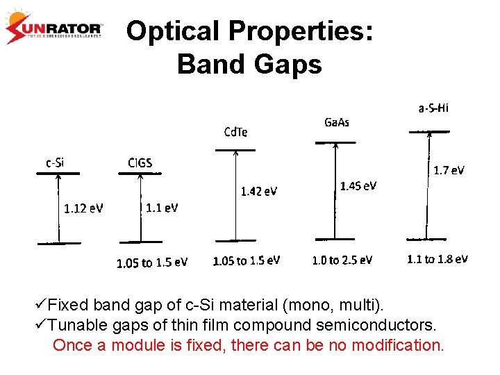
Optical Properties: Band Gaps üFixed band gap of c-Si material (mono, multi). üTunable gaps of thin film compound semiconductors. Once a module is fixed, there can be no modification.

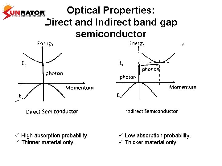
Optical Properties: Direct and Indirect band gap semiconductor ü High absorption probability. ü Thinner material only. ü Low absorption probability. ü Thicker material only.

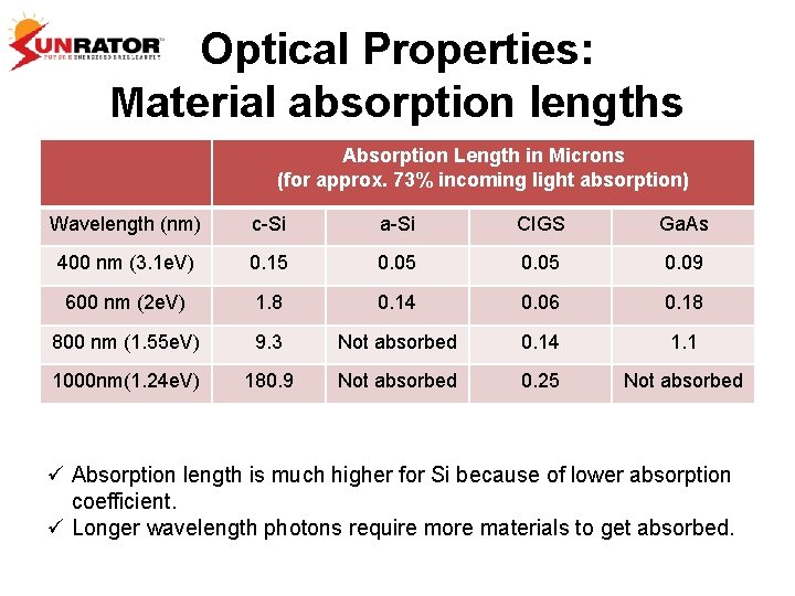
Optical Properties: Material absorption lengths Absorption Length in Microns (for approx. 73% incoming light absorption) Wavelength (nm) c-Si a-Si CIGS Ga. As 400 nm (3. 1 e. V) 0. 15 0. 05 0. 09 600 nm (2 e. V) 1. 8 0. 14 0. 06 0. 18 800 nm (1. 55 e. V) 9. 3 Not absorbed 0. 14 1. 1 1000 nm(1. 24 e. V) 180. 9 Not absorbed 0. 25 Not absorbed ü Absorption length is much higher for Si because of lower absorption coefficient. ü Longer wavelength photons require more materials to get absorbed.

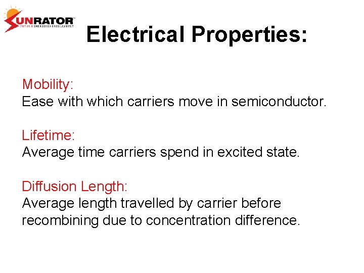
Electrical Properties: Mobility: Ease with which carriers move in semiconductor. Lifetime: Average time carriers spend in excited state. Diffusion Length: Average length travelled by carrier before recombining due to concentration difference.

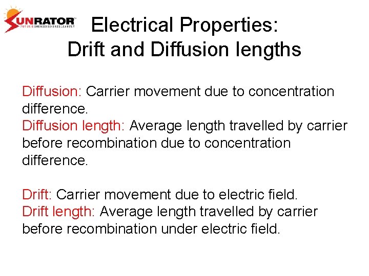
Electrical Properties: Drift and Diffusion lengths Diffusion: Carrier movement due to concentration difference. Diffusion length: Average length travelled by carrier before recombination due to concentration difference. Drift: Carrier movement due to electric field. Drift length: Average length travelled by carrier before recombination under electric field.

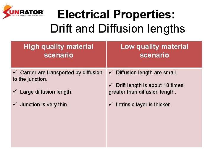
Electrical Properties: Drift and Diffusion lengths High quality material scenario ü Carrier are transported by diffusion to the junction. Low quality material scenario ü Diffusion length are small. ü Large diffusion length. ü Drift length is about 10 times greater than diffusion length. ü Junction is very thin. ü Intrinsic layer is thicker.

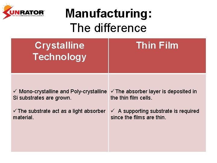
Manufacturing: The difference Crystalline Technology Thin Film ü Mono-crystalline and Poly-crystalline üThe absorber layer is deposited in Si substrates are grown. the thin film cells. üThe substrate act as a light absorber ü A supporting substrate is required material. since the films are thin.

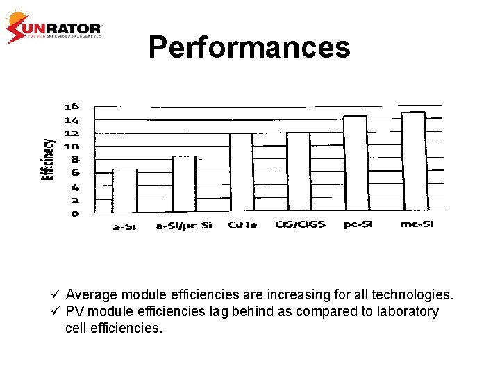
Performances ü Average module efficiencies are increasing for all technologies. ü PV module efficiencies lag behind as compared to laboratory cell efficiencies.

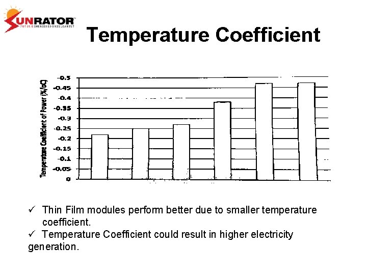
Temperature Coefficient ü Thin Film modules perform better due to smaller temperature coefficient. ü Temperature Coefficient could result in higher electricity generation.

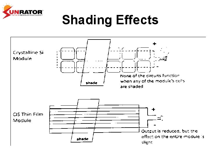
Shading Effects