Module 2 Numbers and Registers The Hexadecimal Number
Module 2: Numbers and Registers
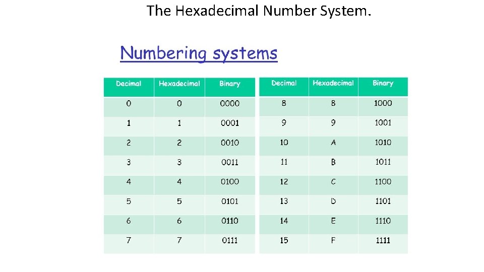
The Hexadecimal Number System.
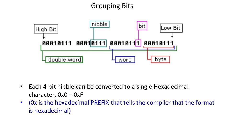
Grouping Bits • Each 4 -bit nibble can be converted to a single Hexadecimal character, 0 x 0 – 0 x. F • (0 x is the hexadecimal PREFIX that tells the compiler that the format is hexadecimal)
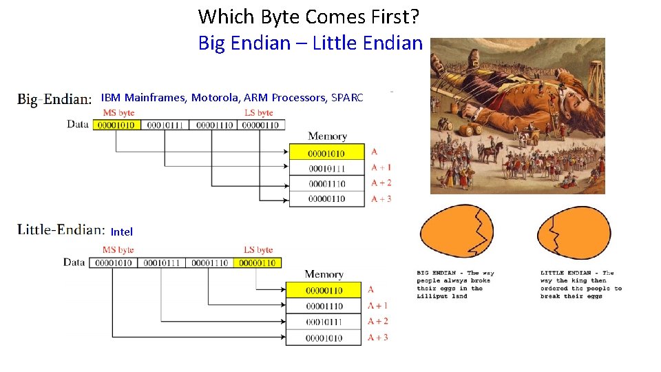
Which Byte Comes First? Big Endian – Little Endian IBM Mainframes, Motorola, ARM Processors, SPARC Intel
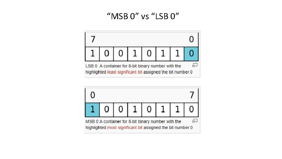
“MSB 0” vs “LSB 0”
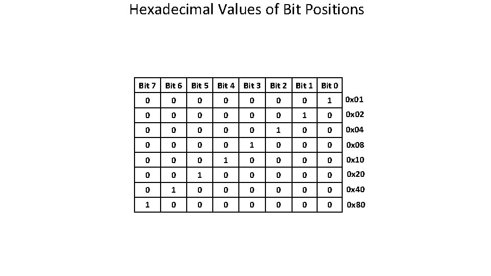
Hexadecimal Values of Bit Positions Bit 7 Bit 6 Bit 5 Bit 4 Bit 3 Bit 2 Bit 1 Bit 0 0 0 0 1 0 x 01 0 0 0 1 0 0 x 02 0 0 0 1 0 0 0 x 04 0 0 1 0 0 x 08 0 0 0 1 0 0 0 x 10 0 0 1 0 0 0 x 20 0 1 0 0 0 0 x 40 1 0 0 0 0 x 80
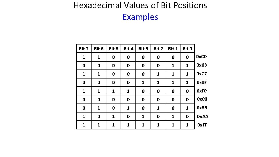
Hexadecimal Values of Bit Positions Examples Bit 7 Bit 6 Bit 5 Bit 4 Bit 3 Bit 2 Bit 1 Bit 0 1 1 0 0 0 0 x. C 0 0 0 0 1 1 0 x 03 1 1 0 0 0 1 1 1 0 x. C 7 0 0 1 1 0 x 0 F 1 1 0 0 0 x. F 0 0 0 0 0 x 00 0 1 0 1 0 x 55 1 0 1 0 0 x. AA 1 1 1 1 0 x. FF
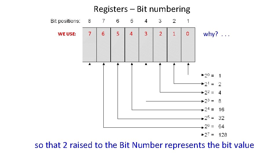
Registers – Bit numbering WE USE: 7 6 5 4 3 2 1 0 why? . . . so that 2 raised to the Bit Number represents the bit value
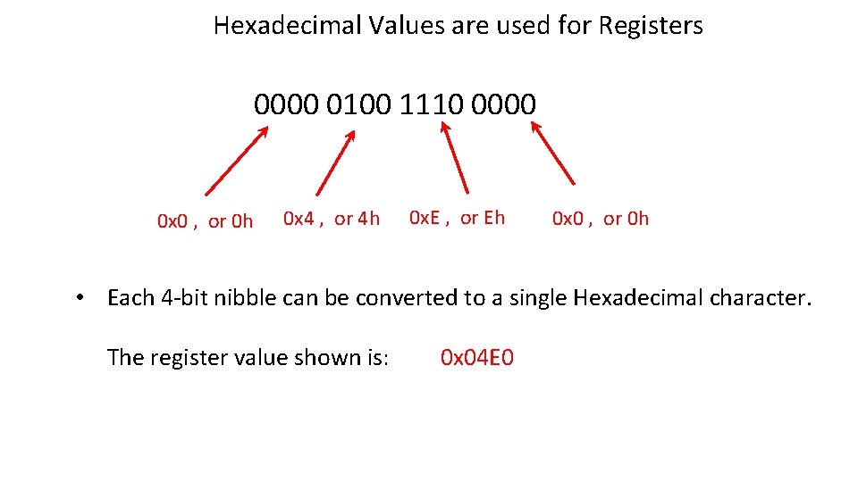
Hexadecimal Values are used for Registers 0000 0100 1110 0000 0 x 0 , or 0 h 0 x 4 , or 4 h 0 x. E , or Eh 0 x 0 , or 0 h • Each 4 -bit nibble can be converted to a single Hexadecimal character. The register value shown is: 0 x 04 E 0
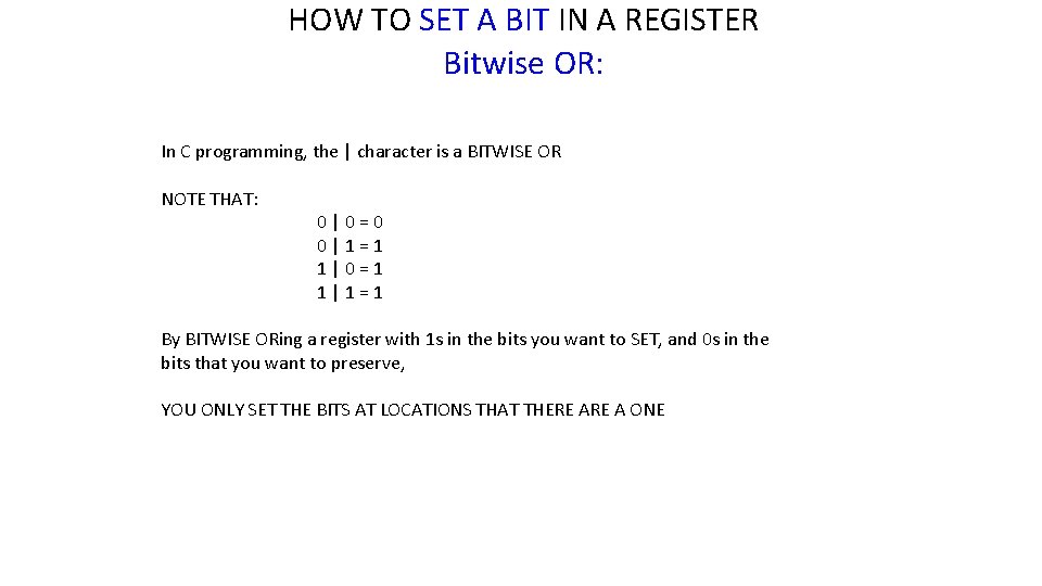
HOW TO SET A BIT IN A REGISTER Bitwise OR: In C programming, the | character is a BITWISE OR NOTE THAT: 0|0=0 0|1=1 1|0=1 1|1=1 By BITWISE ORing a register with 1 s in the bits you want to SET, and 0 s in the bits that you want to preserve, YOU ONLY SET THE BITS AT LOCATIONS THAT THERE A ONE
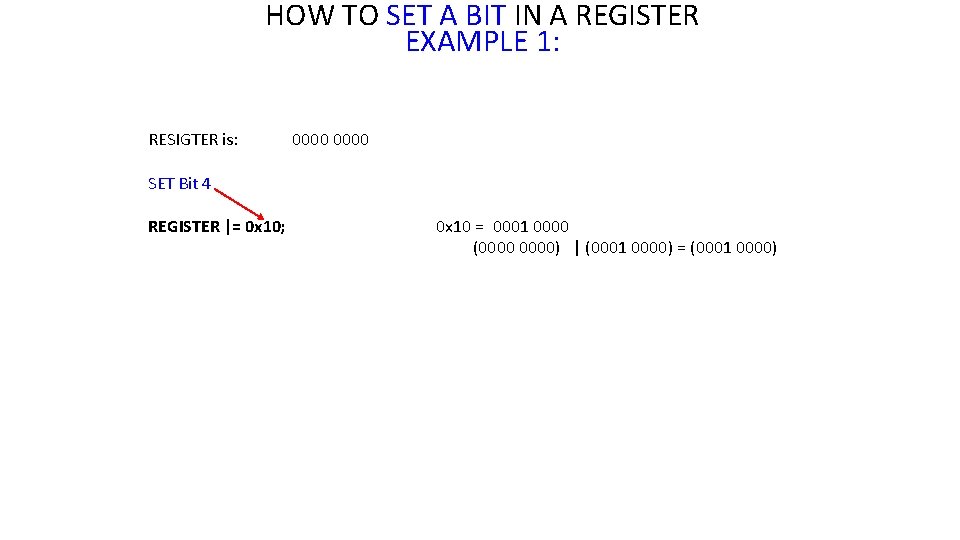
HOW TO SET A BIT IN A REGISTER EXAMPLE 1: RESIGTER is: 0000 SET Bit 4 REGISTER |= 0 x 10; 0 x 10 = 0001 0000 (0000) | (0001 0000) = (0001 0000)
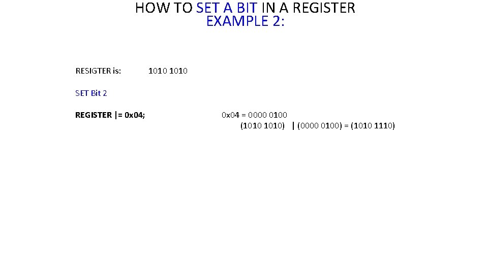
HOW TO SET A BIT IN A REGISTER EXAMPLE 2: RESIGTER is: 1010 SET Bit 2 REGISTER |= 0 x 04; 0 x 04 = 0000 0100 (1010) | (0000 0100) = (1010 1110)
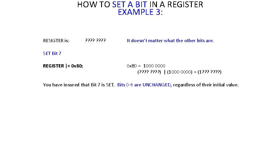
HOW TO SET A BIT IN A REGISTER EXAMPLE 3: RESIGTER is: ? ? ? ? It doesn’t matter what the other bits are. SET Bit 7 REGISTER |= 0 x 80; 0 x 80 = 1000 0000 (? ? ? ? ) | (1000 0000) = (1? ? ? ? ) You have insured that Bit 7 is SET. Bits 0 -6 are UNCHANGED, regardless of their initial value.
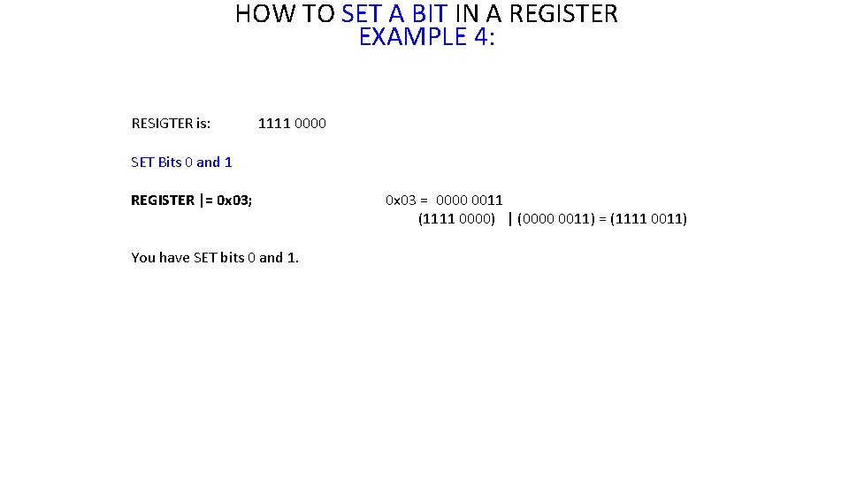
HOW TO SET A BIT IN A REGISTER EXAMPLE 4: RESIGTER is: 1111 0000 SET Bits 0 and 1 REGISTER |= 0 x 03; You have SET bits 0 and 1. 0 x 03 = 0000 0011 (1111 0000) | (0000 0011) = (1111 0011)
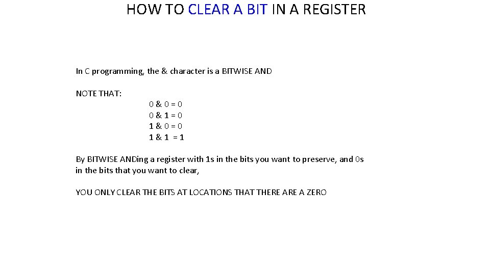
HOW TO CLEAR A BIT IN A REGISTER In C programming, the & character is a BITWISE AND NOTE THAT: 0&0=0 0&1=0 1&0=0 1&1 =1 By BITWISE ANDing a register with 1 s in the bits you want to preserve, and 0 s in the bits that you want to clear, YOU ONLY CLEAR THE BITS AT LOCATIONS THAT THERE A ZERO
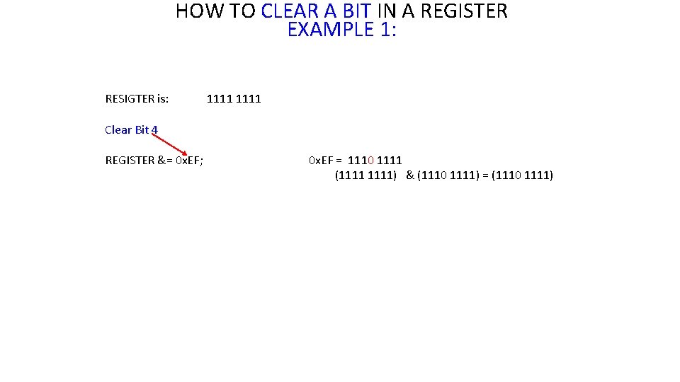
HOW TO CLEAR A BIT IN A REGISTER EXAMPLE 1: RESIGTER is: 1111 Clear Bit 4 REGISTER &= 0 x. EF; 0 x. EF = 1110 1111 (1111) & (1110 1111) = (1110 1111)

HOW TO CLEAR A BIT IN A REGISTER EXAMPLE 2: RESIGTER is: Clear Bit 3 REGISTER &= 0 x. F 7; 1010 Bit 3 0 x. F 7 = 1111 0111 (1010) & (1111 0111) = (1010 0010)
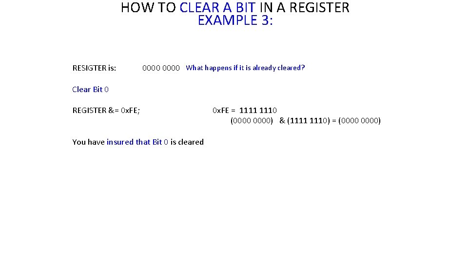
HOW TO CLEAR A BIT IN A REGISTER EXAMPLE 3: RESIGTER is: 0000 What happens if it is already cleared? Clear Bit 0 REGISTER &= 0 x. FE; You have insured that Bit 0 is cleared 0 x. FE = 1111 1110 (0000) & (1111 1110) = (0000)
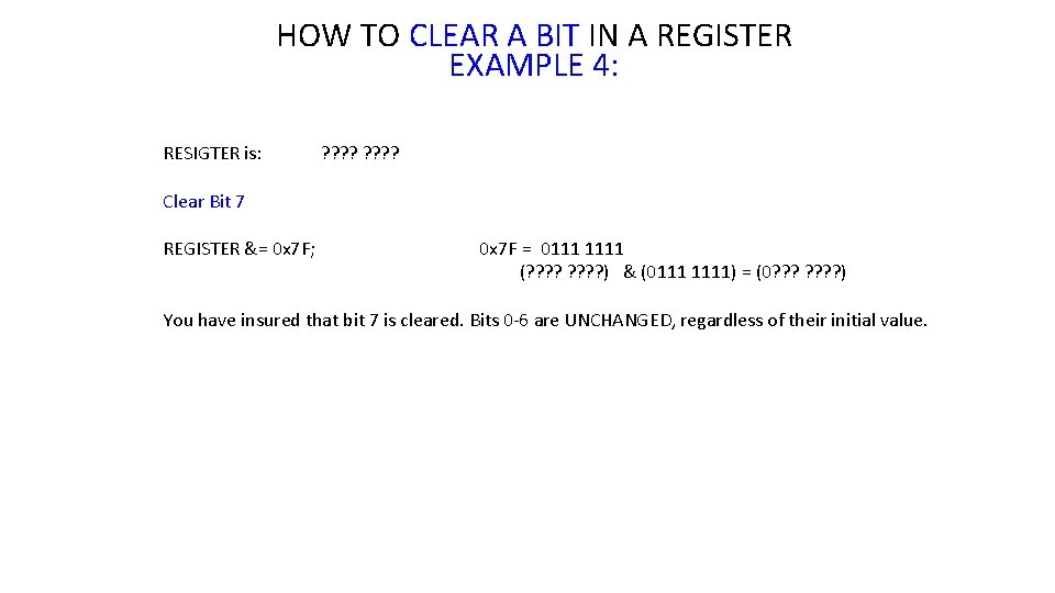
HOW TO CLEAR A BIT IN A REGISTER EXAMPLE 4: RESIGTER is: ? ? ? ? Clear Bit 7 REGISTER &= 0 x 7 F; 0 x 7 F = 0111 1111 (? ? ? ? ) & (0111 1111) = (0? ? ? ? ) You have insured that bit 7 is cleared. Bits 0 -6 are UNCHANGED, regardless of their initial value.
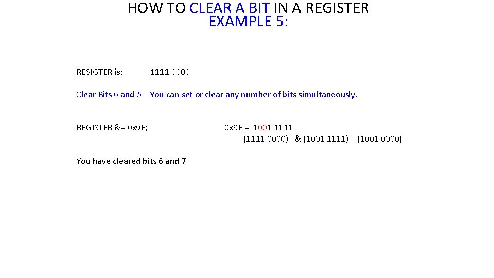
HOW TO CLEAR A BIT IN A REGISTER EXAMPLE 5: RESIGTER is: 1111 0000 Clear Bits 6 and 5 You can set or clear any number of bits simultaneously. REGISTER &= 0 x 9 F; You have cleared bits 6 and 7 0 x 9 F = 1001 1111 (1111 0000) & (1001 1111) = (1001 0000)
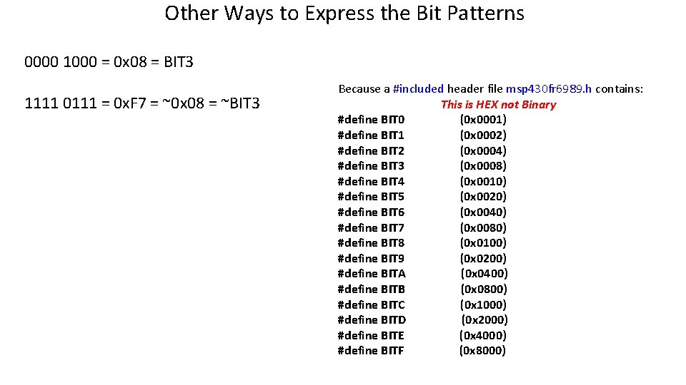
Other Ways to Express the Bit Patterns 0000 1000 = 0 x 08 = BIT 3 1111 0111 = 0 x. F 7 = ~0 x 08 = ~BIT 3 Because a #included header file msp 430 fr 6989. h contains: This is HEX not Binary #define BIT 0 (0 x 0001) #define BIT 1 (0 x 0002) #define BIT 2 (0 x 0004) #define BIT 3 (0 x 0008) #define BIT 4 (0 x 0010) #define BIT 5 (0 x 0020) #define BIT 6 (0 x 0040) #define BIT 7 (0 x 0080) #define BIT 8 (0 x 0100) #define BIT 9 (0 x 0200) #define BITA (0 x 0400) #define BITB (0 x 0800) #define BITC (0 x 1000) #define BITD (0 x 2000) #define BITE (0 x 4000) #define BITF (0 x 8000)
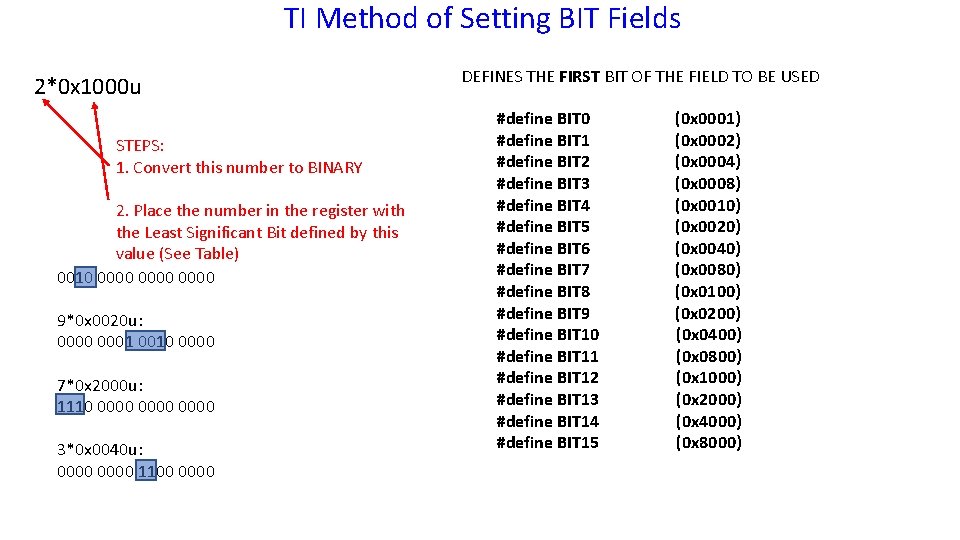
TI Method of Setting BIT Fields 2*0 x 1000 u STEPS: 1. Convert this number to BINARY 2. Place the number in the register with the Least Significant Bit defined by this value (See Table) 0010 0000 9*0 x 0020 u: 0000 0001 0010 0000 7*0 x 2000 u: 1110 0000 3*0 x 0040 u: 0000 1100 0000 DEFINES THE FIRST BIT OF THE FIELD TO BE USED #define BIT 0 #define BIT 1 #define BIT 2 #define BIT 3 #define BIT 4 #define BIT 5 #define BIT 6 #define BIT 7 #define BIT 8 #define BIT 9 #define BIT 10 #define BIT 11 #define BIT 12 #define BIT 13 #define BIT 14 #define BIT 15 (0 x 0001) (0 x 0002) (0 x 0004) (0 x 0008) (0 x 0010) (0 x 0020) (0 x 0040) (0 x 0080) (0 x 0100) (0 x 0200) (0 x 0400) (0 x 0800) (0 x 1000) (0 x 2000) (0 x 4000) (0 x 8000)
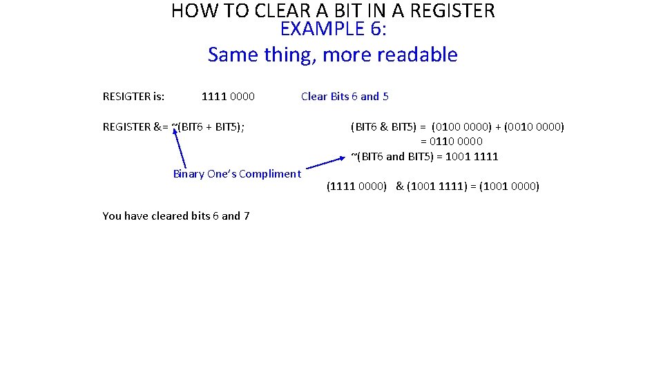
HOW TO CLEAR A BIT IN A REGISTER EXAMPLE 6: Same thing, more readable RESIGTER is: 1111 0000 REGISTER &= ~(BIT 6 + BIT 5); Binary One’s Compliment You have cleared bits 6 and 7 Clear Bits 6 and 5 (BIT 6 & BIT 5) = (0100 0000) + (0010 0000) = 0110 0000 ~(BIT 6 and BIT 5) = 1001 1111 (1111 0000) & (1001 1111) = (1001 0000)
Module 3: The MSP 430 FR 6989 Microcontroller
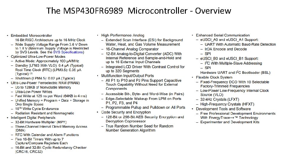
The MSP 430 FR 6989 Microcontroller - Overview
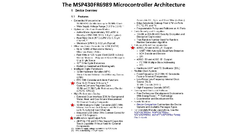
The MSP 430 FR 6989 Microcontroller Architecture
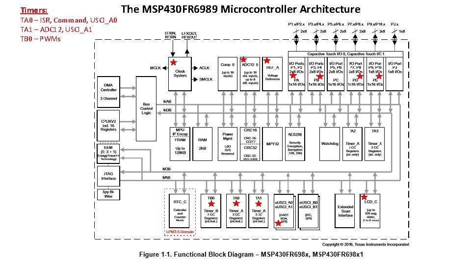
Timers: TA 0 – ISR, Command, USCI_A 0 TA 1 – ADC 12, USCI_A 1 TB 0 – PWMs The MSP 430 FR 6989 Microcontroller Architecture
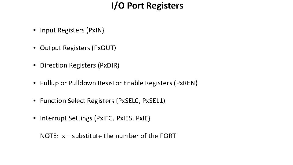
I/O Port Registers • Input Registers (Px. IN) • Output Registers (Px. OUT) • Direction Registers (Px. DIR) • Pullup or Pulldown Resistor Enable Registers (Px. REN) • Function Select Registers (Px. SEL 0, Px. SEL 1) • Interrupt Settings (Px. IFG, Px. IES, Px. IE) NOTE: x – substitute the number of the PORT
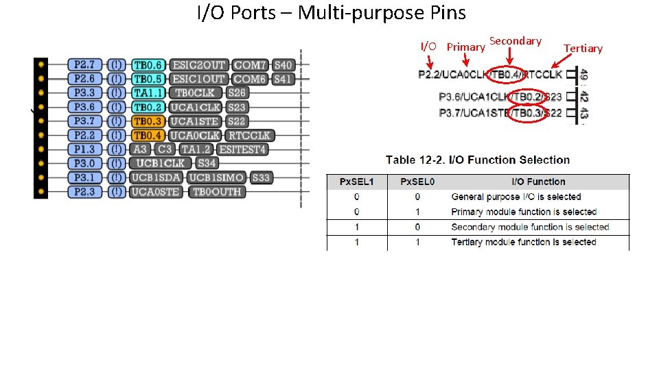
I/O Ports – Multi-purpose Pins I/O Primary Secondary Tertiary
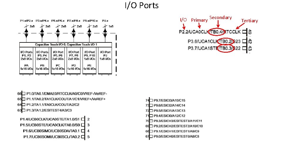
I/O Ports I/O Primary Secondary Tertiary
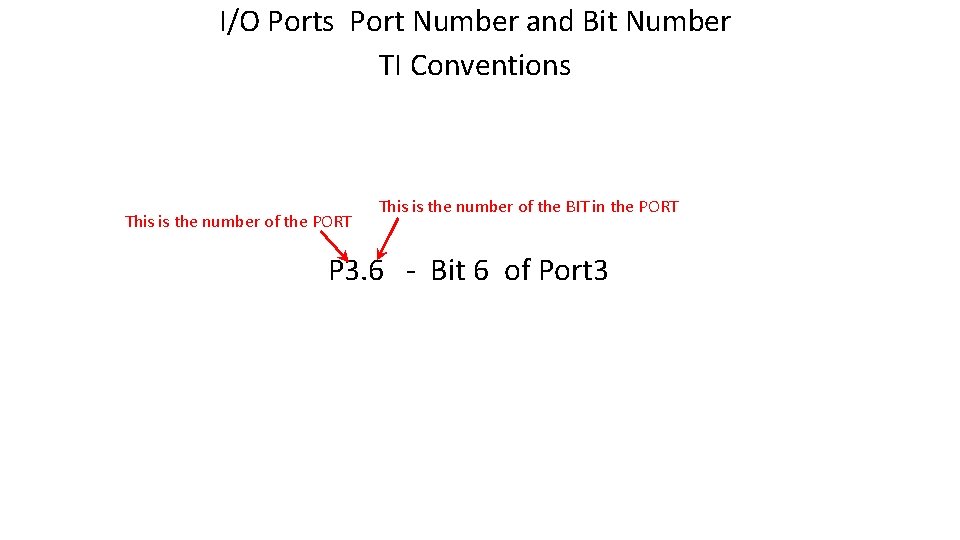
I/O Ports Port Number and Bit Number TI Conventions This is the number of the PORT This is the number of the BIT in the PORT P 3. 6 - Bit 6 of Port 3
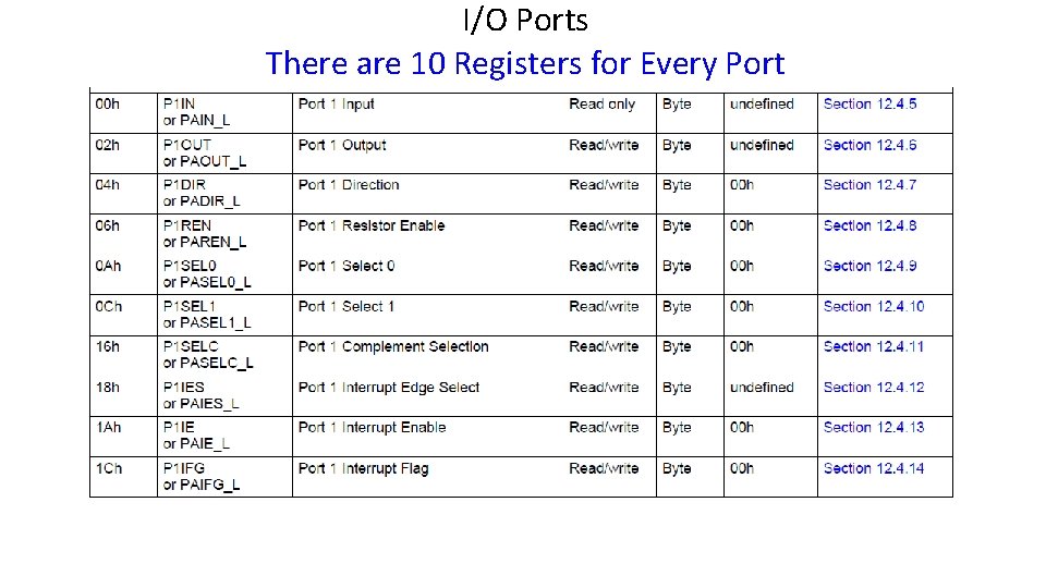
I/O Ports There are 10 Registers for Every Port

I/O Ports
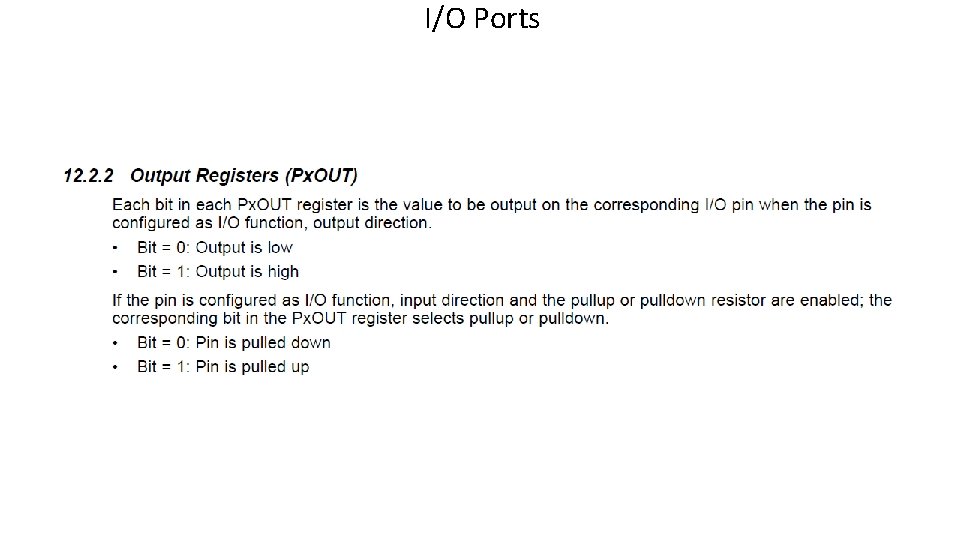
I/O Ports

I/O Ports

I/O Ports
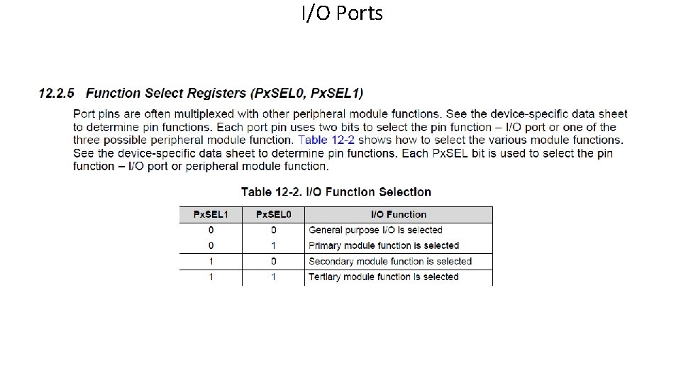
I/O Ports
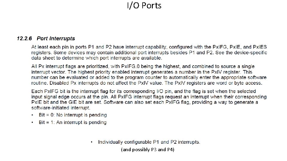
I/O Ports (and possibly P 3 and P 4)
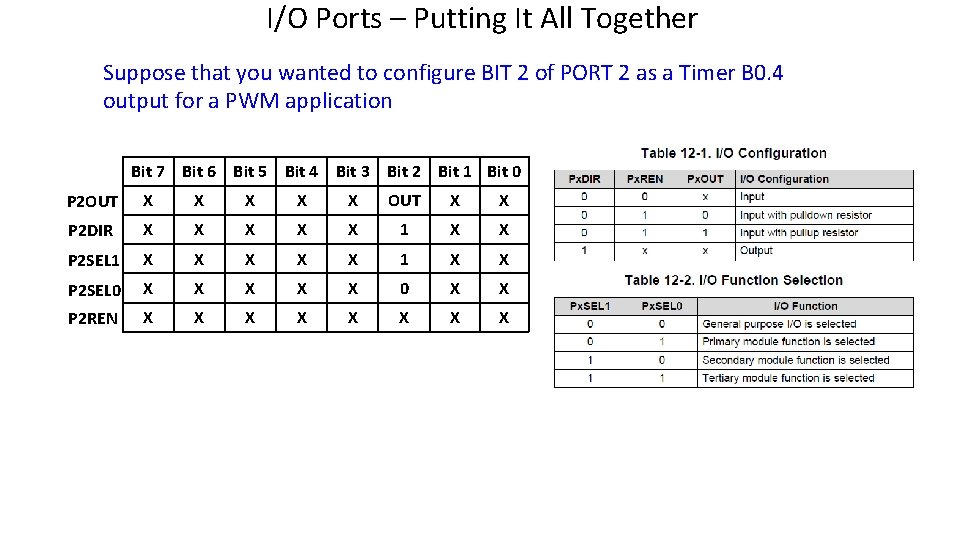
I/O Ports – Putting It All Together Suppose that you wanted to configure BIT 2 of PORT 2 as a Timer B 0. 4 output for a PWM application Bit 7 Bit 6 Bit 5 Bit 4 Bit 3 Bit 2 Bit 1 Bit 0 P 2 OUT X X X OUT X X P 2 DIR X X X 1 X X P 2 SEL 1 X X X 1 X X P 2 SEL 0 X X X 0 X X P 2 REN X X X X
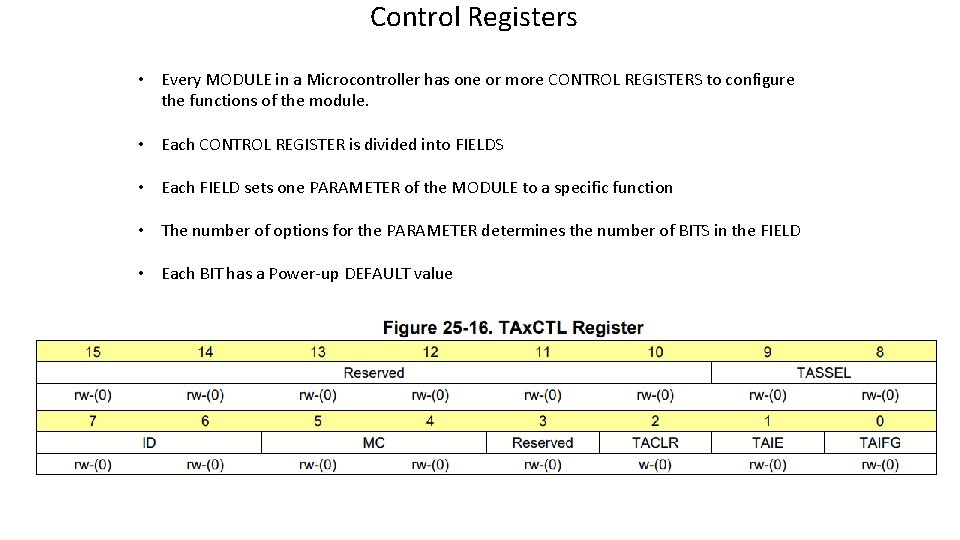
Control Registers • Every MODULE in a Microcontroller has one or more CONTROL REGISTERS to configure the functions of the module. • Each CONTROL REGISTER is divided into FIELDS • Each FIELD sets one PARAMETER of the MODULE to a specific function • The number of options for the PARAMETER determines the number of BITS in the FIELD • Each BIT has a Power-up DEFAULT value
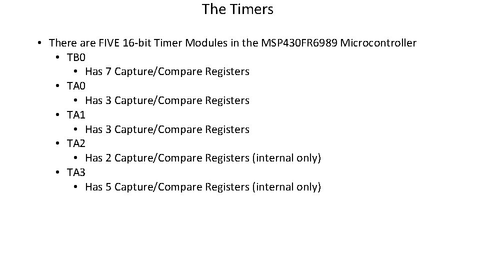
The Timers • There are FIVE 16 -bit Timer Modules in the MSP 430 FR 6989 Microcontroller • TB 0 • Has 7 Capture/Compare Registers • TA 0 • Has 3 Capture/Compare Registers • TA 1 • Has 3 Capture/Compare Registers • TA 2 • Has 2 Capture/Compare Registers (internal only) • TA 3 • Has 5 Capture/Compare Registers (internal only)
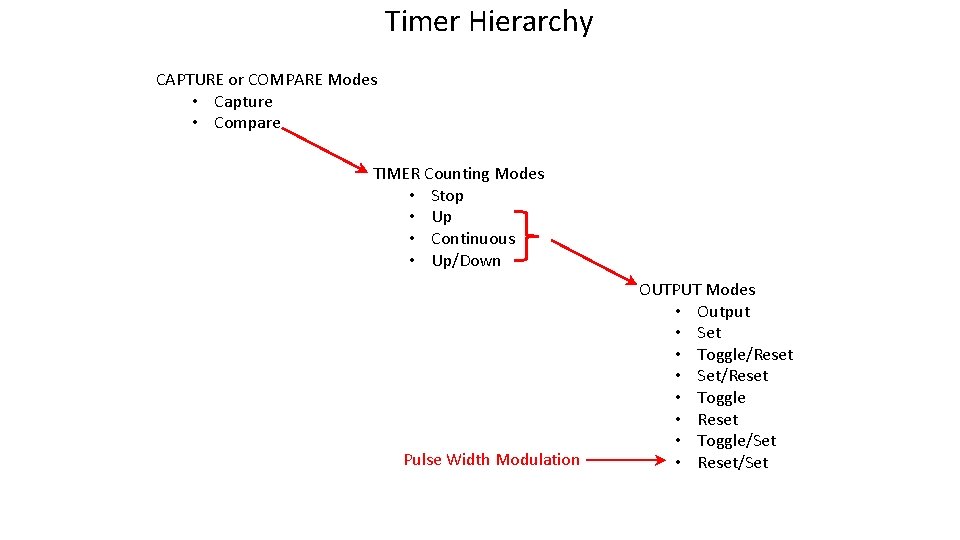
Timer Hierarchy CAPTURE or COMPARE Modes • Capture • Compare TIMER Counting Modes • Stop • Up • Continuous • Up/Down Pulse Width Modulation OUTPUT Modes • Output • Set • Toggle/Reset • Set/Reset • Toggle • Reset • Toggle/Set • Reset/Set
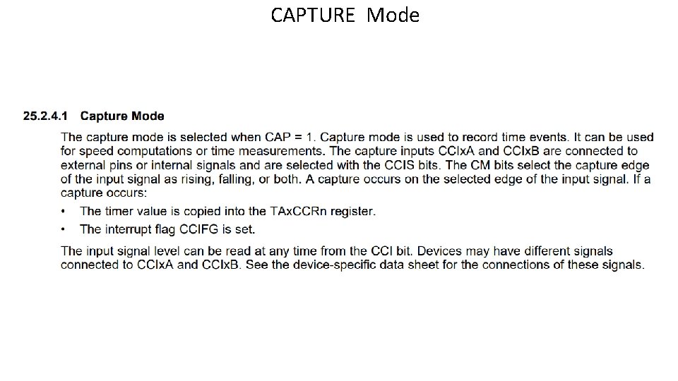
CAPTURE Mode
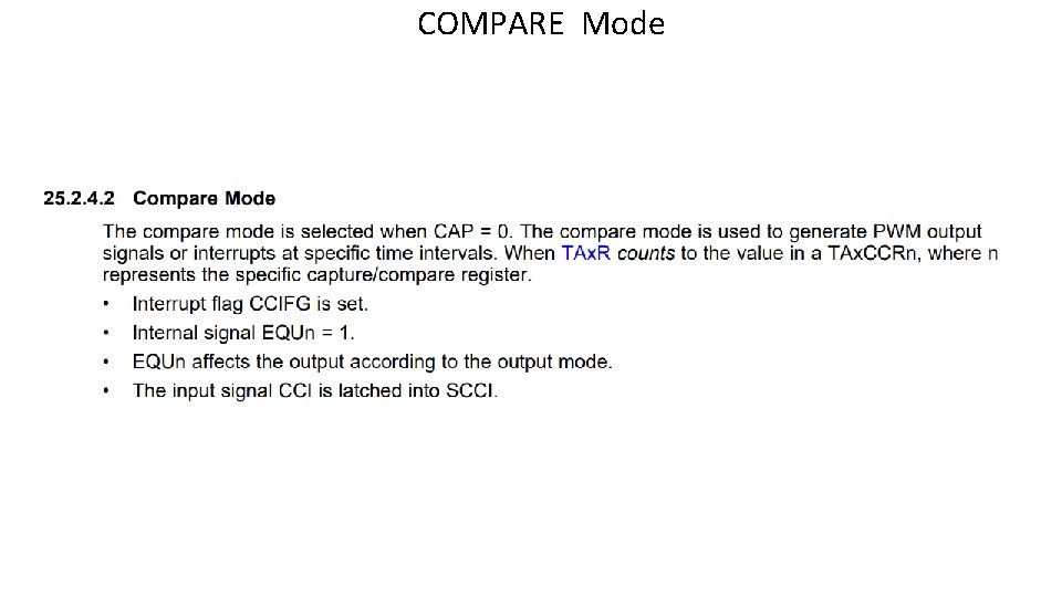
COMPARE Mode

TIMER Modes • There FOUR Timer MODES: This describes what the COUNTER is doing (TAx. R or TB 0 R) • STOP Mode • UP Mode • Continuous Mode • UP/DOWN Mode

UP Mode
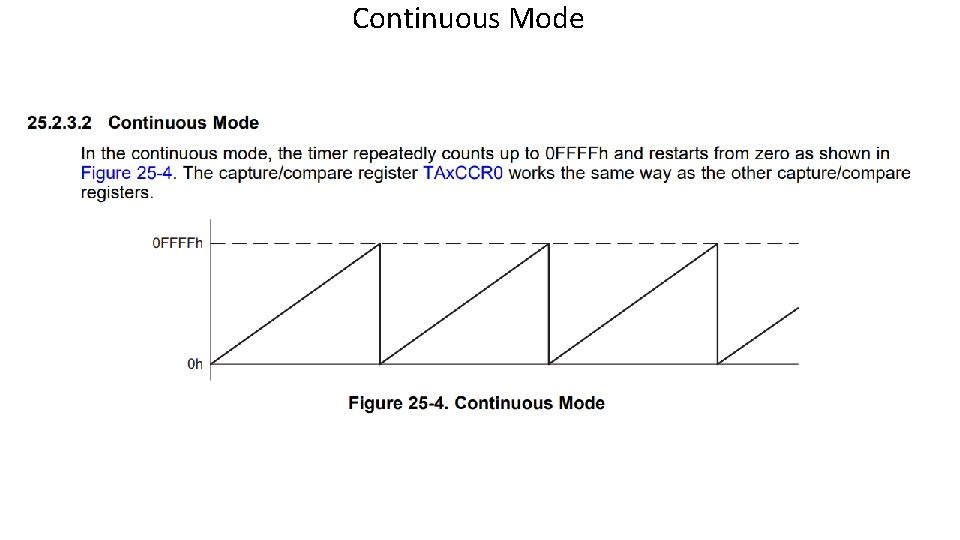
Continuous Mode

Up/Down Mode

UP Mode

OUTPUT Modes • There EIGHT OUTPUT MODES: • This describes what the OUTPUT SIGNAL is doing (OUT 1 – OUT 6 on TBO e. g. ) • Compare Registers are used to SET or CLEAR the OUTPUT signal
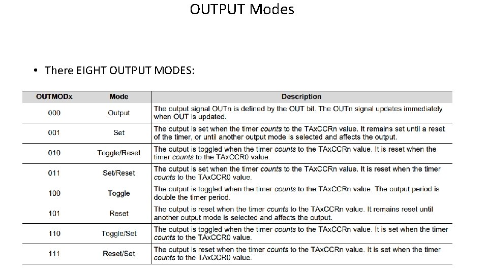
OUTPUT Modes • There EIGHT OUTPUT MODES:
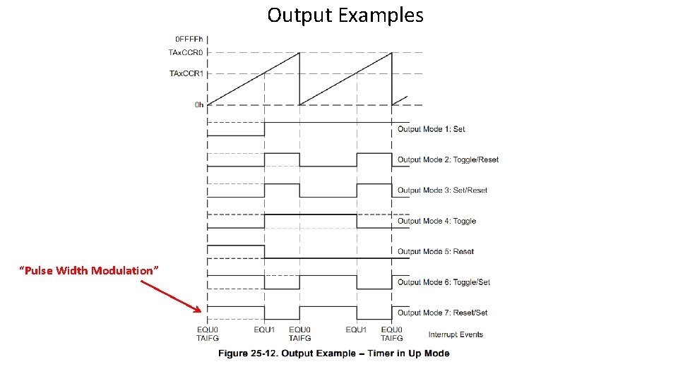
Output Examples “Pulse Width Modulation”
Interrupt Service Routines • Require a #pragma vector= NAME_OF_VECTOR • There is USUALLY an unused_interrupt file with all of the #pragmas for all possible interrupts. The vector you wish to use must be commented out in the unused_interrupt source file. • ISR must be preceded by the reserved for implementation name of : __interrupt
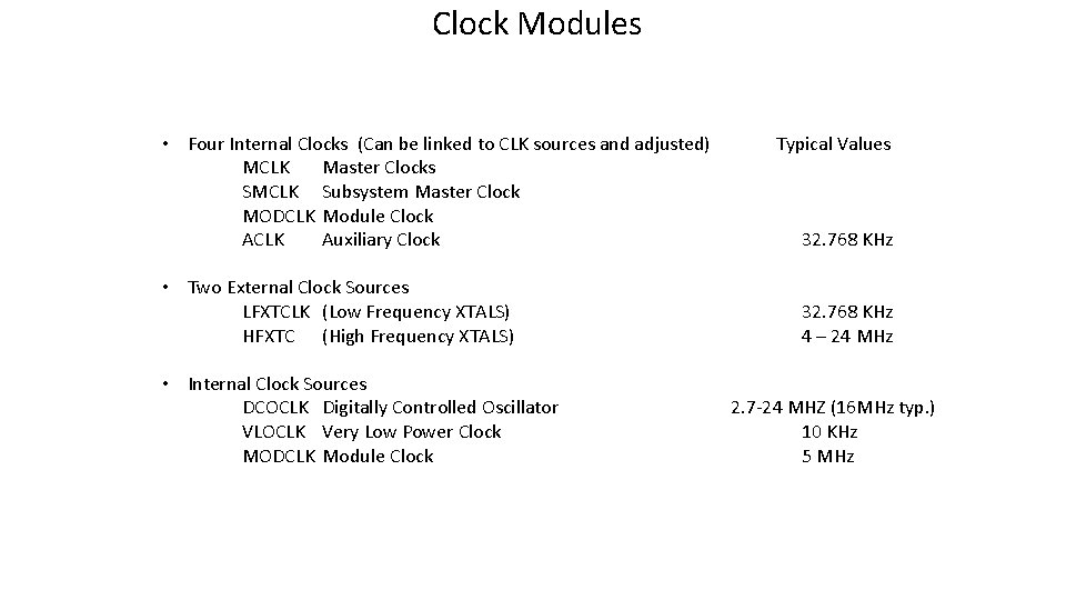
Clock Modules • Four Internal Clocks (Can be linked to CLK sources and adjusted) MCLK Master Clocks SMCLK Subsystem Master Clock MODCLK Module Clock ACLK Auxiliary Clock • Two External Clock Sources LFXTCLK (Low Frequency XTALS) HFXTC (High Frequency XTALS) • Internal Clock Sources DCOCLK Digitally Controlled Oscillator VLOCLK Very Low Power Clock MODCLK Module Clock Typical Values 32. 768 KHz 4 – 24 MHz 2. 7 -24 MHZ (16 MHz typ. ) 10 KHz 5 MHz
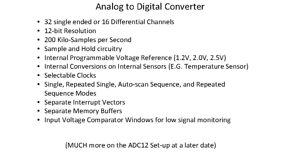
Analog to Digital Converter 32 single ended or 16 Differential Channels 12 -bit Resolution 200 Kilo-Samples per Second Sample and Hold circuitry Internal Programmable Voltage Reference (1. 2 V, 2. 0 V, 2. 5 V) Internal Conversions on Internal Sensors (E. G. Temperature Sensor) Selectable Clocks Single, Repeated Single, Auto-scan Sequence, and Repeated Sequence Modes • Separate Interrupt Vectors • Separate Memory Buffers • Input Voltage Comparator Windows for low signal monitoring • • (MUCH more on the ADC 12 Set-up at a later date)

NEXT WEEK: Lab 1/ Quiz 1: Code Composer, Project Creation, GPIO, and Interrupts

Lab Instructions (General): 1. Watch the Video for the Lab at u. osu. edu/ece 3567 labs BEFORE coming to the Lab session.

Lab Instructions (General): 2. Take the Quiz (in class, closed note) to verify that you have watched and understood the prelab video.

Lab Instructions (General): 3. Perform the Lab, referring to the video and/or instructions slides
Lab Instructions (General): • For Lab 1 you will have detailed instructions and only 1 lab session to complete the lab. • DO NOT simply copy the slides. You must understand what each step does, or you will not be able to troubleshoot your project. • All other labs will require you to write your own code, and you are given 2 weeks to complete the Lab.
Lab Instructions (General): 4. Demonstrate the working Lab project to the Lab Staff to earn the Lab CHECKPOINTS The list of lab checkpoints will be included in the pre-lab material NOTE: The best approach is to get one checkpoint at a time to verify that your design is functioning at that point, prior to moving to the next step in the lab.

Lab Instructions (General): 5. VERIFY that you received your Checkpoints in writing by signing off on the Checkpoint Sheet before leaving the laboratory.
- Slides: 62